Blog
Industry insights, engineering guides, and expert analysis for PCB professionals
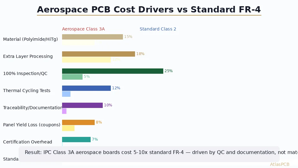
Aerospace PCB Pricing: Why IPC Class 3A Boards Cost 5-10x More and How to Optimize
Detailed cost breakdown of aerospace-grade PCB fabrication to IPC-6012 Class 3/3A and AS9100 requirements. Identifies the actual cost drivers — inspection, documentation, and yield loss from coupon allocation — and provides strategies to reduce spend by 20-35% without compromising certification compliance.
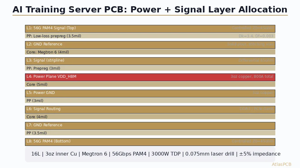
PCB Requirements for AI Training Server Blades: 56G PAM4 Channels and 3000W Power Delivery
Complete PCB specification guide for AI/ML training server blades carrying 56G PAM4 SerDes, HBM3 memory interfaces, and 3000W+ power delivery networks. Covers material selection, stackup architecture, power plane design, and thermal via strategies specific to GPU/TPU accelerator cards.
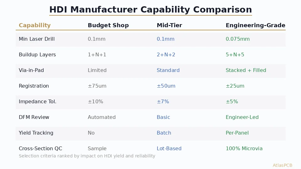
HDI PCB Manufacturer Selection: Budget Board House vs Engineering-Grade Fabricator
How to evaluate HDI PCB manufacturers beyond price per panel. Compares budget shops offering basic 1+N+1 buildup against engineering-grade fabricators with stacked microvias, via-in-pad, and per-panel yield tracking — with decision criteria for prototype vs production.
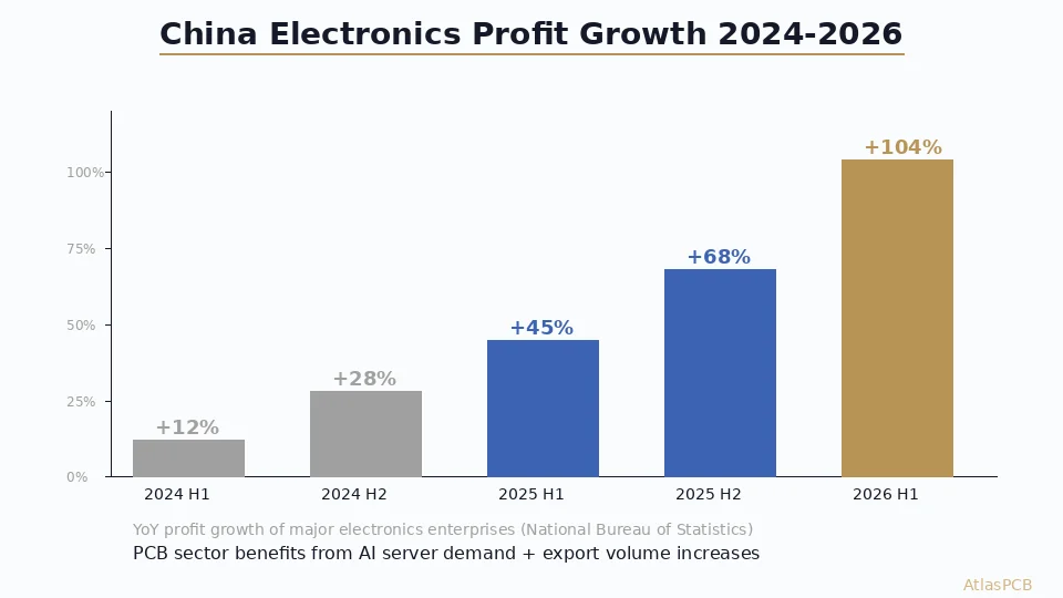
China Electronics Manufacturing Profits Surge 104% in H1 2026: Impact on PCB Pricing and Capacity
China's major electronics manufacturers report a 103.9% year-over-year profit surge in early 2026, driven by AI server demand and export growth. Analysis of how this boom affects PCB supply chain pricing, lead times, and capacity allocation for international customers.
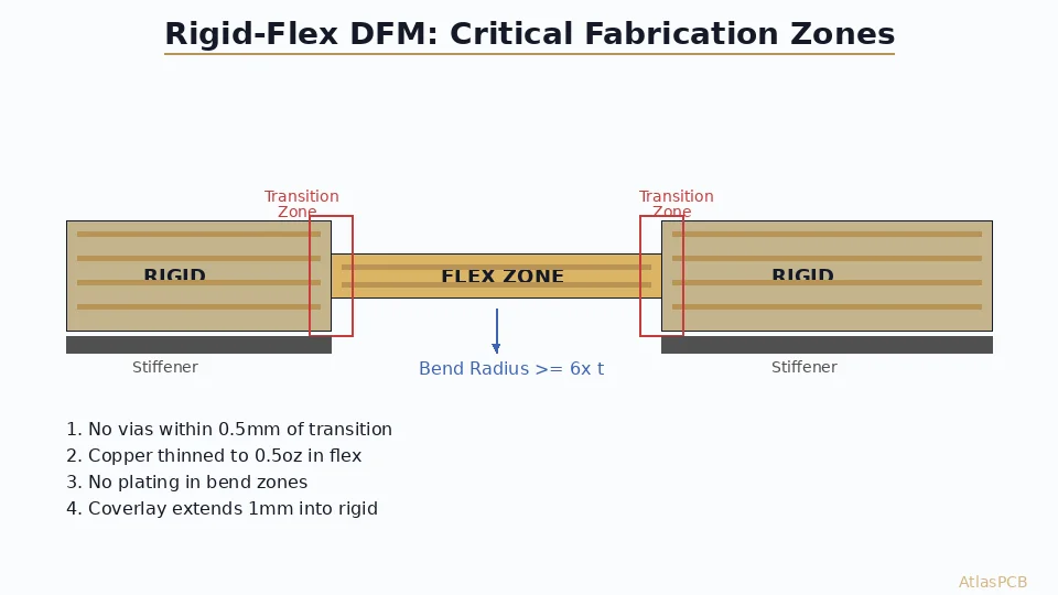
Rigid-Flex PCB DFM: 7 Fabrication Constraints Your EDA Tool Won't Catch
Critical rigid-flex DFM rules that go beyond standard design rule checks. Covers transition zone violations, copper stress relief, coverlay overlap requirements, and bend zone plating — the issues that cause yield loss at the fabricator even when your design passes DRC.
EV Battery Management PCB: Rigid-Flex Design and Manufacturing Requirements for 800V BMS
Engineering guide for PCB design and manufacturing of 800V EV battery management systems. Covers rigid-flex construction for cell-to-module connections, creepage distance requirements at high voltage, thermal management of balancing circuits, and IPC/automotive qualification requirements for BMS PCBs.
Multilayer PCB Cost in 2026: Complete Pricing Analysis from 4-Layer to 20-Layer with Volume Scaling
Updated 2026 pricing analysis for multilayer PCBs covering 4 to 20+ layers. Includes real per-board cost ranges at prototype and production volumes, identifies the specific cost drivers at each layer count threshold, and provides actionable optimization strategies that reduce total fabrication spend by 15-35%.
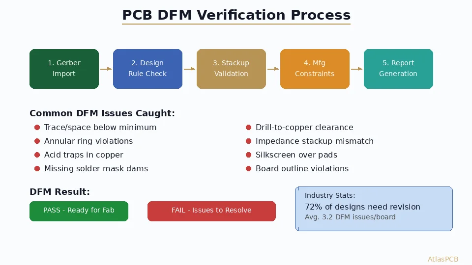
PCB DFM Check Before Ordering: 12-Point Verification That Prevents Costly Respins
A practical DFM verification checklist for engineers about to place a PCB fabrication order. Covers the 12 most common manufacturability issues that cause order rejection, yield loss, or design respins — with specific thresholds and how to fix each one.
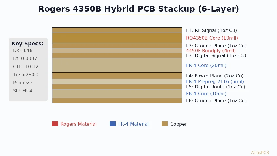
Rogers 4350B Stackup Design for 77 GHz Automotive Radar: 6-Layer Hybrid Configuration Guide
Complete stackup design guide for 77 GHz automotive radar PCBs using Rogers 4350B in a hybrid FR-4 configuration. Covers layer assignment, prepreg selection, impedance targets, and manufacturing constraints specific to ADAS radar modules.
China RF PCB Manufacturer vs Domestic (US/EU): Lead Time, Cost, and Quality Reality Check for 2026
An objective comparison of sourcing RF PCBs from China versus domestic (US/EU) manufacturers. Covers actual lead times, cost differentials at different volumes, quality certifications, and the specific scenarios where each option delivers better value for RF and high-frequency designs.
HDI PCB Manufacturer Pricing: 1+N+1 vs 2+N+2 Cost Breakdown and Build-Up Selection Guide
Detailed cost analysis comparing 1+N+1 and 2+N+2 HDI build-ups. Understand why each additional microvia layer adds 35-50% to PCB cost, which design choices drive the premium, and when 2+N+2 delivers enough routing density to avoid adding expensive standard layers.
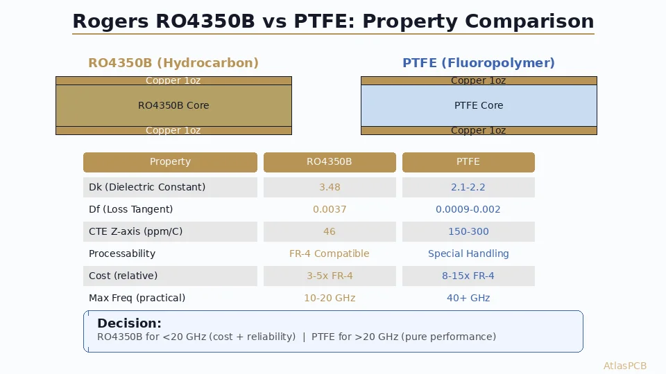
Rogers 4350B vs PTFE for 5G Antenna Array Feed Networks: Material Selection at 28 GHz and 39 GHz
Choosing between Rogers RO4350B and PTFE-based laminates for 5G mmWave antenna array feed networks. Covers insertion loss comparison at 28 GHz and 39 GHz, manufacturing process compatibility, cost analysis, and hybrid stackup strategies that balance RF performance with fabrication yield.
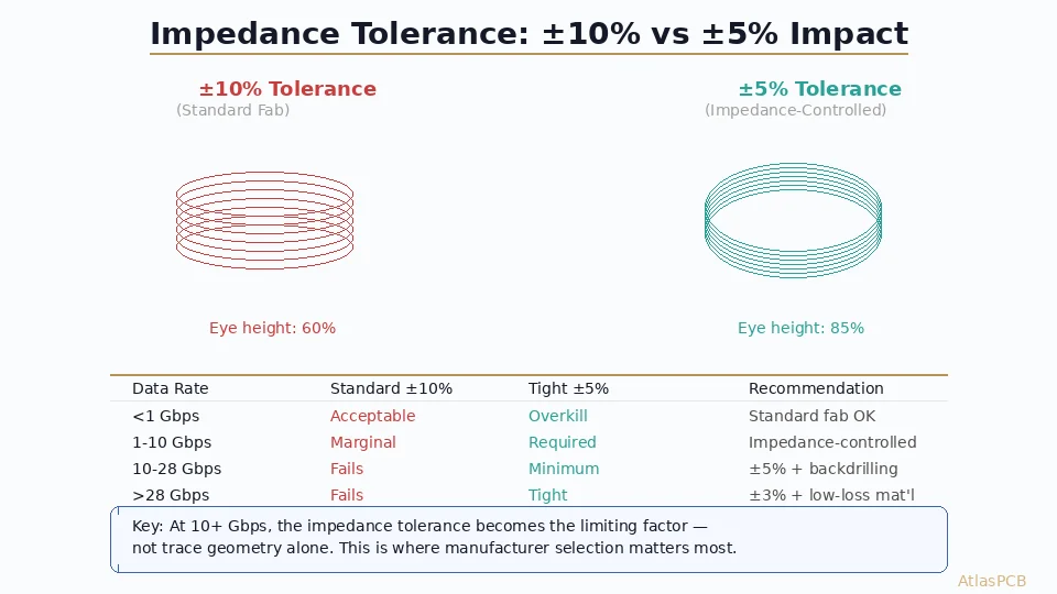
Impedance Controlled PCB: ±10% Standard vs ±5% Tight Tolerance — When It Actually Matters
Not every board needs tight impedance control. This guide explains exactly where the ±10% vs ±5% tolerance boundary lies, what manufacturing processes create the difference, and how to specify impedance requirements without over-engineering or under-specifying your design.
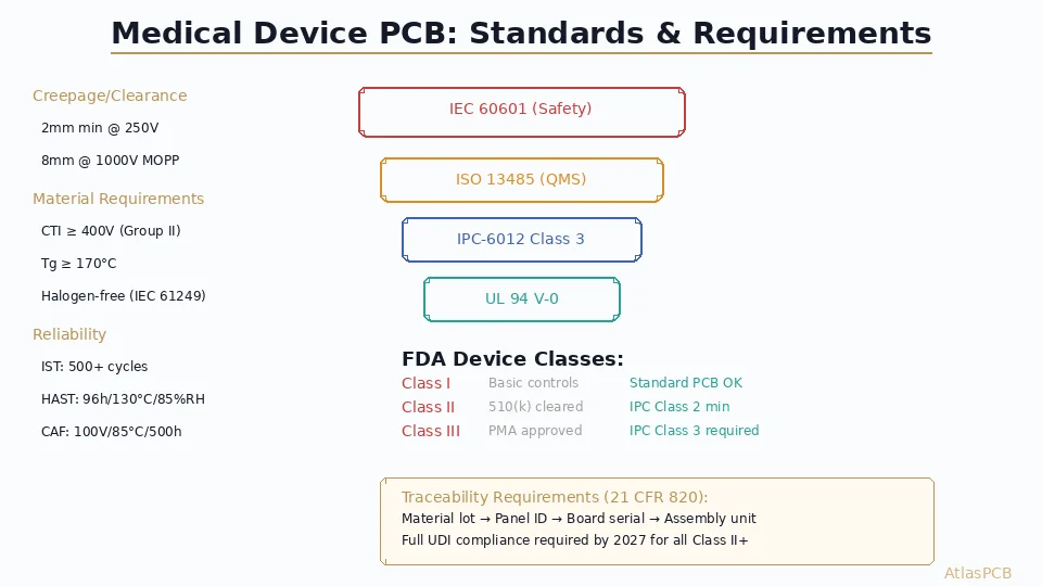
Medical Device PCB Requirements: IEC 60601, Creepage, and Reliability Standards You Cannot Skip
A manufacturing-focused guide to PCB requirements for medical devices. Covers the specific fabrication parameters driven by IEC 60601 safety standards, FDA device classification, creepage/clearance rules, material qualifications, and reliability testing requirements that determine whether your PCB passes regulatory review.
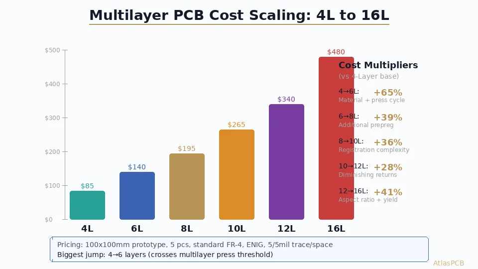
Multilayer PCB Cost: Why 6-Layer Costs 65% More Than 4-Layer (and How to Optimize)
Detailed cost analysis of multilayer PCBs from 4 to 16 layers with actual pricing data. Understand the specific manufacturing steps that drive each cost jump, and learn which design decisions reduce per-board cost by 15-40% without sacrificing electrical performance.
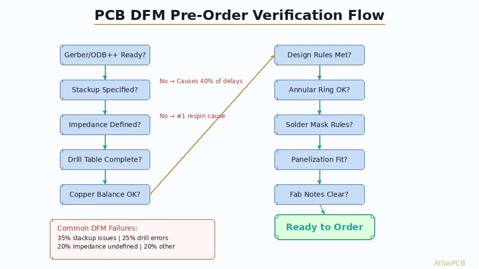
PCB DFM Check: The 10-Point Pre-Order Verification That Prevents 80% of Fabrication Delays
A systematic DFM verification checklist covering the specific items that cause fabrication holds, requotes, and delivery delays. Based on real data from 10,000+ orders — these are the issues manufacturers actually encounter, not theoretical possibilities.
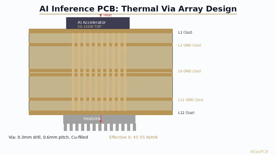
PCB Thermal Design for AI Inference Accelerators: Managing 50-150W in Edge Deployments
AI inference hardware pushes PCB thermal management beyond standard techniques. This guide covers the specific stackup, via, and material strategies needed for AI accelerator boards dissipating 50-150W without server-class cooling infrastructure.
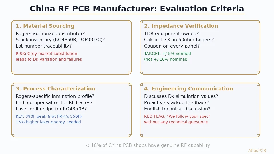
China RF PCB Manufacturer: Selection Guide for International Hardware Teams
How to evaluate and select a China-based RF PCB manufacturer for Rogers, PTFE, and hybrid stackups. Covers qualification criteria, communication expectations, common pitfalls, and what separates a capable RF house from a standard PCB shop quoting Rogers material.
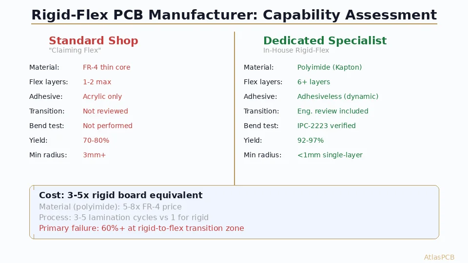
Rigid-Flex PCB Manufacturer: How to Evaluate Capability, Cost, and Reliability for Your Project
Selecting a rigid-flex PCB manufacturer requires verifying specific capabilities most standard shops lack. This guide covers the qualification criteria, cost drivers, design-for-manufacturing rules, and what separates a capable rigid-flex house from a standard PCB shop claiming flex capability.
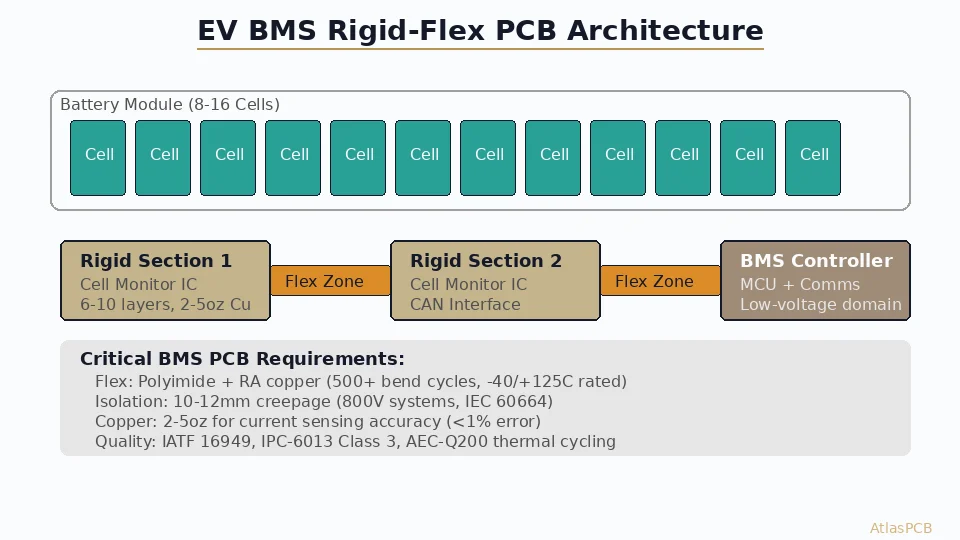
EV Battery Management System PCB: Rigid-Flex Design and Manufacturing Requirements
Electric vehicle BMS PCBs demand rigid-flex construction, high-voltage isolation, and automotive-grade reliability. This guide covers the specific PCB manufacturing requirements for BMS applications — from material selection and copper weight planning to IATF 16949 compliance and thermal cycling endurance.
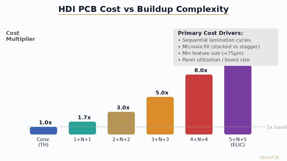
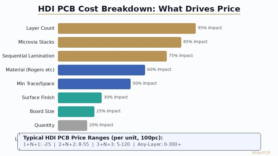
HDI PCB Cost Breakdown: Pricing Factors, Layer Count Impact, and Budget Optimization
What does an HDI PCB actually cost? Detailed pricing analysis covering microvia count, sequential lamination cycles, buildup configuration (1+N+1 through 5+N+5), material selection, and practical strategies to reduce HDI cost by 20-40% without sacrificing performance.
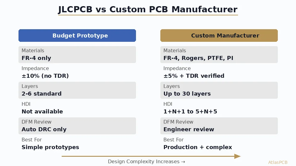
JLCPCB vs Custom PCB Manufacturer: When Budget Prototyping Falls Short
Comparing JLCPCB's automated low-cost model against dedicated custom PCB manufacturers. Understand where each excels — from $2 prototypes to controlled-impedance RF boards — and how to choose based on your project's actual requirements.
Rogers 4350B PCB Stackup Design: Layer Configuration, Hybrid Builds, and Manufacturing Specs
Complete engineering guide to Rogers RO4350B stackup design. Covers 4-layer to 10-layer configurations, hybrid Rogers/FR-4 builds, prepreg selection, copper weight planning, and the manufacturing constraints that determine whether your stackup is actually producible.
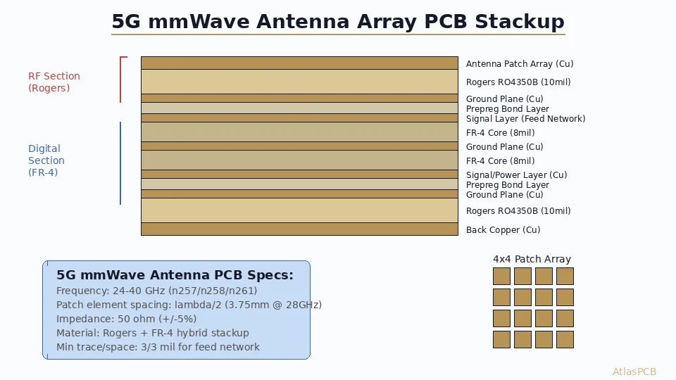
5G Antenna PCB Fabrication: mmWave Array Design and Manufacturing Challenges
Building 5G mmWave antenna arrays demands PCB fabrication precision most shops cannot deliver. Learn the material selection, stackup design, etching tolerances, and manufacturing process requirements for 24-40 GHz antenna PCBs.
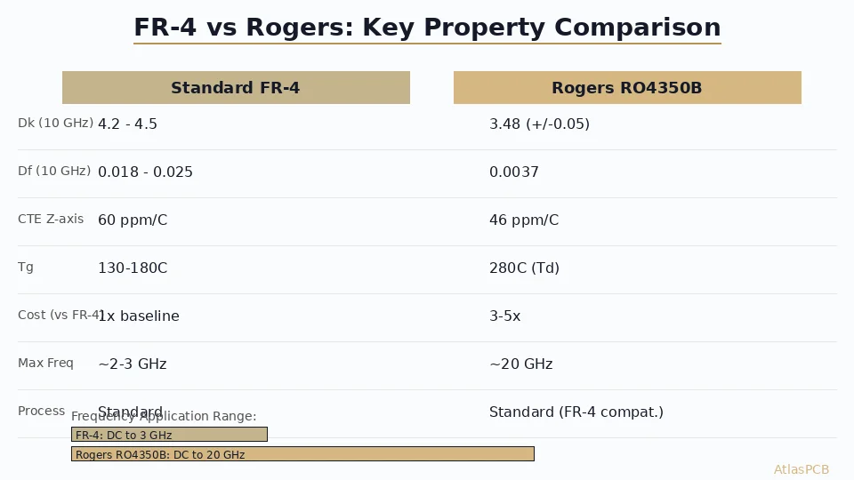
FR-4 vs Rogers PCB: Complete Material Selection Guide for RF and High-Speed Design
FR-4 or Rogers? Compare dielectric loss, thermal stability, cost, and fabrication compatibility to choose the right PCB material for your frequency range and budget constraints.
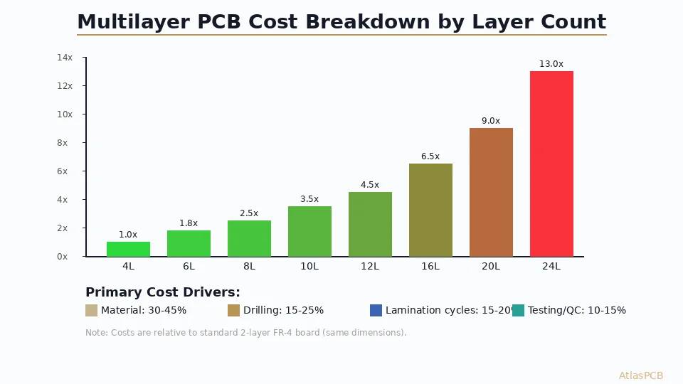
Multilayer PCB Cost Breakdown: What Drives Your Quote from 4 to 30 Layers
Understand exactly what drives multilayer PCB pricing. We break down cost factors by layer count — material, drilling, lamination cycles, testing — and show optimization strategies that can reduce your bill by 20-40%.
PCB DFM Check: The Complete Pre-Order Verification Guide for Engineers
Run a thorough PCB DFM check before ordering to avoid costly respins. This guide covers the critical design-for-manufacturability rules, common violations we catch, and how to verify your Gerber files are production-ready.
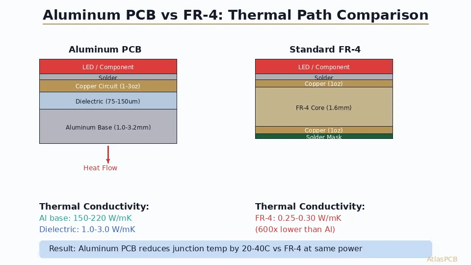
Aluminum PCB vs FR-4 for Thermal Management: Which Base Material Wins for LED and Power Designs?
Head-to-head comparison of aluminum-backed PCBs versus standard FR-4 for thermal management in LED lighting, power converters, and motor drives. Covers thermal conductivity, cost, reliability, and the design scenarios where each material is the right choice.
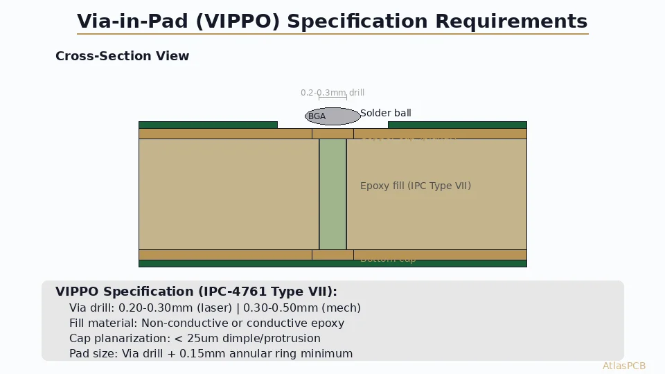
How to Specify Via-in-Pad on Your PCB Fab Drawing: VIPPO Requirements, IPC-4761, and DFM Checklist
Complete guide to specifying via-in-pad plated over (VIPPO) on your fabrication drawing. Covers IPC-4761 fill types, dimensional requirements, common DFM errors, and the exact notes your fab drawing needs for reliable via-in-pad production.
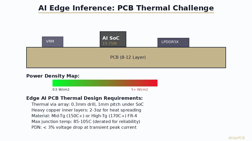
PCB Thermal Design for AI Edge Inference Accelerators: Managing 15-75W in Compact Form Factors
Engineering guide to PCB thermal management for edge AI inference hardware. Covers power delivery network design, thermal via arrays, material selection, and stackup optimization for AI SoCs dissipating 15-75W in space-constrained edge deployments without server-class cooling.
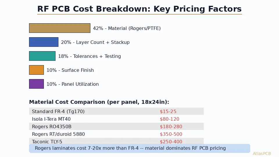
RF PCB Cost Breakdown: Why Rogers and High-Frequency Laminates Cost 7-20x More Than FR-4
Detailed pricing analysis of RF PCB fabrication costs, breaking down material, processing, tolerance, and testing surcharges. Covers Rogers RO4350B, RT/duroid, Taconic, and Megtron pricing with optimization strategies for budget-conscious RF engineers.
PCB Power Delivery Network Design for AI GPU Modules: VRM Layout, Copper Weight, and Decoupling Strategy
Engineering guide to designing PCBs that deliver 500-1000W to modern AI accelerator modules. Covers VRM placement strategy, copper weight selection for power planes, decoupling capacitor optimization, and thermal-aware PDN layout for GPU/TPU carrier boards.
How to Evaluate a PCB Manufacturer Before Sending Your RFQ: Capability Checklist for Complex Boards
Practical checklist for evaluating PCB fabricators before committing your HDI, RF, or multilayer design. Covers capability verification, quality certifications, communication red flags, and the questions that separate capable shops from those that will waste your time.
Citi Raises AI-PCB Market Forecast to RMB 562 Billion by 2028: Google TPU Demand Set to Surpass Nvidia
Citibank's June 2026 report raises its AI-PCB total addressable market forecast significantly, projecting RMB 562 billion by 2028 with 83% year-over-year growth. Analysis of what Google TPU dominance, optical module PCB surges, and capacity constraints mean for PCB buyers and fabricators.
PCB Small-Batch Pricing: How Volume Affects Unit Cost from 5 to 500 Pieces
Transparent analysis of PCB unit pricing across small production volumes. Understand the NRE-to-unit-cost crossover, optimal order quantities for each board complexity, and strategies to minimize per-piece cost without committing to mass production.
Rigid-Flex PCB vs FPC + Board-to-Board Connectors: Making the Right Interconnect Decision
Technical comparison of rigid-flex PCBs versus flexible flat cables with board-to-board connectors. Covers reliability, cost crossover points, assembly yield, and design scenarios where each approach wins.
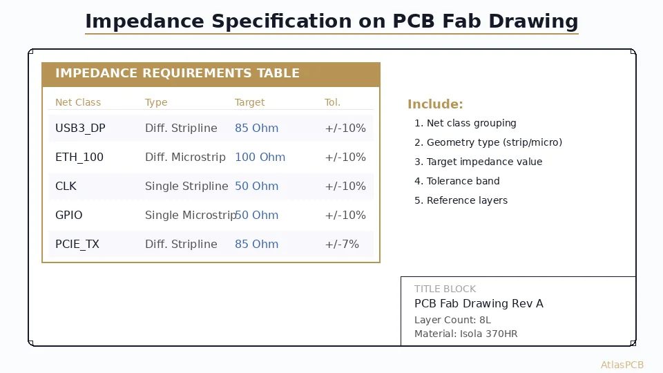
How to Specify Controlled Impedance on Your PCB Fab Drawing: A Complete DFM Guide
Step-by-step guide for specifying impedance requirements on your fabrication drawing, including table format, tolerance callouts, reference layers, and common mistakes that cause re-spins.
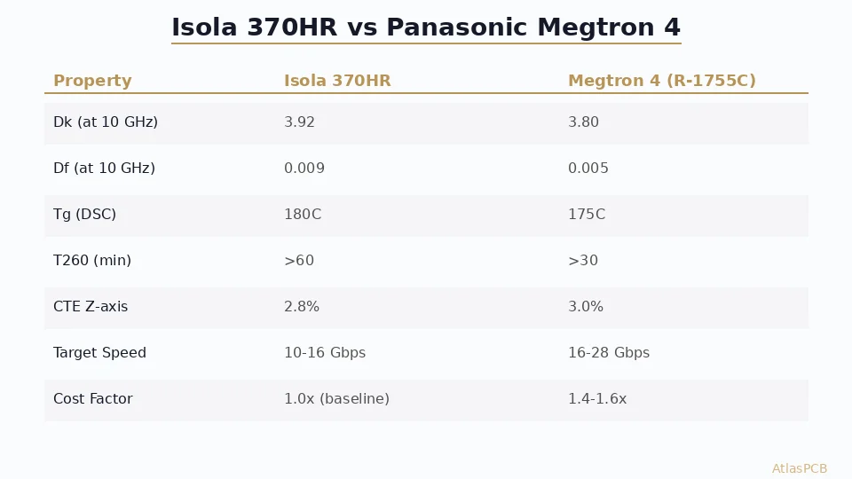
Isola 370HR vs Panasonic Megtron 4: Mid-Loss Laminate Selection for 10-25 Gbps Designs
A practical comparison of Isola 370HR and Panasonic Megtron 4 (R-1755C) for mid-speed digital designs, covering Dk/Df, thermal reliability, cost, and real-world use cases.
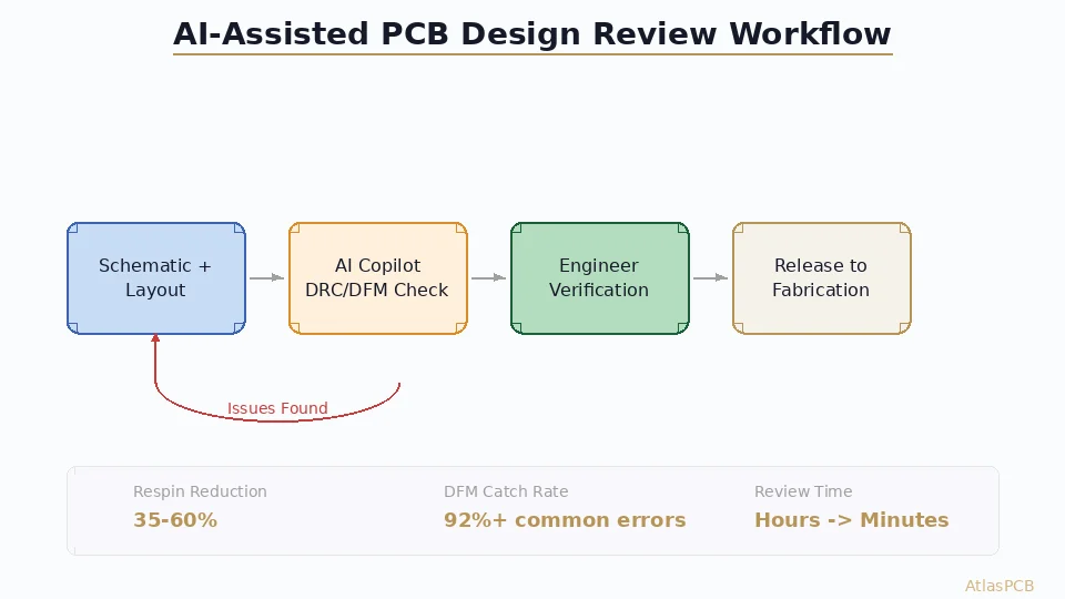
LLM-Assisted PCB Design Review: How AI Copilots Are Reducing Respins in 2026
Practical assessment of AI/LLM-powered design review tools for PCB engineers — what works today, what does not, and how to integrate AI copilots into your DFM workflow without over-trusting automation.
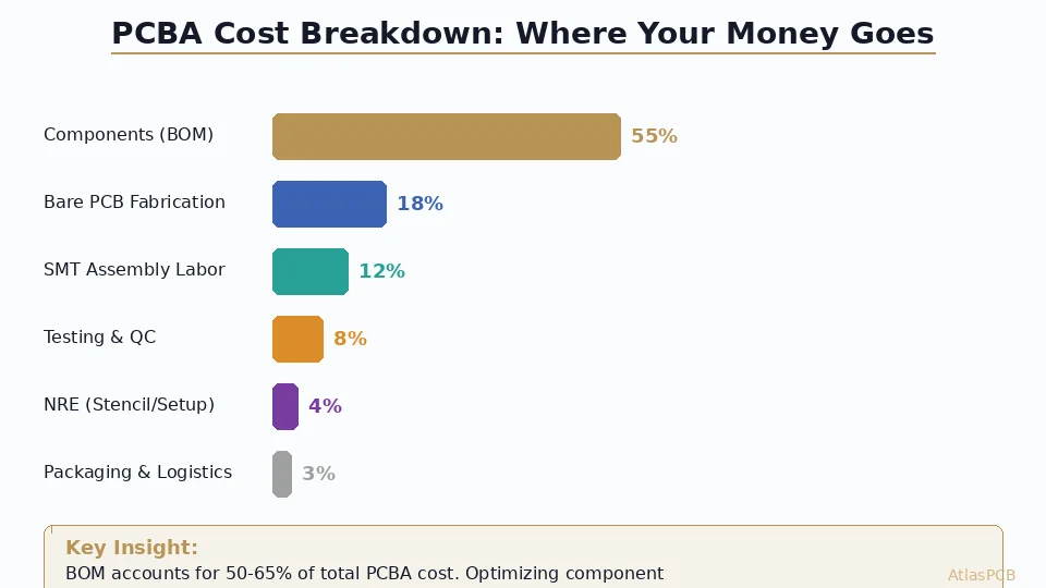
PCBA Cost Breakdown 2026: Understanding BOM, Assembly, NRE, and Testing Charges
Transparent breakdown of PCB assembly costs — where your money actually goes, what drives each cost element, and practical strategies to reduce your per-unit PCBA price without sacrificing quality.
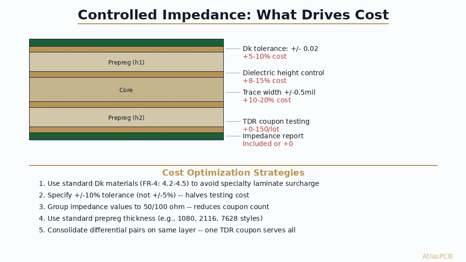
Controlled Impedance PCB Pricing: What It Costs and How to Optimize Your Stackup
Detailed breakdown of controlled impedance PCB cost factors — from material selection and dielectric tolerance to TDR testing and coupon design. Learn which impedance specs actually need premium tolerances and where you can save 15-30% by specifying smarter.
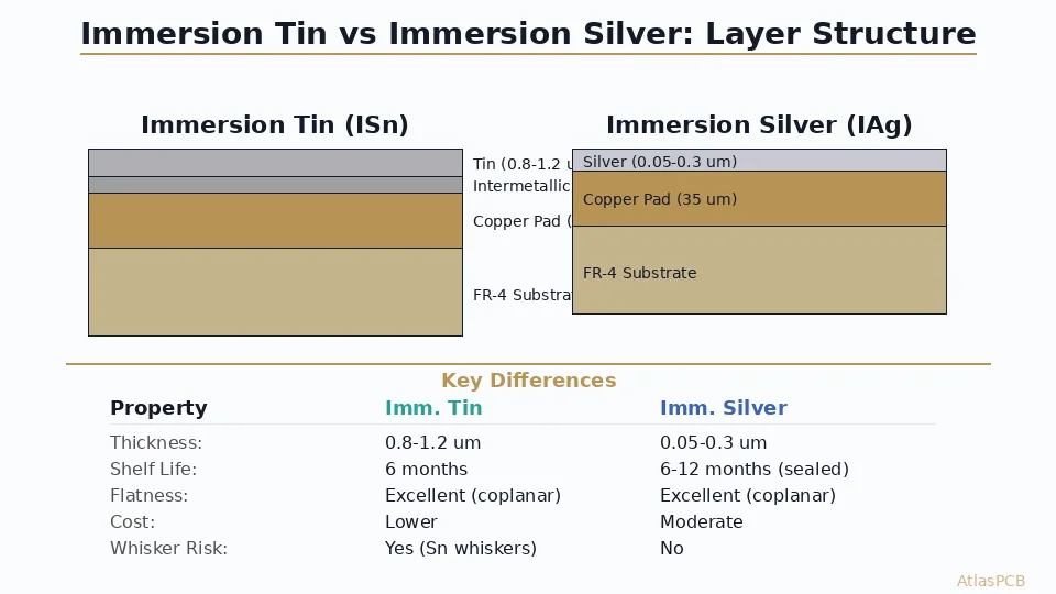
Immersion Tin vs Immersion Silver: PCB Surface Finish Selection for Solderability and Shelf Life
A direct engineering comparison of immersion tin and immersion silver surface finishes — covering cost, shelf life, solderability, signal integrity, and failure modes. Includes decision matrix for choosing between ISn and IAg based on your assembly process, storage constraints, and reliability requirements.
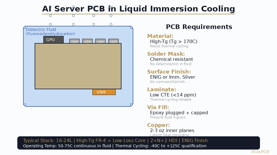
Liquid Cooling Compatible PCB Design for AI Data Centers: Material and Reliability Requirements
Engineering guide for designing PCBs that survive immersion cooling environments in AI data centers. Covers material compatibility with dielectric fluids, thermal cycling reliability, solder mask chemical resistance, via fill requirements, and stackup considerations for 800W+ GPU server boards operating in single-phase and two-phase liquid cooling systems.
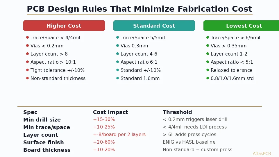
PCB Design Rules for Minimum Fabrication Cost: A DFM Guide for Engineers Ordering Boards
Practical DFM guidelines that directly reduce PCB fabrication price. Covers trace/space thresholds, drill sizes, layer count decisions, material selection, and panelization strategies that keep your board in standard manufacturing processes and away from premium pricing tiers.
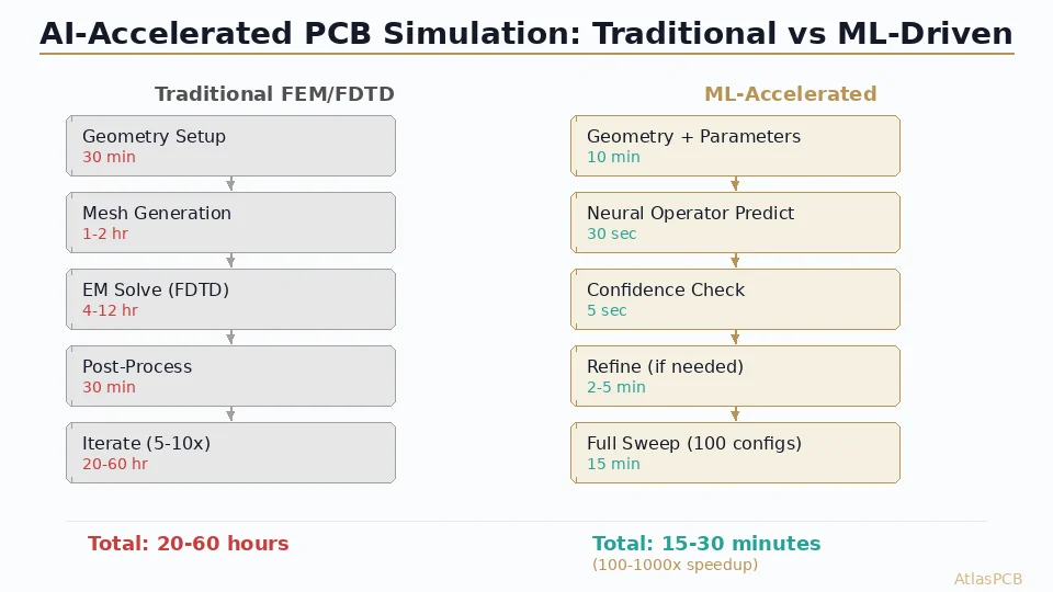
AI-Accelerated PCB Simulation: How Machine Learning Transforms SI/PI Analysis and Thermal Modeling
How neural operators and ML surrogate models are replacing traditional FEM/FDTD simulation for PCB signal integrity, power integrity, and thermal analysis — delivering 100-1000x speedups that enable real-time design optimization.
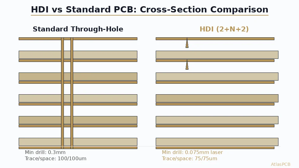
HDI PCB vs Standard Through-Hole: Design Tradeoffs, Cost, and When to Upgrade
Comparing HDI PCB technology against standard through-hole construction: routing density, signal integrity, cost per layer, and decision criteria for engineers choosing between conventional and HDI fabrication.
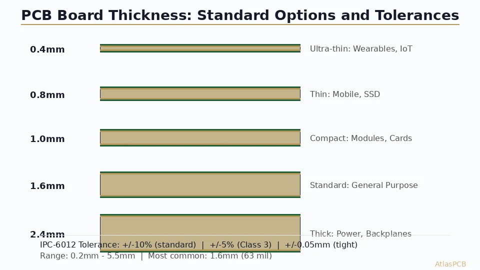
How to Specify PCB Board Thickness: Standard Options, Tolerances, and Fab Drawing Requirements
Complete guide to specifying PCB board thickness in your fabrication drawing. Covers standard thickness values, IPC tolerance classes, stackup-driven thickness control, and common mistakes that delay quotes.
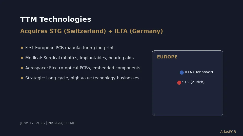
TTM Technologies Acquires Swiss Technology Group and ILFA: European PCB Expansion for Medical and Aerospace
TTM Technologies announces acquisition of Swiss Technology Group AG and ILFA GmbH, establishing its first European manufacturing presence with specialized capabilities in miniaturized medical PCBs, electro-optical boards, and embedded components.
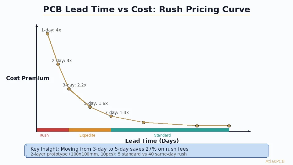
PCB Rush Pricing Explained: Lead Time vs Cost Tradeoffs for Prototypes and Production
Understanding PCB rush pricing mechanics: how lead time affects fabrication cost, where the money actually goes in expedited orders, and strategies to minimize rush fees without delaying your project timeline.
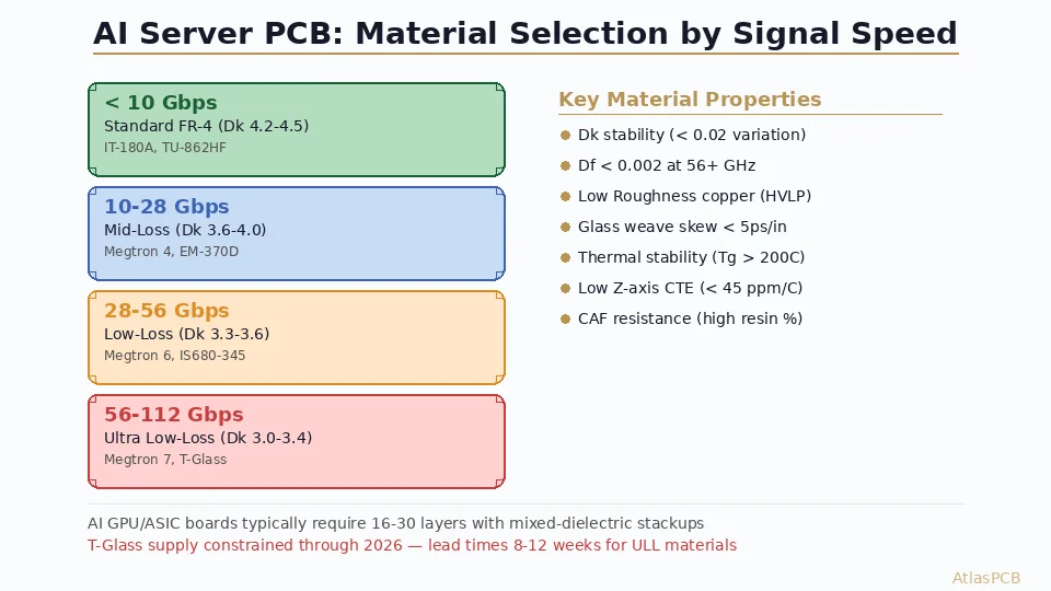
AI Server PCB Material Selection: T-Glass, Megtron 7, and the Low-Loss Laminate Supply Crisis
Engineering guide to PCB material selection for AI server and GPU accelerator boards operating at 56-112 Gbps per lane. Covers T-Glass shortage impact, Megtron 6/7 supply constraints, alternative ultra-low-loss laminates, mixed-dielectric stackup strategies, and how to secure materials for 16-30 layer AI compute boards in 2026.
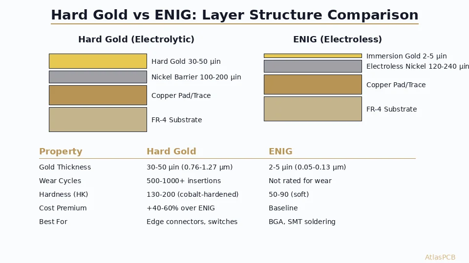
Hard Gold vs ENIG for PCB Connectors: Choosing the Right Finish for Edge Contacts and Card Slots
Compare hard gold (electrolytic) and ENIG surface finishes for PCB edge connectors, gold fingers, and card-edge contacts. Covers wear resistance, gold thickness, insertion cycles, cost impact, and specification guidelines for PCI Express, DDR DIMM, and industrial card-edge applications.
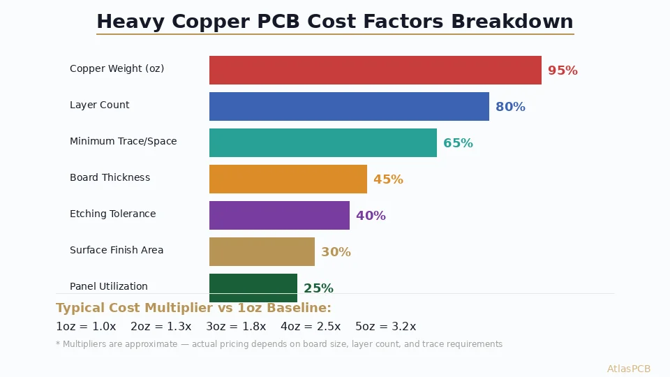
Heavy Copper PCB Cost Breakdown: What Drives Pricing for 2oz-5oz Power Boards
Detailed cost analysis of heavy copper PCB fabrication covering 2oz through 5oz designs. Breaks down how copper weight, etching challenges, minimum trace/space, layer count, and board thickness affect pricing. Includes cost multipliers, optimization strategies, and when heavy copper makes financial sense vs alternative approaches.
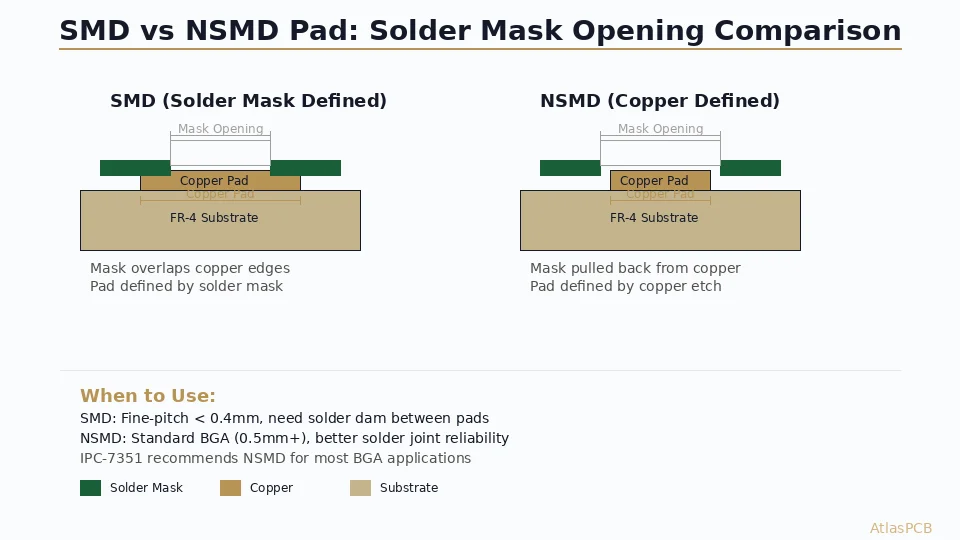
SMD vs NSMD Pad Design: How to Specify Solder Mask Openings for BGA and Fine-Pitch Components
Complete engineering guide to solder mask defined (SMD) vs non-solder mask defined (NSMD) pad design for BGA, QFN, and fine-pitch components. Covers pad geometry rules, IPC-7351 guidelines, thermal fatigue life comparison, solder joint reliability data, and how to specify mask openings in your Gerber output.
PCB Design for AI Edge Inference: Thermal, Power Delivery, and Signal Integrity Challenges
Engineering guide for PCB designers building AI edge inference hardware. Covers thermal management for NPUs, power delivery network design for transient AI workloads, and high-speed memory interface routing for edge ML accelerators.
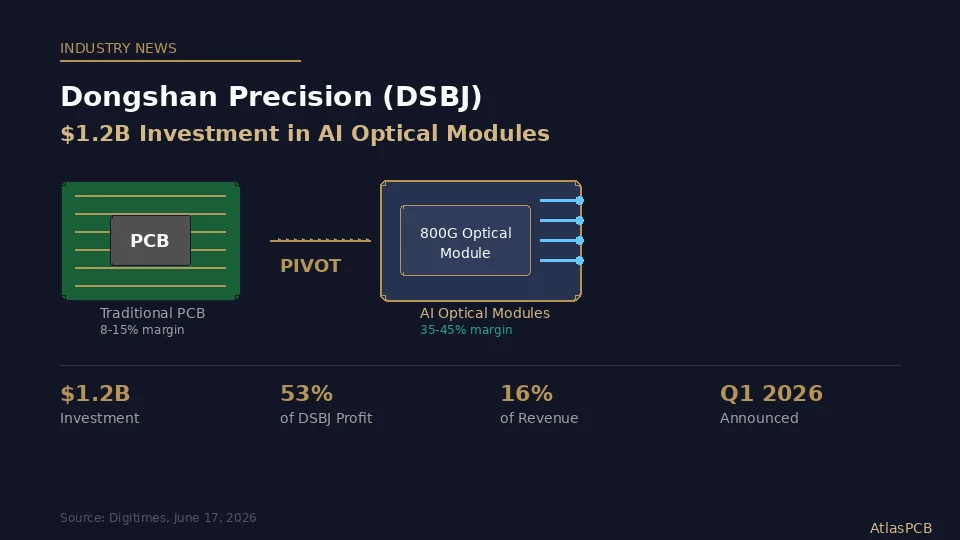
Dongshan Precision (DSBJ) Invests $1.2B in AI Optical Modules: PCB Maker Pivots to Photonics
China's Dongshan Precision announces $1.2 billion expansion into AI optical chip and module production through subsidiary Source Photonics. What this means for PCB supply chain capacity and the growing convergence of PCB manufacturing and optical interconnects.
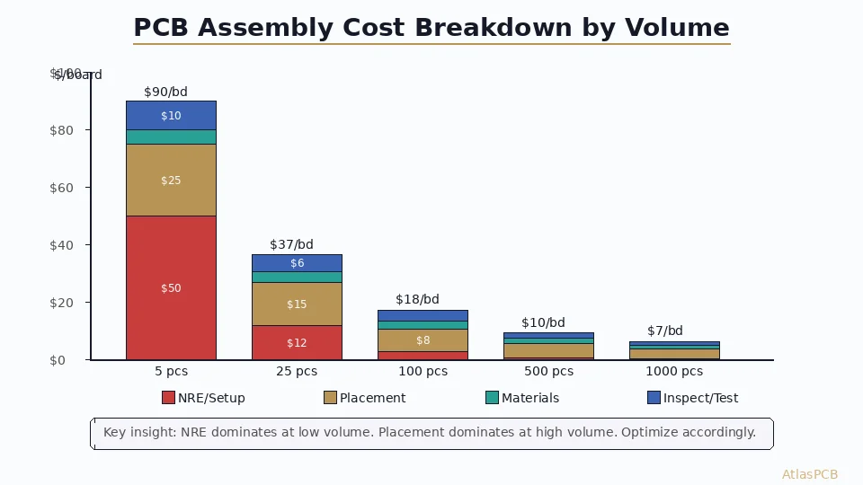
PCB Assembly Cost Breakdown: PCBA Pricing Factors and Optimization Guide
Understand what drives PCB assembly costs: component placement, solder paste, reflow profiles, inspection, and test. Detailed cost breakdown with optimization strategies for prototype and production volumes.
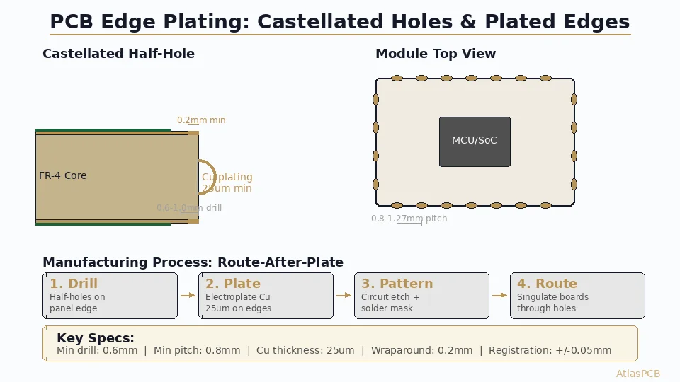
How to Specify PCB Edge Plating: Fab Drawing Requirements and DFM Rules
Complete specification guide for PCB edge plating (castellated edges, plated board edges). Includes fab note examples, dimensional tolerances, design rules, and common DFM failures to avoid.
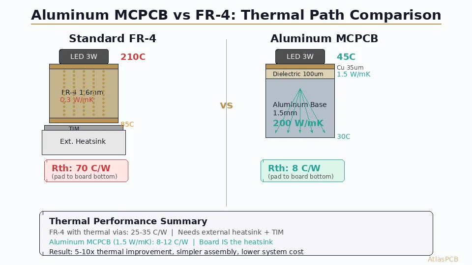
Aluminum PCB vs FR-4: When Metal-Core Makes Sense for Thermal Management
Compare aluminum MCPCB and standard FR-4 for LED, power electronics, and motor driver applications. Thermal conductivity data, cost trade-offs, and design rules for choosing the right substrate.
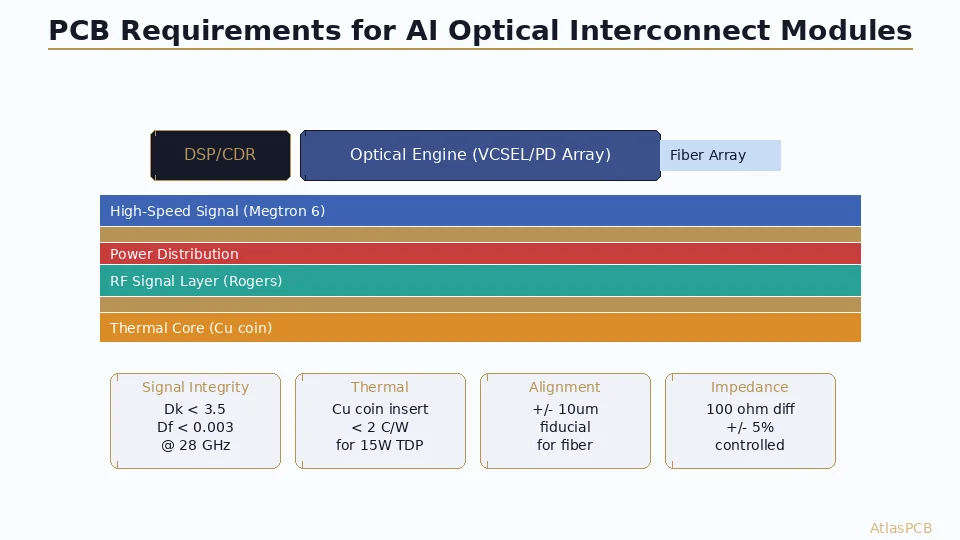
PCB Design for AI Optical Interconnect Modules: Material, Thermal, and Signal Integrity Requirements
Engineering guide to PCB substrate requirements for co-packaged optics and optical transceiver modules in AI data center infrastructure. Covers low-loss laminate selection, thermal management for VCSEL/driver ICs, and 56 GBaud signal integrity.
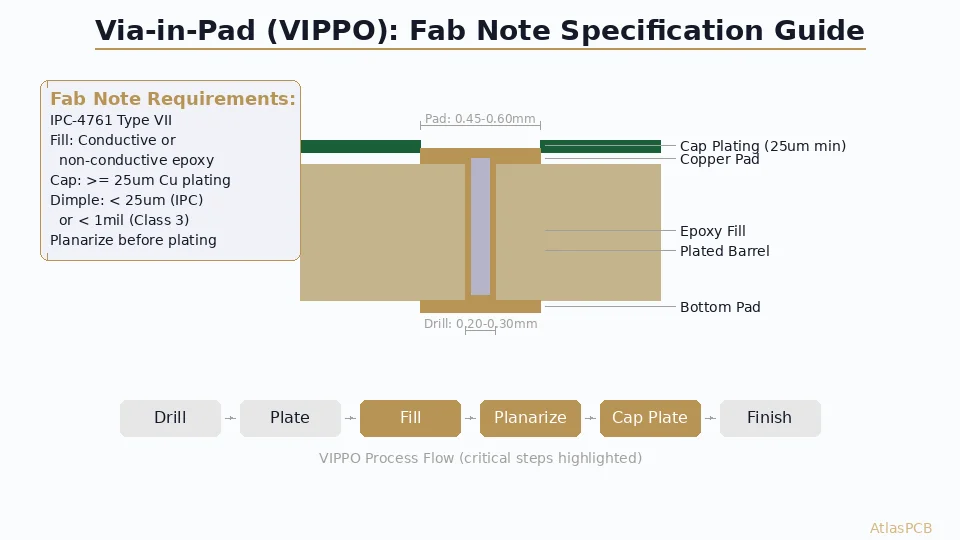
How to Specify Via-in-Pad (VIPPO) in PCB Fab Notes: Complete DFM Guide
Step-by-step guide to specifying via-in-pad plated over (VIPPO) in your fabrication drawings. Covers IPC-4761 types, fill materials, cap plating requirements, dimple tolerances, and common fab note mistakes that cause production delays.
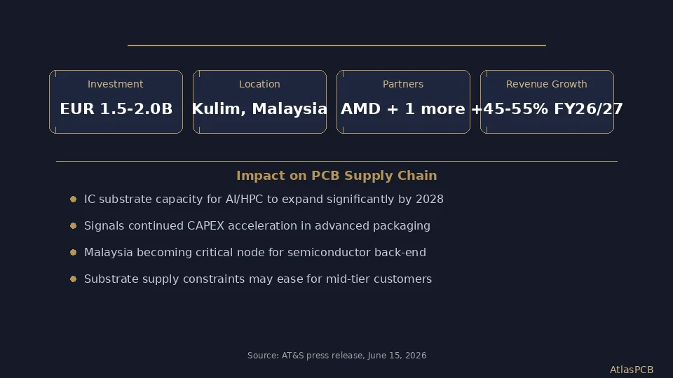
AT&S Invests EUR 2 Billion in Malaysia AI Substrate Expansion — What It Means for PCB Buyers
AT&S announces EUR 1.5-2.0 billion investment in Kulim, Malaysia for AI substrate capacity with AMD partnership. Analysis of supply chain impact, substrate availability timeline, and implications for PCB procurement in 2026-2028.
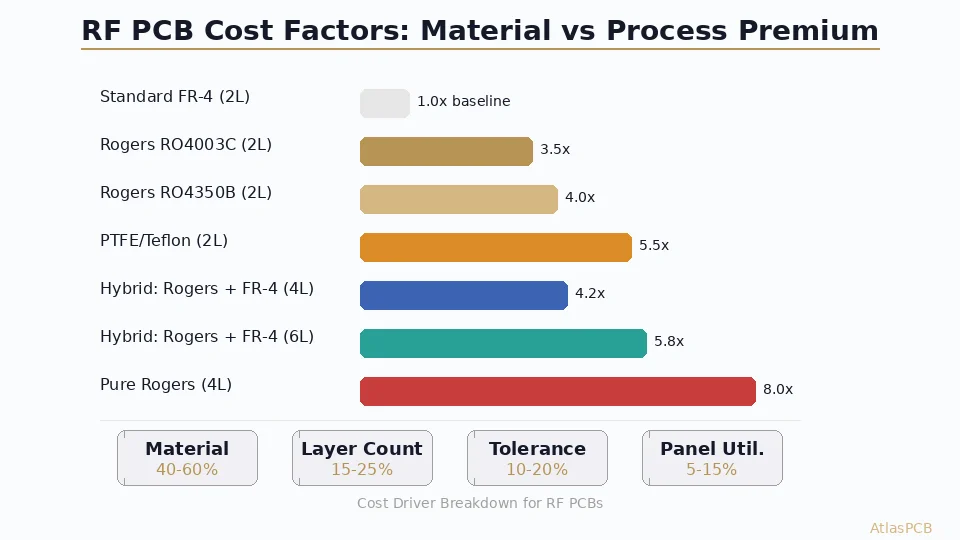
RF PCB Cost Breakdown: Rogers, PTFE, and Hybrid Stackup Pricing Guide 2026
Understand what drives RF PCB manufacturing costs. Compare Rogers RO4350B, RO4003C, PTFE, and FR-4 hybrid stackup pricing with real cost multipliers, optimization strategies, and quotes.
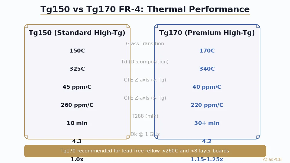
Tg150 vs Tg170 FR-4: Choosing the Right Glass Transition Temperature for Your PCB
Compare Tg150 and Tg170 FR-4 laminates for thermal reliability, lead-free assembly, and cost. Engineering decision guide with real CTE data, T288 ratings, and application recommendations.
NVIDIA HVLP4 Copper Foil Requirements: What Next-Gen AI Server PCBs Demand from Your Fabricator
NVIDIA is driving adoption of HVLP4 ultra-low-profile copper foil for AI server PCBs, creating a widening gap between fabricators who can source it and those who cannot. Technical analysis of why HVLP4 matters for 112G+ SerDes channels, what Rz roughness specifications mean for insertion loss, and how to specify copper foil grade in your PCB stackup.
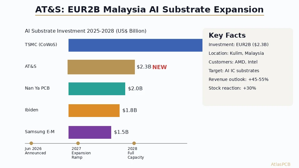
AT&S Invests EUR2 Billion in Malaysia AI Substrate Expansion: What It Means for PCB Supply Chains
Austrian IC substrate manufacturer AT&S announces EUR2 billion investment to expand Kulim, Malaysia facility for AI chip packaging. Backed by AMD and Intel commitments, this expansion addresses the global AI substrate bottleneck and signals continued tightening of advanced packaging capacity through 2028.
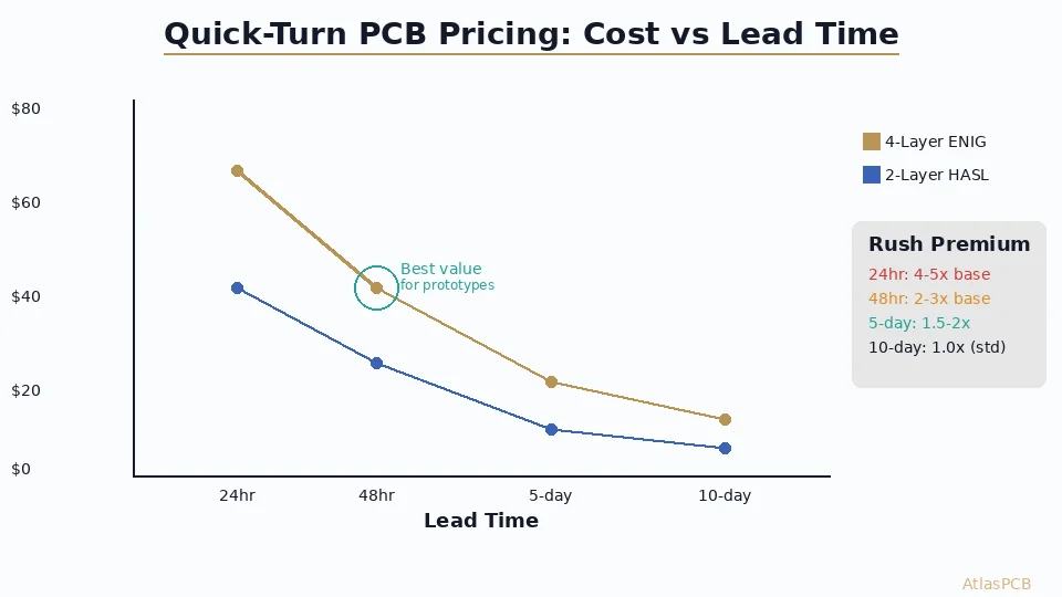
Quick-Turn PCB Pricing: What Express Lead Time Actually Costs and When It's Worth It
Transparent breakdown of quick-turn PCB pricing premiums. Covers rush fees for 24hr, 48hr, and 5-day express service across 2-layer to 16-layer boards. Includes cost-per-day analysis and decision framework for when express manufacturing makes financial sense.
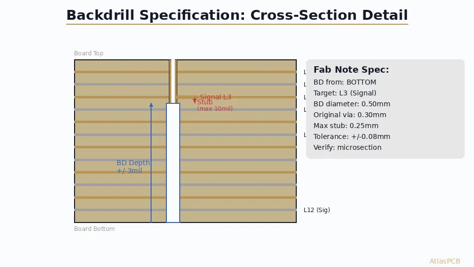
How to Specify Backdrilling in Your PCB Fab Notes: Depth, Tolerances, and Drawing Callouts
Complete guide to specifying backdrilling (controlled-depth drilling) in your PCB fabrication notes. Covers stub length calculations, depth tolerance callouts, drawing annotations, and common mistakes that cause signal integrity failures or manufacturing rejections.
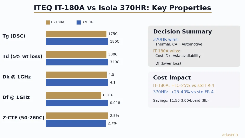
ITEQ IT-180A vs Isola 370HR: Mid-Tg Laminate Selection for High-Reliability PCBs
Direct comparison of ITEQ IT-180A and Isola 370HR laminates for high-reliability applications. Covers Tg, Td, CTE, Dk/Df, CAF resistance, and total cost impact. Decision framework for automotive, industrial, and telecom designs.
PCB Design Requirements for Edge AI Inference Modules: Thermal, Power Delivery, and Signal Integrity
Engineering guide covering PCB design requirements for edge AI inference modules — from NVIDIA Jetson and Google TPU edge boards to custom ASIC deployments. Covers power delivery network design, thermal via arrays, high-speed memory interfaces, and compact HDI stackups for AI at the edge.
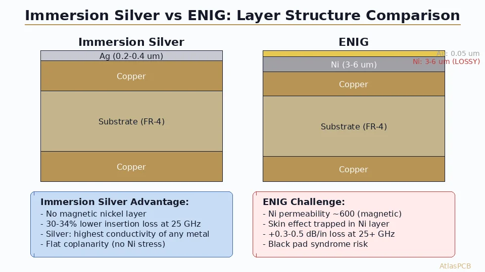
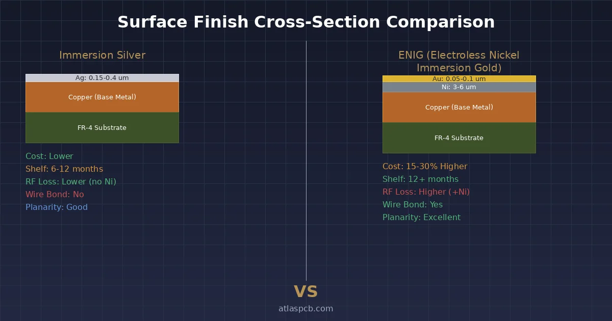
Immersion Silver vs ENIG for High-Speed PCB: Which Surface Finish Wins?
A direct comparison of Immersion Silver and ENIG surface finishes for high-speed digital applications. Covers signal loss, solderability, shelf life, cost, and when each finish is the right engineering choice.
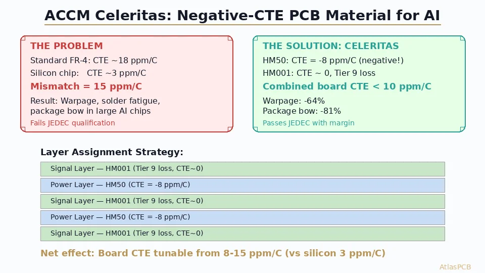
ACCM Launches Celeritas Negative-CTE PCB Material to Solve AI Chip Warpage and Signal Loss
Advanced Chip and Circuit Materials (ACCM) announces Celeritas HM50 and HM001 — purpose-built PCB laminates that eliminate warpage and high-frequency signal loss in large-format AI accelerator packages. What this means for high-layer-count board design.
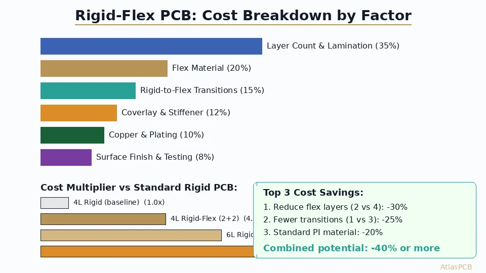
Rigid-Flex PCB Cost Breakdown: What Drives Pricing and How to Optimize Your Design for Budget
Transparent breakdown of rigid-flex PCB pricing factors. Learn exactly what costs $X per panel, how bend zone design affects price, and practical optimization strategies that cut 20-40% without compromising reliability.
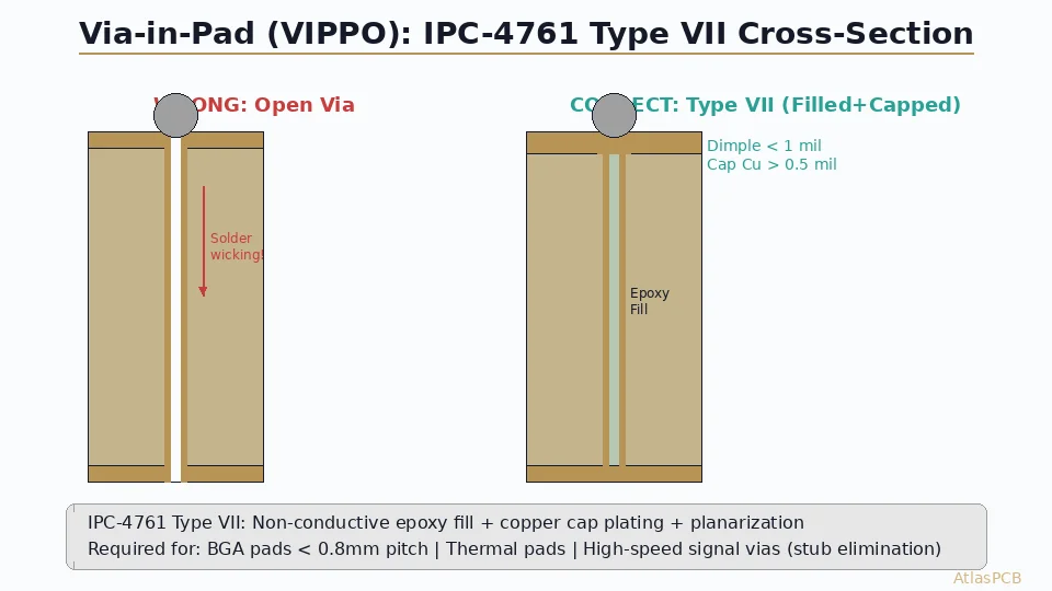
How to Specify Via-in-Pad for BGA Fanout: DFM Requirements and Fab Drawing Checklist
Complete DFM guide for specifying via-in-pad (VIPPO) on your PCB fab drawing. Covers hole sizes, plating fill requirements, cap plating thickness, IPC-4761 types, and the exact callouts your fabricator needs to build it right the first time.
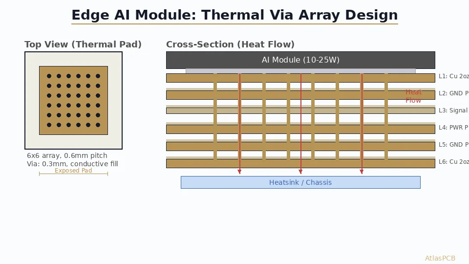
PCB Thermal Design for Edge AI Inference Modules: Copper Pour Strategy and Via Array Optimization
Practical thermal management guide for PCBs carrying edge AI inference modules (NVIDIA Jetson, Hailo-8, Google Coral). Covers thermal via array sizing, copper pour techniques, stackup considerations, and heat spreader integration for processors dissipating 5-25W in compact form factors.
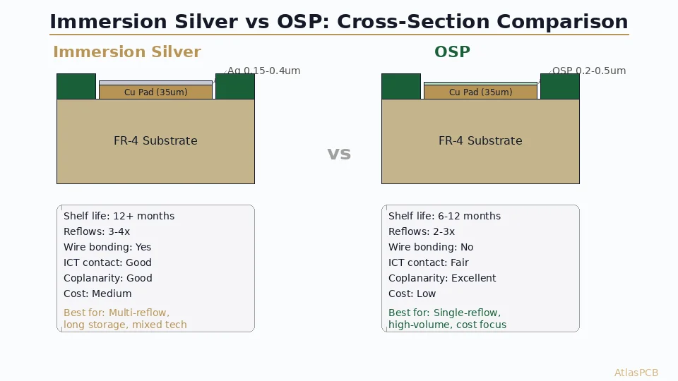
Immersion Silver vs OSP: Surface Finish Selection for High-Speed PCB Designs
Compare immersion silver and OSP surface finishes for high-speed digital and mixed-signal PCBs. Covers shelf life, solderability, signal integrity impact, cost, and decision criteria for choosing between these lead-free finishes.
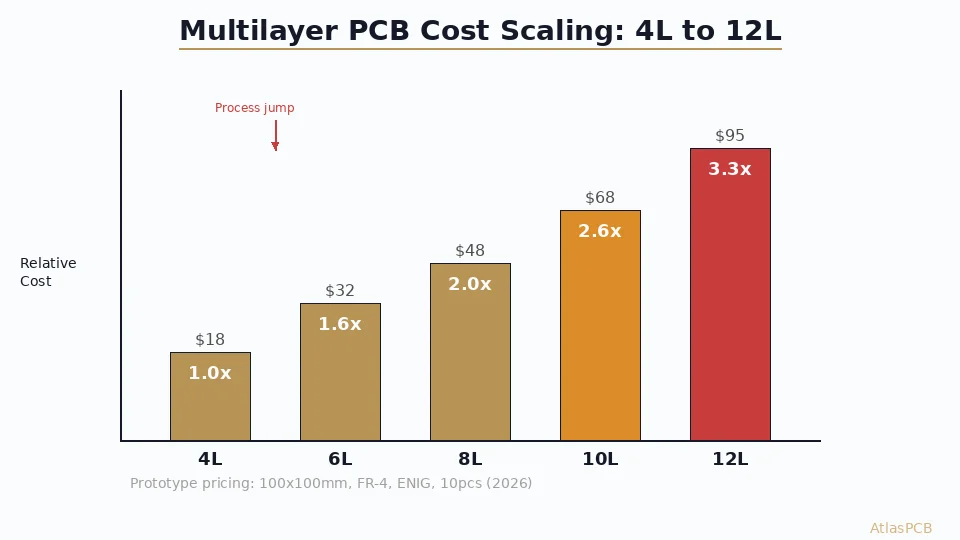
Multilayer PCB Cost: 4-Layer vs 6-Layer vs 8-Layer Price Comparison and Optimization
Detailed cost comparison between 4-layer, 6-layer, and 8-layer PCBs. Understand the real cost drivers — layer count, material selection, via structure, and minimum trace — with actual pricing ranges and strategies to reduce per-board cost without sacrificing performance.
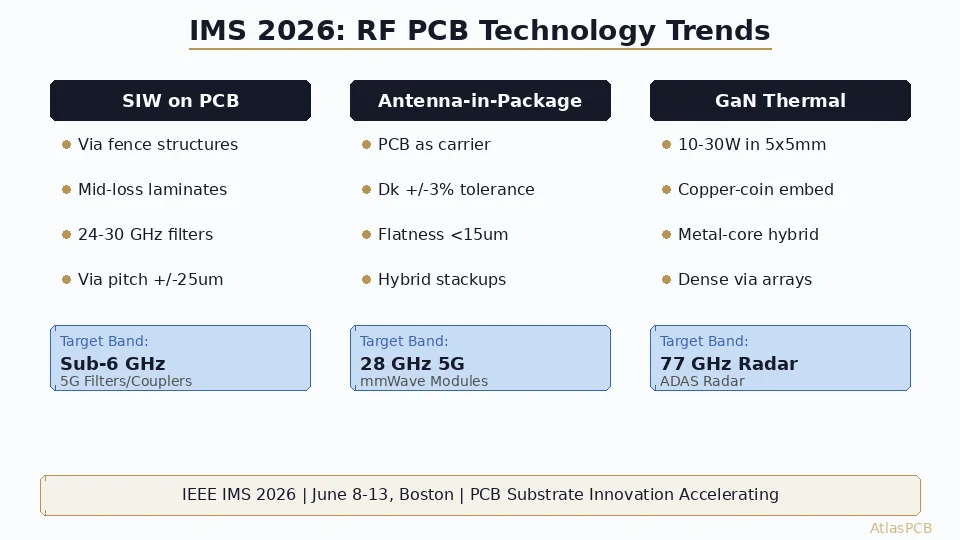
IMS 2026 Wrap-Up: RF PCB Technology Trends from the IEEE Microwave Symposium in Boston
Key RF and microwave PCB technology developments from IEEE IMS 2026 (June 8-13, Boston). Coverage of substrate-integrated waveguide advances, mmWave packaging trends, GaN-on-PCB integration, and what these developments mean for high-frequency board fabrication in 2026-2027.
PCB Lead Times Explained: What Drives Turnaround and How to Get Boards Faster
A fabricator's perspective on what actually determines PCB manufacturing lead time. Understand the production steps, common delays, and practical strategies to shorten delivery without compromising quality.
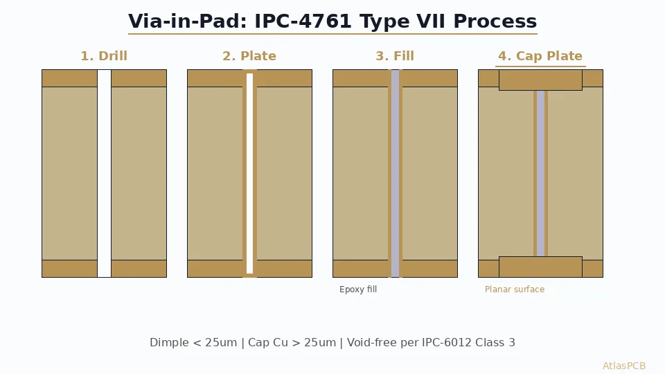
How to Specify Via-in-Pad: DFM Requirements, Fill Options, and Common Mistakes
Complete DFM guide for specifying via-in-pad (VIP) in your PCB design. Covers fill types (conductive vs non-conductive), plating requirements, IPC-4761 classifications, Gerber annotation, and the fabrication constraints that determine cost and yield.
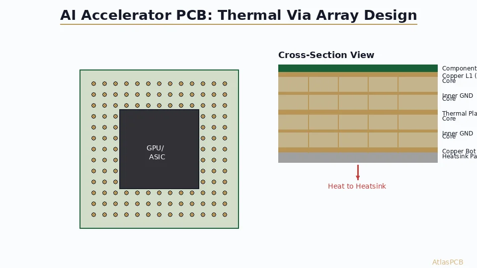
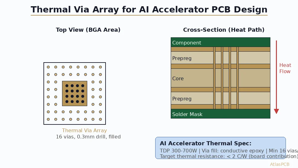
Thermal Management PCB Design for AI Accelerator Cards: PDN, Via Arrays, and Material Selection
Design guide for PCBs carrying AI GPUs and ASICs with 300-700W TDP. Covers thermal via arrays, power delivery network design, material selection for high-temperature operation, and heatsink interface optimization.
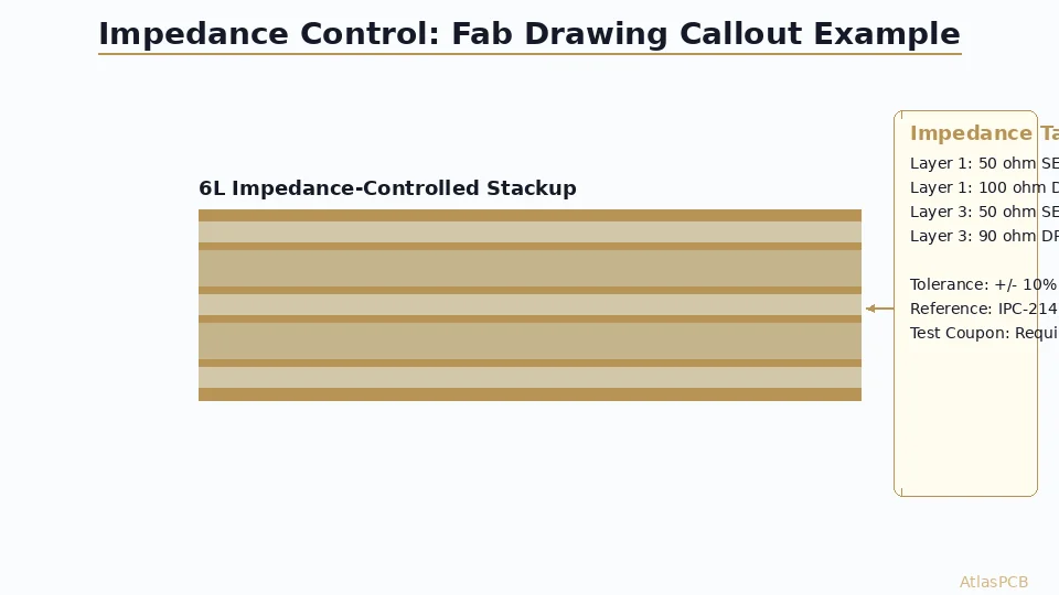
How to Specify Impedance Control on Your PCB Fab Drawing
Complete guide to specifying controlled impedance on PCB fabrication drawings. Includes impedance table format, tolerance callouts, coupon requirements, and common mistakes that cause DFM rejections.
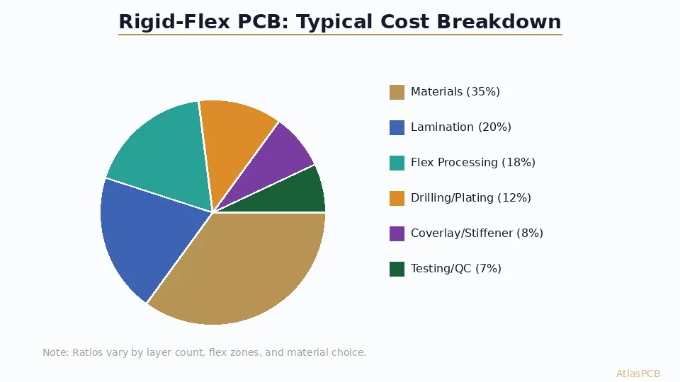
Rigid-Flex PCB Cost Breakdown: What Drives Pricing and How to Optimize
Understand what makes rigid-flex PCBs expensive and how to reduce cost by 20-40% through design optimization. Covers material, layer count, flex zones, stiffeners, and volume pricing.
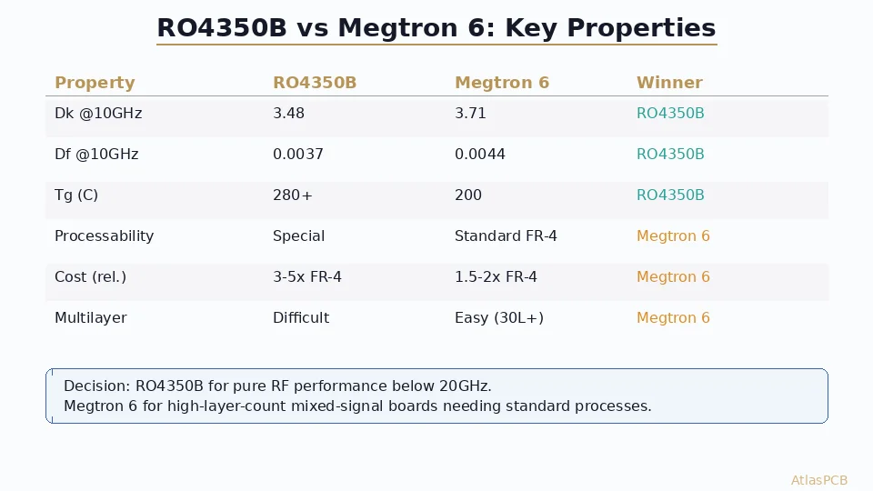
Rogers RO4350B vs Megtron 6: Which High-Frequency Laminate for Your Next Design?
A direct comparison of Rogers RO4350B and Panasonic Megtron 6 for RF, 5G, and high-speed digital applications. Dk, Df, processability, cost, and when to choose each.
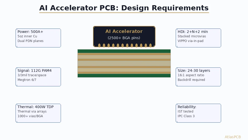
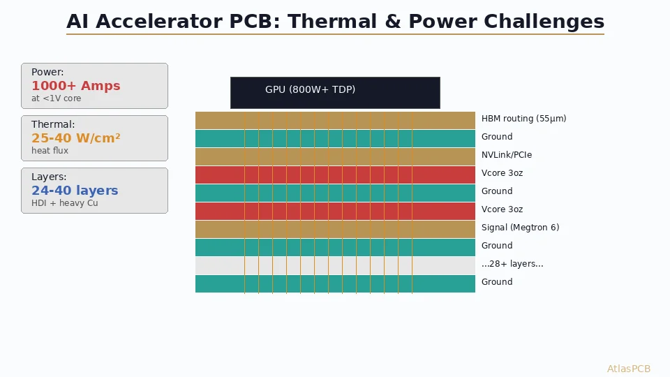
PCB Requirements for AI Accelerator Hardware: Layer Count, Power Delivery, and Thermal Design
Designing PCBs for AI accelerators (GPUs, TPUs, custom ASICs) demands extreme specifications: 20-30 layers, 500A+ current delivery, 3/3mil routing, and advanced thermal management. Here's what your fabricator needs to deliver.
HDI PCB Cost Breakdown: What Drives Pricing and How to Optimize Your Budget
Understand exactly what makes HDI PCBs expensive and where you can save money without sacrificing performance. Real pricing data for 1+N+1 through 5+N+5 buildups with cost optimization strategies.
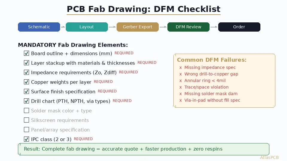
PCB Fab Drawing Requirements: The Complete DFM Specification Checklist for First-Time-Right Manufacturing
Your Gerber files are only half the story. Learn exactly what information your PCB fab drawing must contain to avoid misquotes, manufacturing errors, and costly respins. Includes downloadable checklist.
Rogers RO4350B vs PTFE for RF PCB: Material Selection Guide for 5G, Radar, and mmWave
Choosing between Rogers RO4350B and PTFE for your RF PCB? Compare dielectric properties, thermal reliability, fabrication compatibility, and cost to make the right material decision for your frequency range.
PCB Thermal Design for AI Inference Accelerators: Via Arrays, Copper Planes, and HDI Stackup Strategies
Engineering guide to PCB thermal management for AI inference hardware. Covers thermal via array design, copper plane allocation, HDI stackup optimization for 200-700W TDP AI chips, and material selection for sustained thermal cycling.
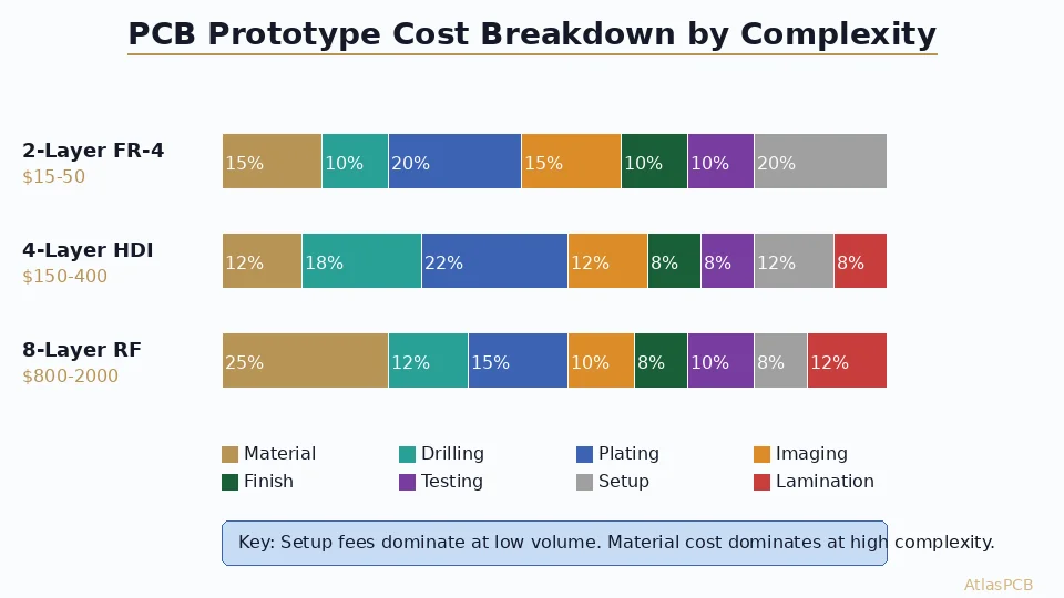
PCB Prototype Cost Breakdown: What Drives Price and How to Save 30-50% on First Runs
Transparent breakdown of PCB prototype pricing: setup fees, material costs, drilling, plating, and testing. Learn what drives cost at low volumes and how to optimize your prototype order for maximum value.
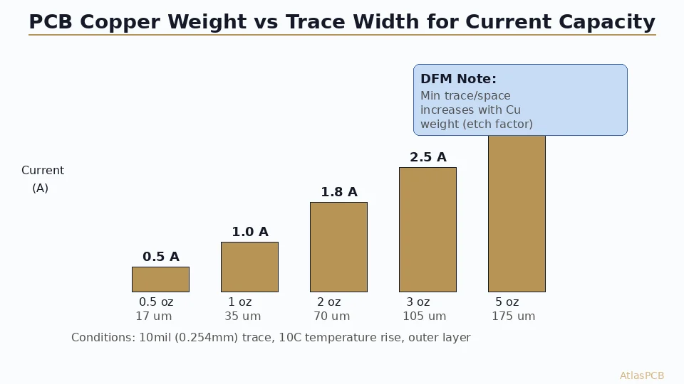
How to Specify PCB Copper Weight: Current Capacity, Etching Limits, and Stackup Rules
Complete guide to specifying copper weight in PCB fabrication drawings. Covers current capacity calculations, etch factor constraints on trace width, inner vs outer layer differences, and cost implications from 0.5oz to 5oz copper.
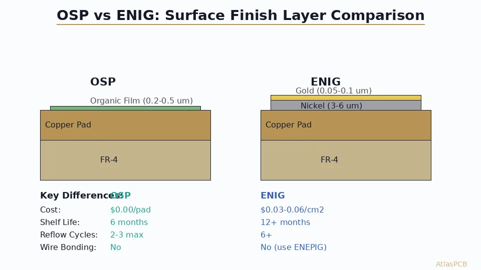
OSP vs ENIG Surface Finish: Cost, Shelf Life, and Assembly Decision Guide
Direct comparison of OSP and ENIG surface finishes for PCB manufacturing. Covers cost per pad, shelf life, reflow compatibility, and when each finish makes engineering and commercial sense.
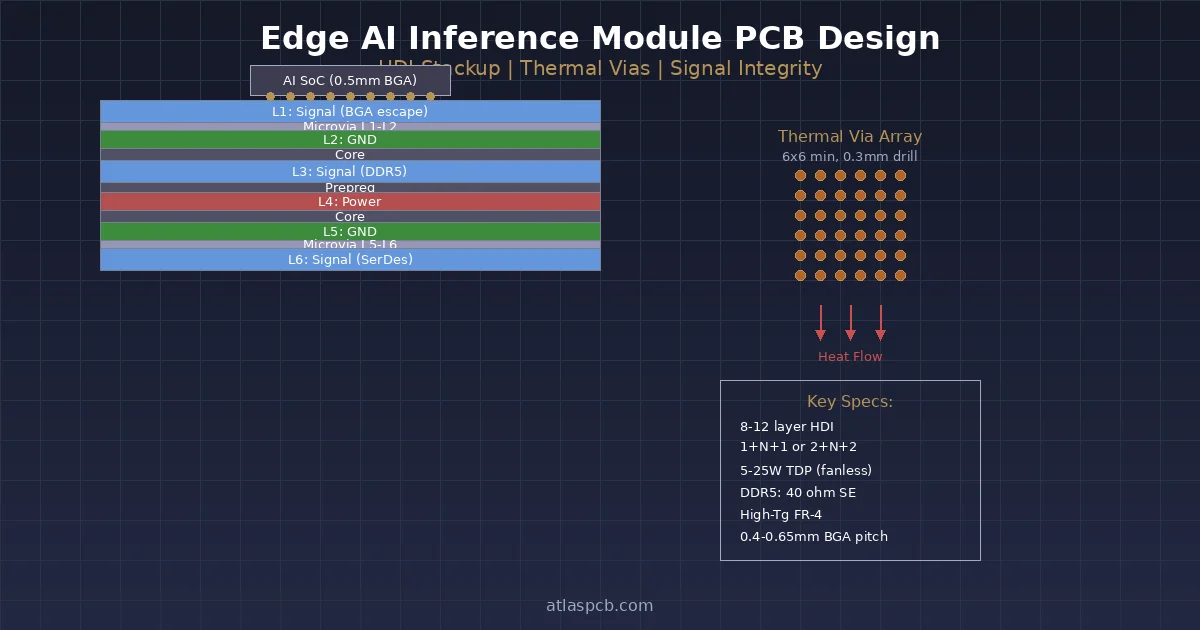
PCB Design for Edge AI Inference Modules: HDI, Thermal, and Signal Integrity
Complete design guide for edge AI inference module PCBs — covering HDI stackup requirements for 0.4-0.65mm BGA escape, thermal via arrays for 5-25W dissipation in compact form factors, DDR4/5 and high-speed SerDes routing, and material selection that balances performance with cost.
Immersion Silver vs ENIG: Which Surface Finish for High-Reliability PCBs?
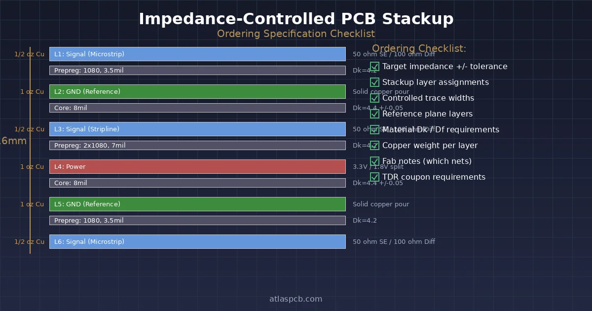
How to Specify Impedance-Controlled PCB Stackup: Complete Ordering Checklist
AI in PCB Manufacturing Goes Mainstream — But Only 10% Have Scaled Deployments
A June 2026 Digitimes report reveals that while AI adoption in PCB manufacturing is now widespread across the industry, fewer than 10% of companies have achieved factory-wide scaled deployments — highlighting the persistent gap between experimentation and production-ready implementation.
AI Accelerator PCB Design: Thermal and Power Delivery Challenges for Next-Gen GPU Modules
Engineering guide for PCB design supporting AI accelerators (GPUs, TPUs, NPUs). Covers thermal via arrays, high-current power delivery networks, and HDI routing for HBM interfaces. Practical design rules for 800W+ AI compute boards.
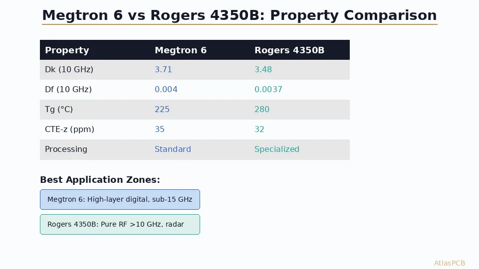
Megtron 6 vs Rogers 4350B: Which High-Frequency Laminate for Your Next Design?
Compare Megtron 6 and Rogers 4350B across Dk, Df, thermal performance, cost, and multilayer compatibility. Engineering decision guide for 5G, radar, and high-speed digital applications.
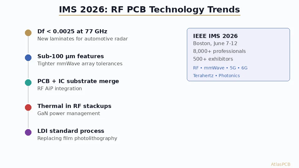
IMS 2026 Boston: RF/Microwave PCB Technology Trends from the Show Floor
Key RF PCB technology developments showcased at IEEE IMS 2026 in Boston (June 7-12). New laminate launches, advanced packaging for mmWave, and what it means for RF board designers ordering in 2026.
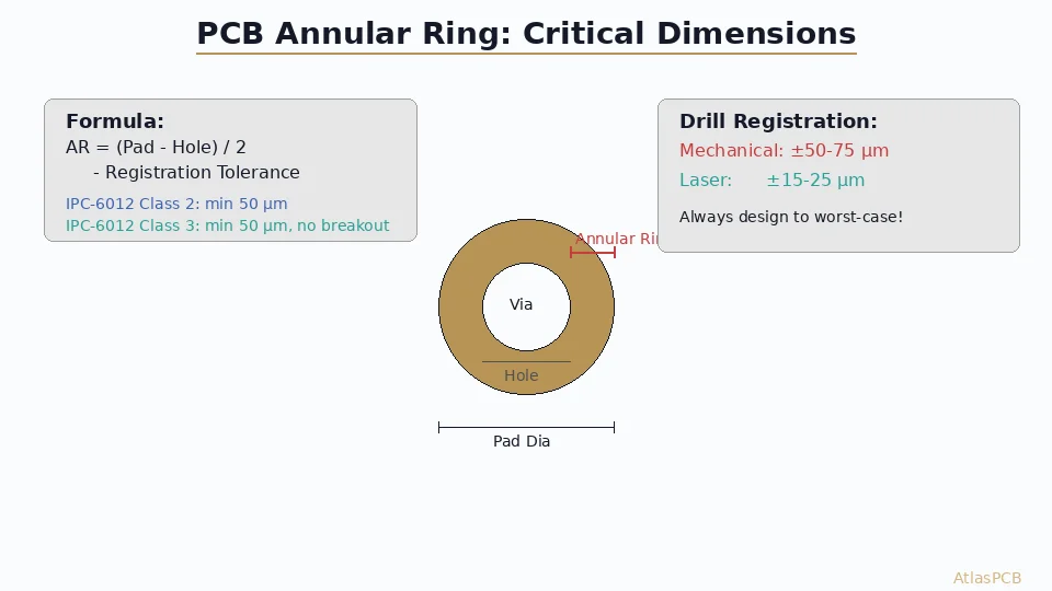
How to Specify Annular Ring Requirements: DFM Guide for Reliable PCB Vias
Complete engineering guide for specifying annular ring width in PCB designs. Covers IPC-6012 Class 2 vs Class 3, minimum values for HDI microvias, and common DFM errors that cause pad breakout.
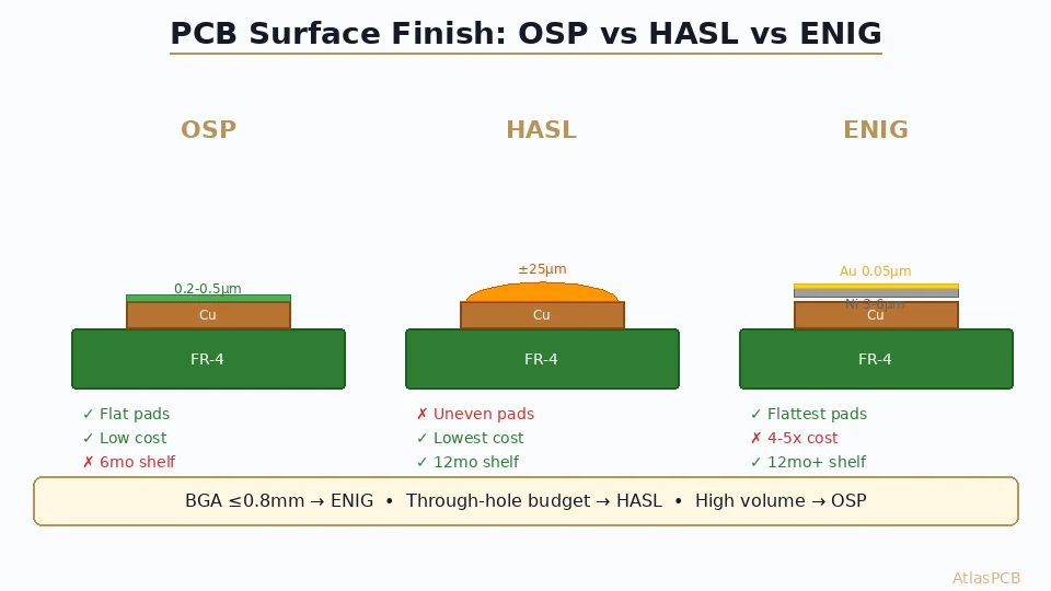
OSP vs HASL vs ENIG: How to Choose the Right PCB Surface Finish (2026 Decision Guide)
Can't decide between OSP, HASL, and ENIG for your PCB? This decision guide gives you the answer in 30 seconds based on your design requirements, budget, and assembly process.
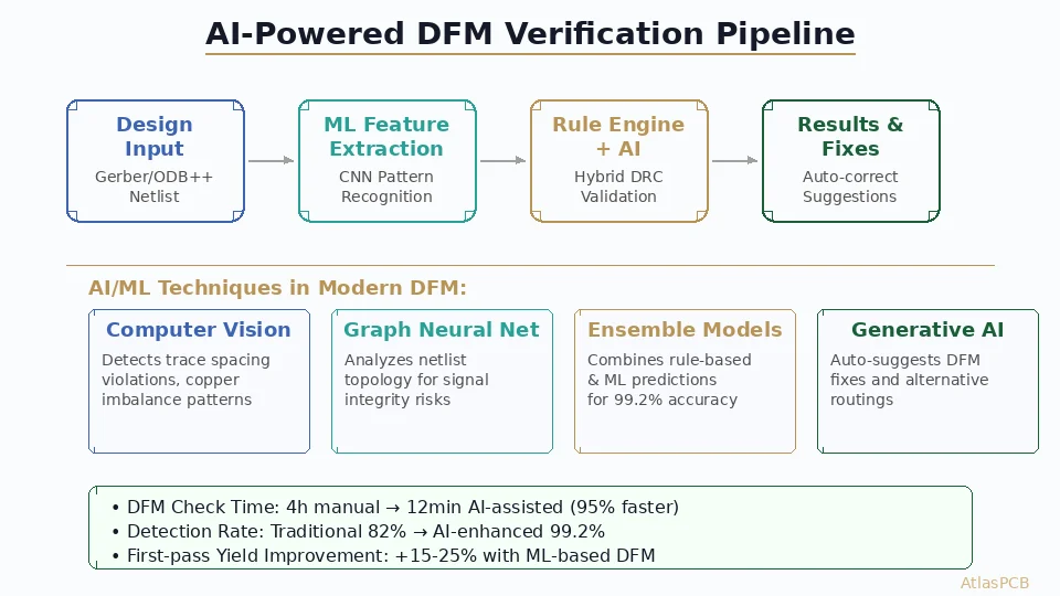
AI-Powered DFM Verification: How Machine Learning Is Automating PCB Design Rule Checking in 2026
Deep dive into how AI and machine learning are transforming PCB Design for Manufacturability verification — from CNN-based pattern recognition detecting acid traps and copper slivers to graph neural networks analyzing netlist topology for signal integrity risks, achieving 99%+ detection rates and 95% faster review cycles versus manual DFM.
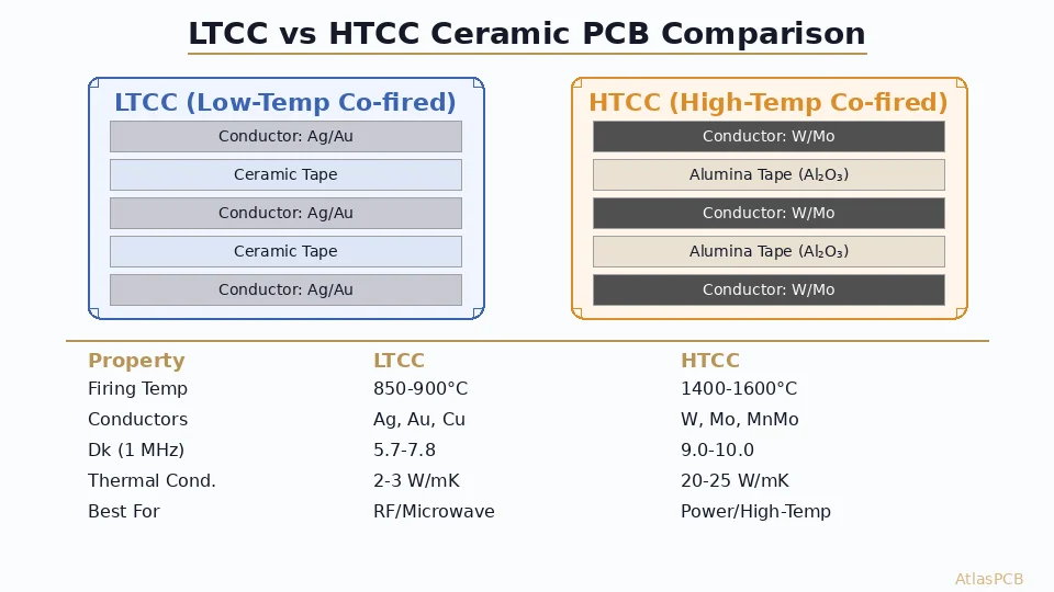
Ceramic PCB Technology: LTCC vs HTCC for High-Temperature and RF Applications
Complete guide to ceramic PCB substrate technology comparing Low-Temperature Co-fired Ceramics (LTCC) and High-Temperature Co-fired Ceramics (HTCC) — covering material properties, firing processes, conductor compatibility, thermal performance, and application selection for RF, aerospace, automotive, and power electronics.
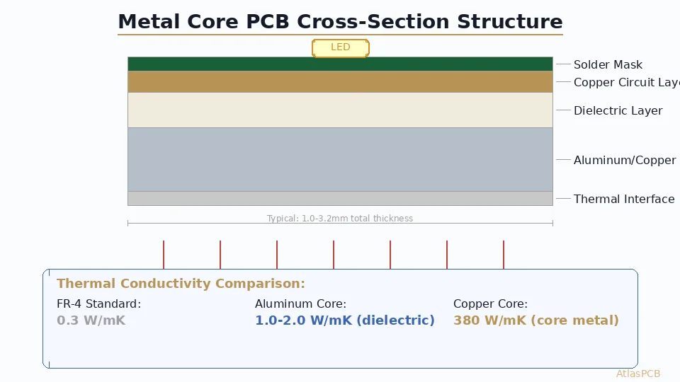
Metal Core PCB (MCPCB) Design Guide: Thermal Management for LED and Power Electronics
Comprehensive design guide for Metal Core PCBs (MCPCBs) covering aluminum and copper core substrates, dielectric layer selection, thermal resistance calculations, single-layer vs multilayer MCPCB architectures, and DFM guidelines for LED lighting, power converters, and motor drive applications.
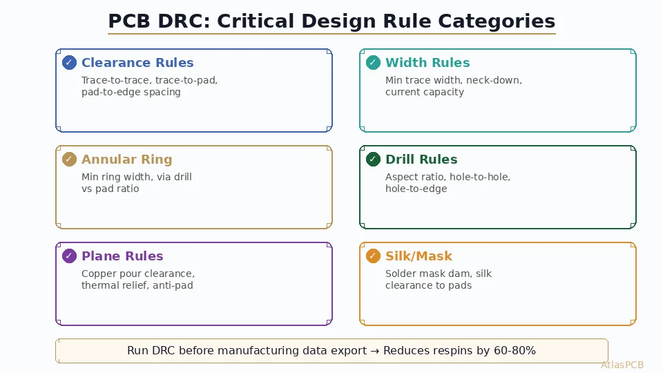
PCB Design Rule Check (DRC): Complete Manufacturability Checklist for Engineers
Definitive PCB DRC guide covering all critical design rule categories — clearance, width, annular ring, drill, plane, solder mask, and silkscreen rules — with specific values for standard, HDI, and advanced manufacturing capabilities, plus common violations and fixes.
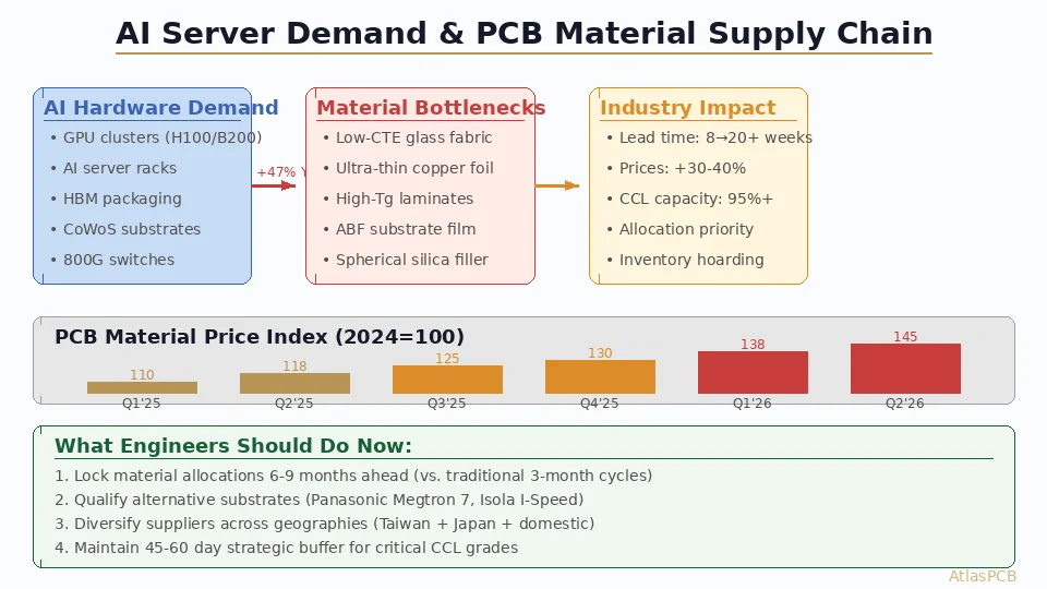
AI Server Demand Is Breaking the PCB Material Supply Chain: What Engineers Must Know About Lead Times, Pricing, and Material Selection in 2026
AI hardware demand has driven PCB raw material prices up 30-40% and lead times from 8 to 20+ weeks. This guide explains the supply chain mechanics, identifies which materials are most constrained, and provides actionable strategies for engineers navigating procurement in 2026.
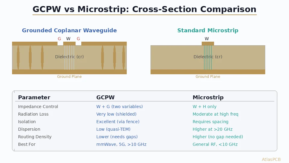
Grounded Coplanar Waveguide (GCPW) PCB Design: When to Choose CPW Over Microstrip for RF Routing
Complete guide to grounded coplanar waveguide (GCPW) design on PCB, covering impedance calculation, gap geometry, via stitching requirements, and comparison with microstrip for mmWave, 5G, and high-frequency applications above 10 GHz.
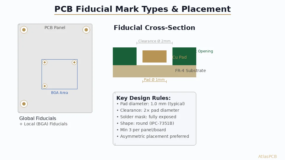
PCB Fiducial Mark Design: Global vs Local Fiducials for Automated Pick-and-Place Assembly
A comprehensive guide to PCB fiducial mark design, covering global and local fiducial placement rules, IPC-7351B requirements, clearance dimensions, and DFA best practices for high-speed automated SMT assembly.
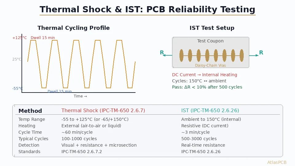
Thermal Shock Testing and IST for PCB Reliability: IPC-TM-650 Methods, Failure Modes, and Pass Criteria
Complete guide to PCB thermal shock testing and Interconnect Stress Testing (IST) per IPC-TM-650 standards. Learn test methods, cycle parameters, failure mechanisms, pass/fail criteria, and when to specify each test for via reliability qualification.
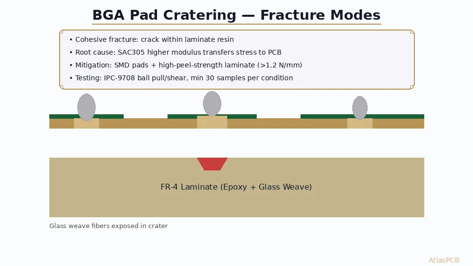
BGA Pad Cratering: Root Causes, IPC-9708 Testing, and PCB Design Mitigations
Complete engineering guide to BGA pad cratering in PCB assemblies. Covers fracture mechanics, IPC-9708 ball pull/shear testing, laminate selection, pad design strategies, and prevention methods for high-reliability electronics.
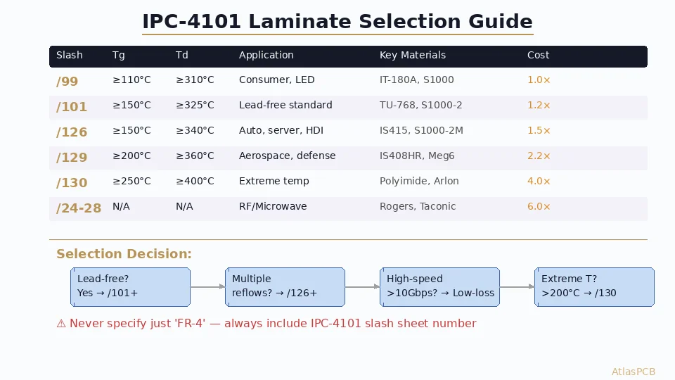
IPC-4101 Laminate Specification Guide: Selecting the Right PCB Base Material
Complete guide to IPC-4101 laminate slash sheets for PCB designers. Covers material classification, key parameters (Tg, Td, Dk, Df, CTE, T-288), and selection criteria for high-speed, high-frequency, automotive, and aerospace applications.
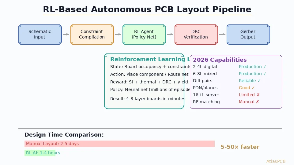
Reinforcement Learning PCB Layout: How Quilter's AI Engine Solves Constraint-Aware Board Generation
Technical deep-dive into reinforcement learning approaches for autonomous PCB layout. Examines Quilter's physics-driven AI engine, constraint compilation, DRC-clean generation, and the implications for hardware design workflows in 2026 and beyond.
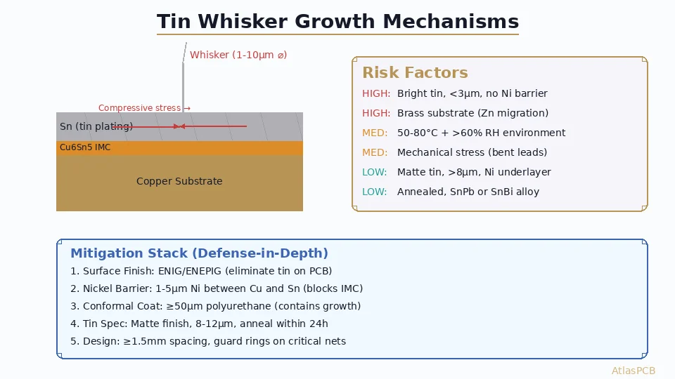
Tin Whisker Growth on PCBs: Risk Assessment, Mechanisms, and Mitigation Strategies
Engineering guide to tin whisker formation on PCB surface finishes and component leads. Covers growth mechanisms, risk factors, JEDEC JEIP39 testing, conformal coating mitigation, and surface finish alternatives for high-reliability electronics.
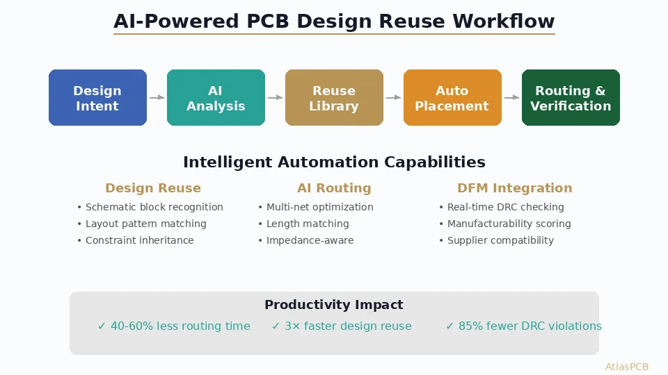
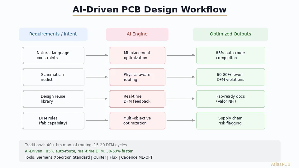
AI-Powered PCB Design Reuse: How Intelligent Automation Is Cutting Layout Time by 60%
Explore how AI-driven design reuse and intelligent automation in EDA tools like Siemens Xpedition are transforming PCB design workflows — reducing routing time, improving DFM compliance, and accelerating time-to-market.
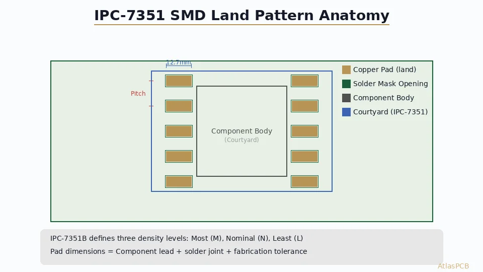
PCB Land Pattern Design: IPC-7351B Footprint Standards for SMD Components
Master IPC-7351B land pattern design for SMD components. Learn density levels, pad dimension calculations, courtyard rules, and thermal relief for optimal PCB assembly yield.
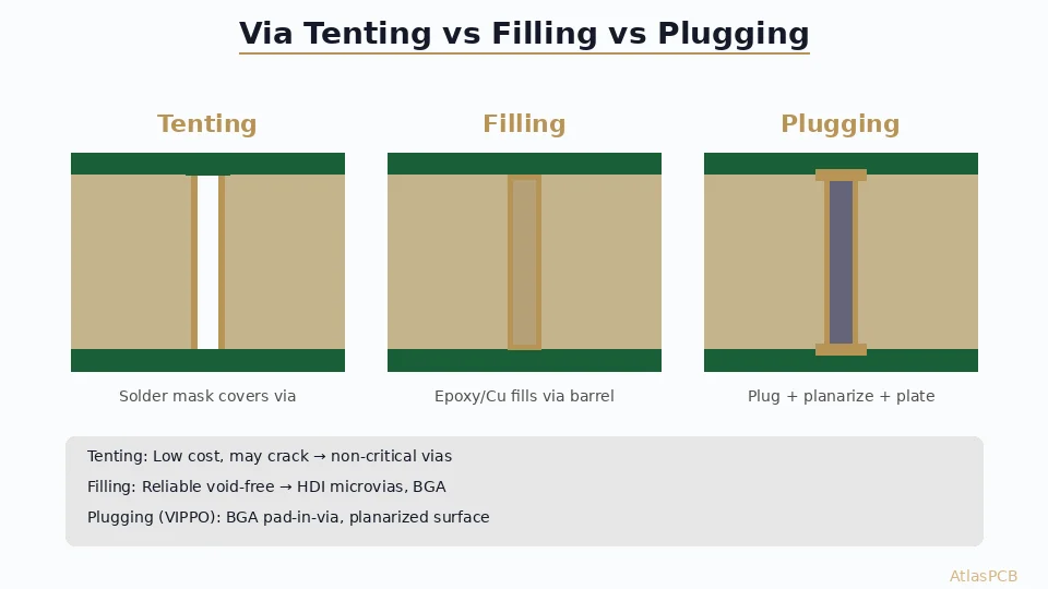
PCB Via Tenting vs Via Filling vs Via Plugging (VIPPO): When to Use Each Method
Complete guide to via protection methods in PCB manufacturing. Compare tenting, conductive/non-conductive filling, and VIPPO plugging for HDI, BGA, and high-reliability designs.
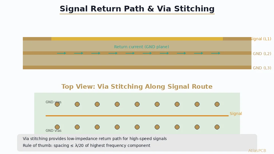
Signal Return Path and Ground Via Stitching in High-Speed PCB Design
Understanding signal return paths and ground via stitching for high-speed PCB design. Learn λ/20 spacing rules, reference plane transitions, and EMI reduction strategies.
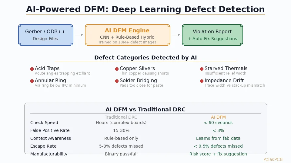
AI-Powered DFM Checking: How Deep Learning Catches PCB Manufacturing Defects Before Fabrication
Explore how AI and deep learning transform PCB design-for-manufacturing (DFM) verification. Learn how CNN-based defect detection, trained on millions of fab images, identifies acid traps, copper slivers, and impedance risks that traditional DRC rules miss.
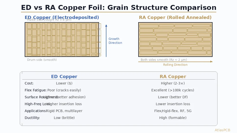
PCB Copper Foil Types: ED vs RA Foil for High-Frequency and Flex Applications
Understand the differences between electrodeposited (ED) and rolled annealed (RA) copper foil for PCB fabrication. Learn how grain structure, surface roughness, and ductility affect signal loss, flex reliability, and manufacturing cost.
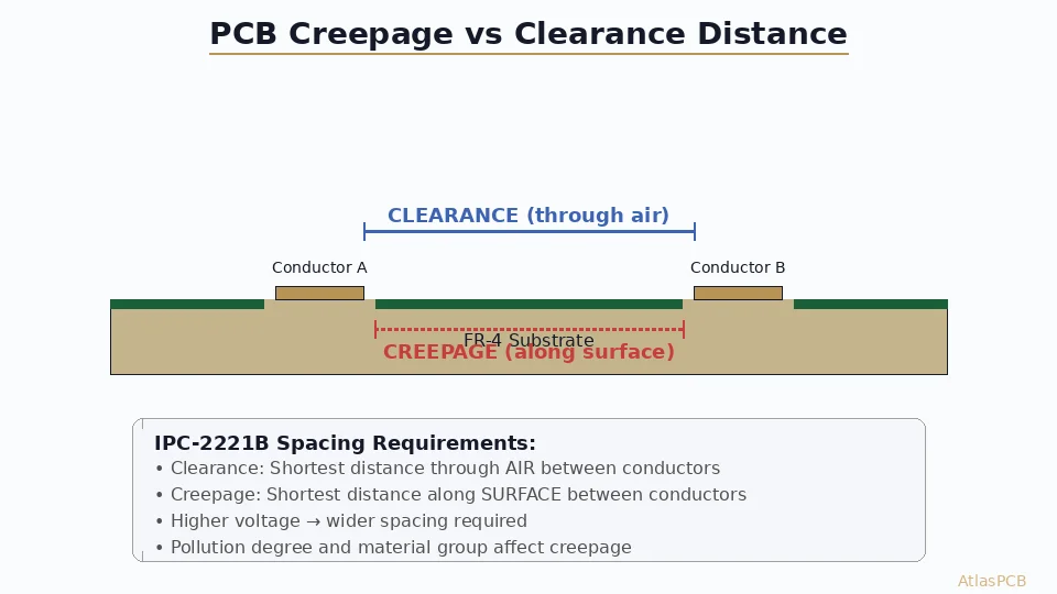
PCB Creepage and Clearance: IPC-2221B High-Voltage Spacing Design Guide
Master IPC-2221B creepage and clearance rules for high-voltage PCB design. Learn how pollution degree, material group, and altitude affect conductor spacing requirements for safe, reliable boards.
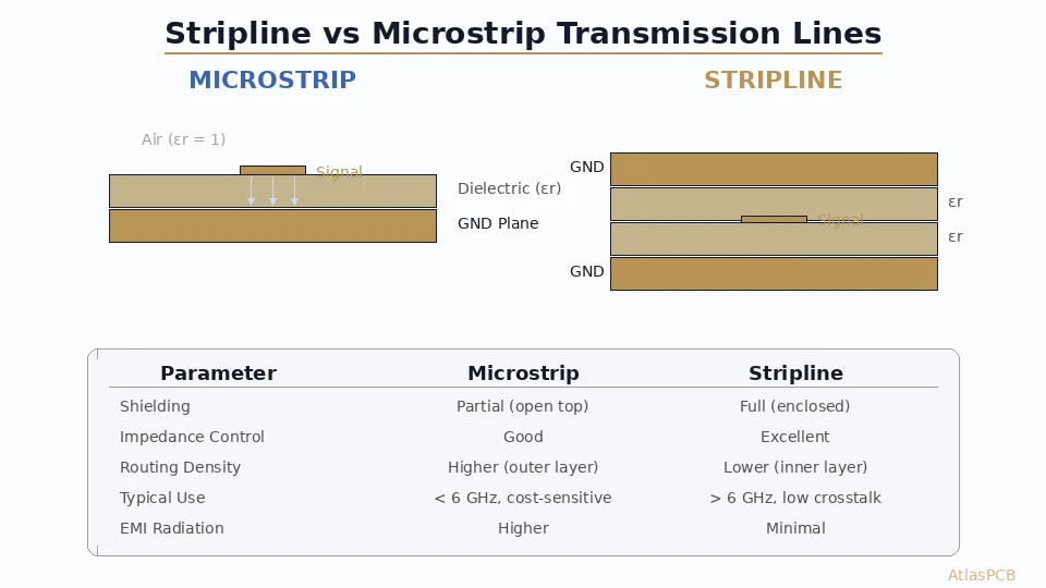
Stripline vs Microstrip: Choosing the Right Transmission Line for PCB Signal Routing
Compare stripline and microstrip transmission line geometries for PCB design. Understand impedance calculations, loss characteristics, EMI behavior, and when to use each topology for optimal signal integrity.
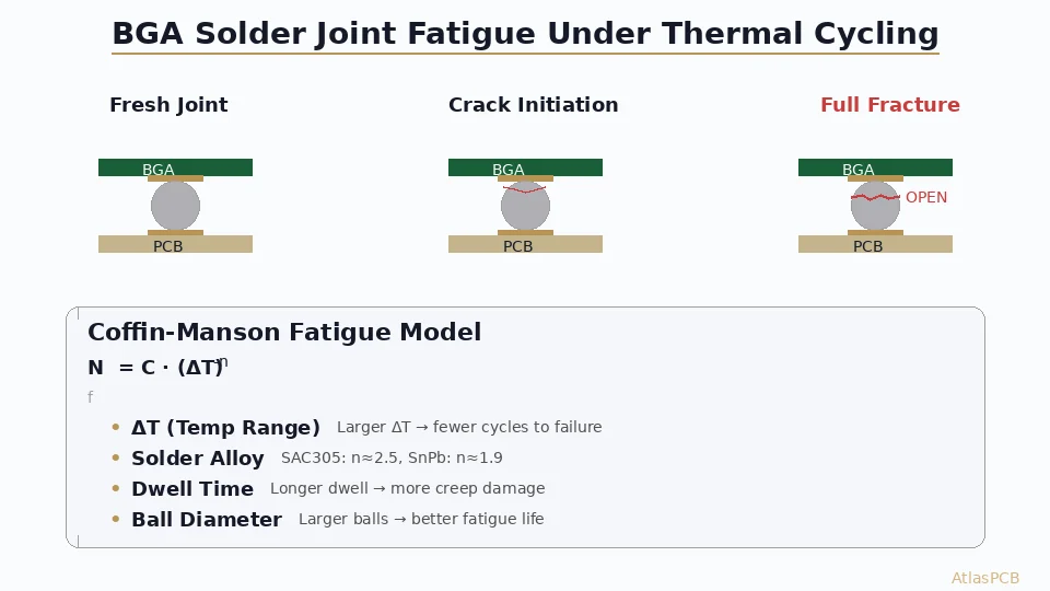
BGA Solder Joint Fatigue: Thermal Cycling Reliability, Coffin-Manson Prediction, and PCB Design Mitigation
Understand how thermal cycling causes BGA solder joint fatigue through creep-fatigue crack propagation. Learn Coffin-Manson lifetime prediction, DNP effects, and PCB design strategies to extend solder joint life.
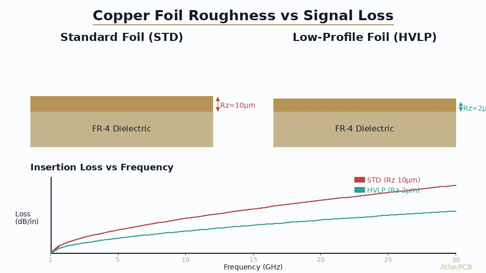
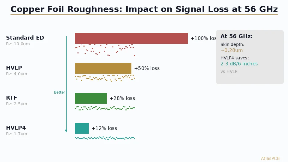
Copper Roughness and High-Speed Signal Loss: How Foil Profile Affects PCB Performance Above 10 GHz
Learn how copper foil surface roughness (Rz) directly increases insertion loss at high frequencies. Compare STD, RTF, HVLP, and ULVP profiles with Huray model predictions for 10–56 Gbps PCB designs.
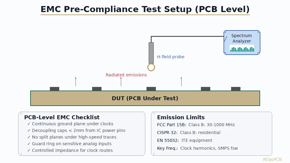
PCB Design for EMC Pre-Compliance: Near-Field Probing, Common-Mode Filtering, and Layout Techniques to Pass FCC/CISPR Tests First Time
Master EMC pre-compliance testing at the PCB level. Learn near-field probing techniques, common-mode noise mitigation, clock routing strategies, and layout best practices that reduce radiated emissions before formal testing.
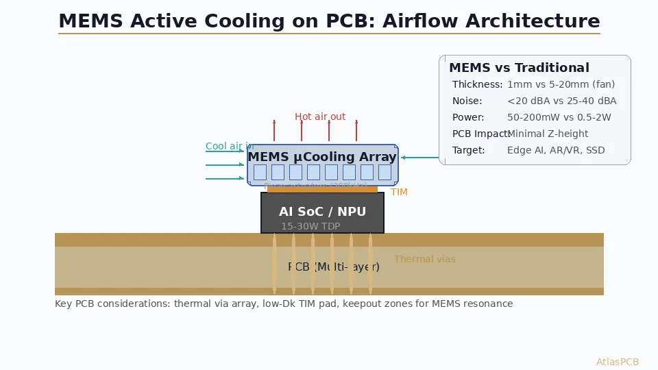
MEMS Active Cooling for Edge AI: How Piezoelectric µCooling Changes PCB Thermal Design
xMEMS and other MEMS cooling startups are bringing sub-1mm active cooling to edge AI devices. Learn how piezoelectric micro-coolers work, their impact on PCB thermal design, and what hardware engineers need to consider for AI glasses, SSDs, and compact NPU boards.
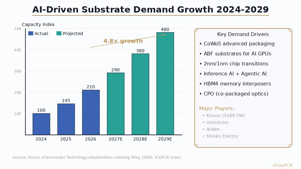
AI-Driven PCB Substrate Demand: How Kinsus Sees Order Visibility Extending to 2029
Taiwanese substrate maker Kinsus reports AI-driven demand for ABF and BT substrates has extended order visibility to 2028-2029, as CoWoS packaging, 2nm chips, and agentic AI drive unprecedented capacity expansion. Analysis of what this means for PCB manufacturers and hardware engineers.
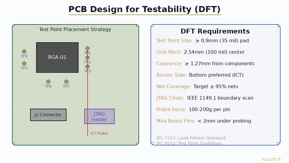
PCB Design for Testability (DFT): Test Point Placement, ICT Access, and Boundary Scan Strategy
Complete guide to PCB design for testability. Learn IPC-9252 test point requirements, bed-of-nails fixture access rules, flying probe accommodation, JTAG boundary scan integration, and how DFT reduces manufacturing defect escape rates below 10 ppm.
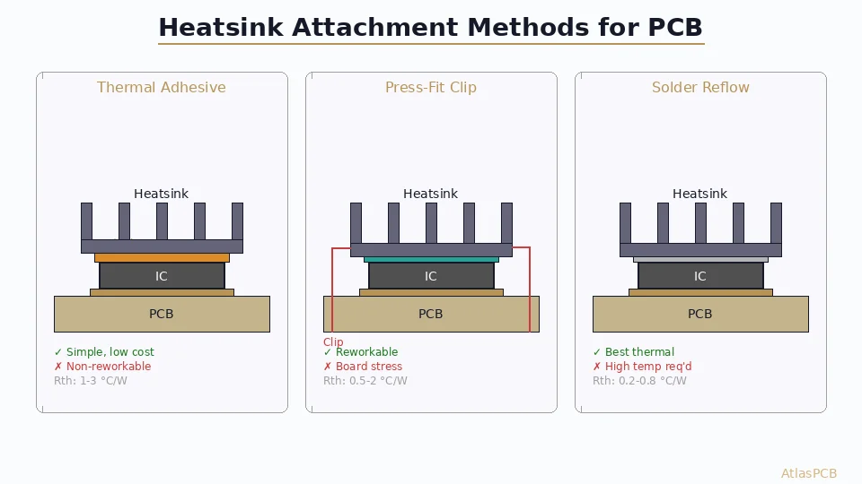
PCB Heatsink Attachment Methods: Thermal Adhesive, Mechanical Clip, and Solder Reflow Mounting
Compare PCB heatsink attachment methods including thermal adhesive, spring-clip mechanical mounting, and solder-reflow bonding. Learn thermal resistance values, rework considerations, and design rules for each approach to optimize power dissipation in high-current PCB assemblies.
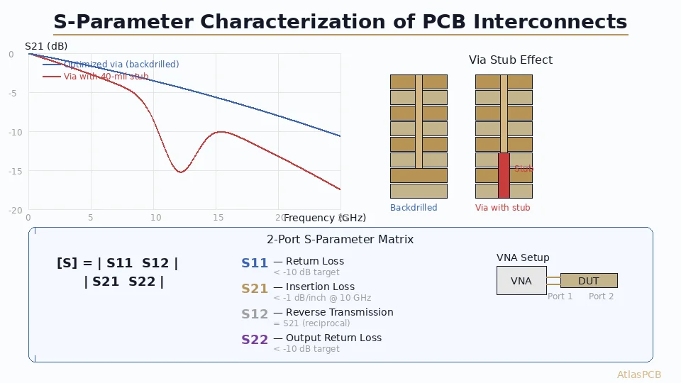
S-Parameter Characterization of PCB Interconnects: Via Transitions, Connectors, and Transmission Lines
Master S-parameter measurement and modeling for PCB interconnects. Learn how to extract insertion loss (S21), return loss (S11), and crosstalk from via transitions, connectors, and differential pairs using VNA measurements and 3D EM simulation — essential for 25+ Gbps SerDes channel design.
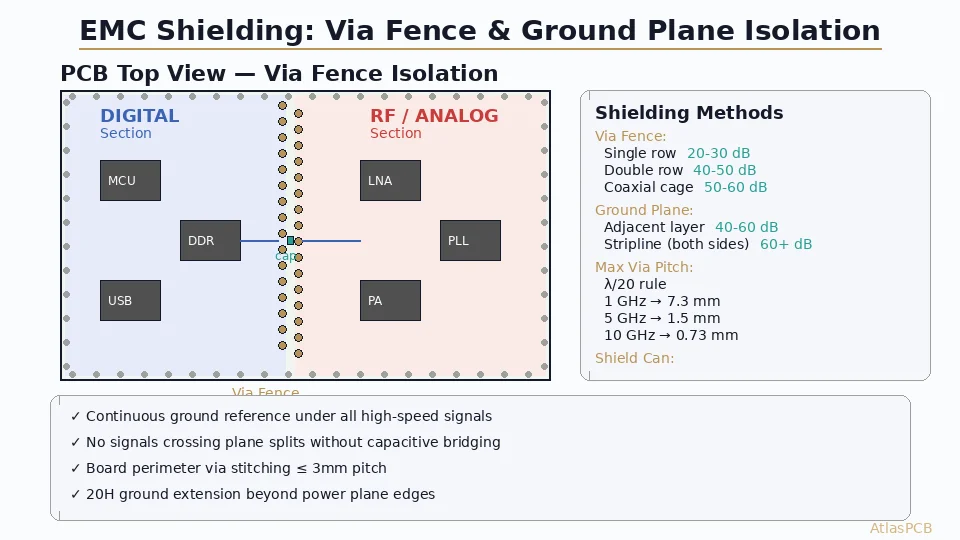
EMC Shielding Techniques in PCB Layout: Ground Planes, Via Fencing, and Guard Traces
Comprehensive guide to PCB-level EMC shielding. Covers ground plane design, via stitching fences, guard traces, split plane management, and shield can integration for passing radiated emissions tests.
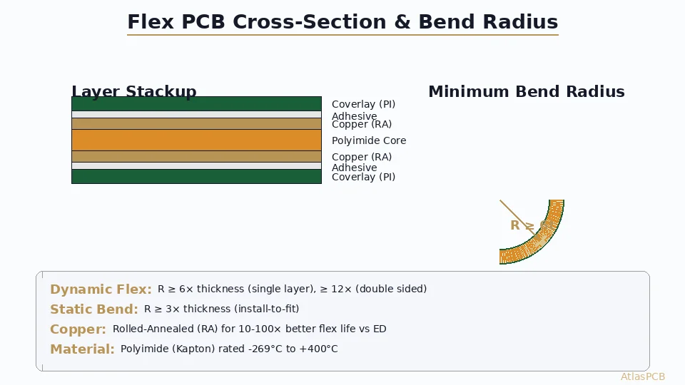
Flex and Rigid-Flex PCB Design Guidelines: Bend Radius, Stackup, and Reliability
Master flex and rigid-flex PCB design with proven guidelines for bend radius calculations, stackup planning, material selection, and reliability testing. Covers IPC-2223 standards and manufacturing best practices.
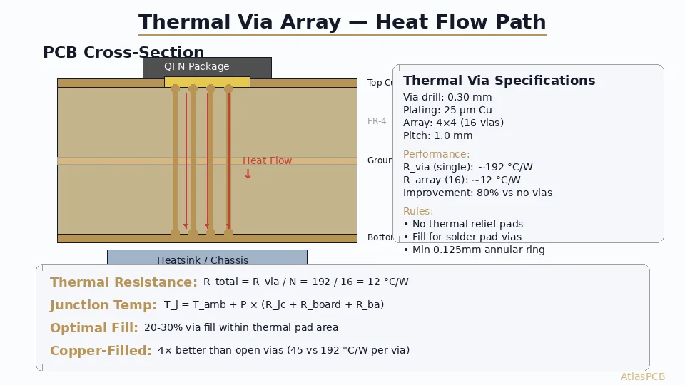
Thermal Via Design for PCB Heat Dissipation: Array Patterns, Copper Fill, and Simulation
Complete guide to thermal via design in PCBs. Covers via array calculations, copper fill percentages, thermal resistance modeling, and design rules for power components, LEDs, and RF amplifiers.
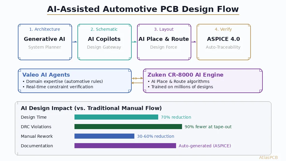
Valeo and Zuken Launch AI-Assisted Automotive PCB Design Platform: What It Means for EDA
Valeo and Zuken's 'InnoLab' partnership combines AI agents with Design Force PCB tools — automating architecture generation, schematic entry, and auto-placement for ASPICE 4.0 compliant automotive electronics.
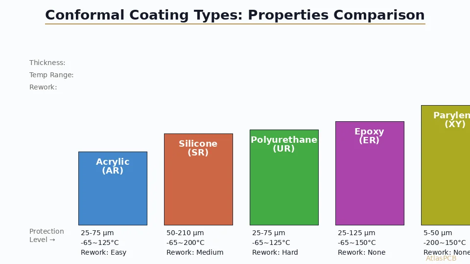
Conformal Coating for PCBs: Types, Application Methods, and IPC-CC-830 Compliance
Complete guide to PCB conformal coating materials (acrylic, silicone, polyurethane, parylene, epoxy), application methods (spray, dip, selective), thickness requirements, and IPC-CC-830 qualification testing for harsh environment protection.
Heavy Copper PCB Design for Power Electronics: Bus Bars, Current Capacity, and Thermal Management
Learn how heavy copper PCBs (3-20 oz) enable reliable power electronics design. Covers current capacity calculations, bus bar integration, thermal management strategies, and manufacturing considerations for high-current applications.
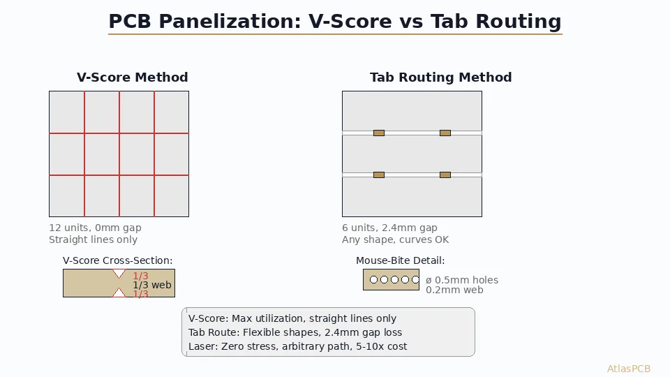
PCB Panelization and Depaneling: V-Score, Tab Routing, and Laser Singulation Methods
Master PCB panelization design with v-scoring, tab routing, and laser depaneling. Learn panel array optimization, breakaway tab design rules, stress-free singulation for sensitive assemblies, and cost-per-unit panel efficiency calculations.
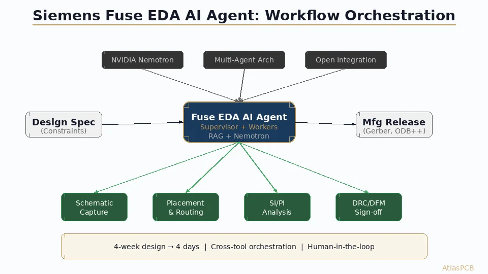
Siemens Fuse EDA AI Agent: How Autonomous Workflow Orchestration Is Changing PCB Design in 2026
Siemens' new Fuse EDA AI Agent brings autonomous multi-tool orchestration to PCB and semiconductor design. Explore how agentic AI with RAG, NVIDIA Nemotron, and physics-aware planning automates end-to-end EDA workflows — from schematic capture to manufacturing sign-off.
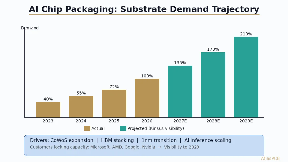
AI-Driven Substrate Demand: How AI Chips Are Extending PCB Order Visibility to 2029
Kinsus Interconnect reports AI-driven substrate orders now extend visibility into 2028-2029. Analyze how CoWoS packaging expansion, HBM stacking, and the 1nm process transition are reshaping PCB substrate capacity planning and what this means for the broader supply chain.
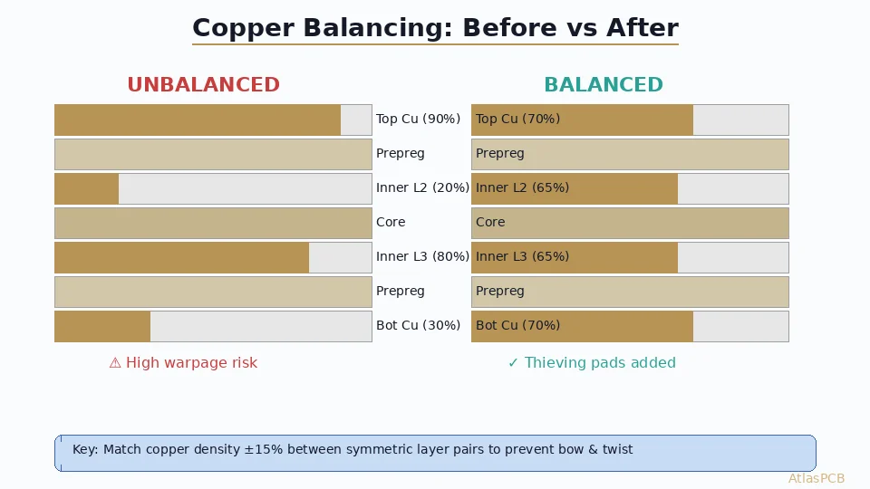
Copper Balancing and Thieving for PCB: Preventing Warpage in Multilayer Boards
Learn how copper balancing and thieving patterns prevent bow and twist in multilayer PCBs. Covers design rules, IPC-2221 guidelines, DFM copper distribution, and practical CAD implementation for 4-layer to 20+ layer stackups.
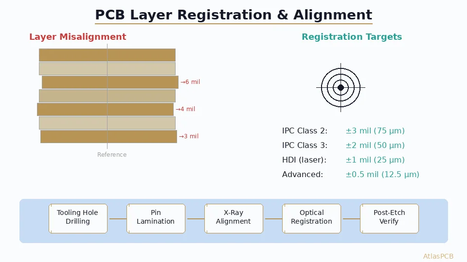
PCB Layer-to-Layer Registration: Alignment Accuracy, Tolerances, and Manufacturing Methods
Complete guide to PCB layer-to-layer registration accuracy. Covers IPC Class 2 and Class 3 alignment tolerances, pin lamination vs mass lamination, X-ray registration systems, and design rules for achieving ±1 mil accuracy in HDI multilayer boards.
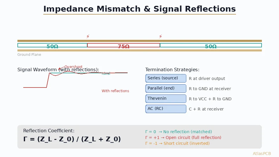
Signal Reflections and Impedance Mismatch on PCBs: Termination Strategies for High-Speed Design
Understand how impedance discontinuities cause signal reflections, ringing, and overshoot on PCB transmission lines. Learn series, parallel, Thevenin, and AC termination techniques with design equations and practical layout guidelines for multi-gigabit interfaces.
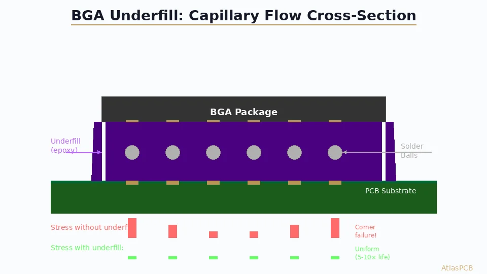
BGA Underfill for PCB Assembly: Capillary, Molded and Reworkable Materials Selection Guide
Complete guide to BGA underfill selection for high-reliability PCB assemblies. Compare capillary flow, molded underfill, and reworkable formulations — with process parameters, CTE matching, and reliability data for automotive and aerospace applications.
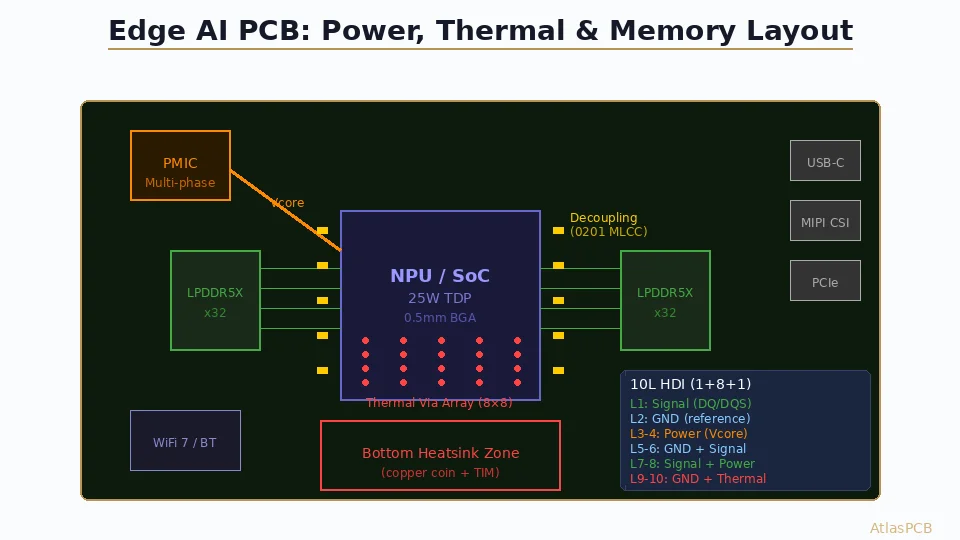
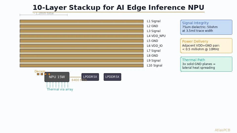
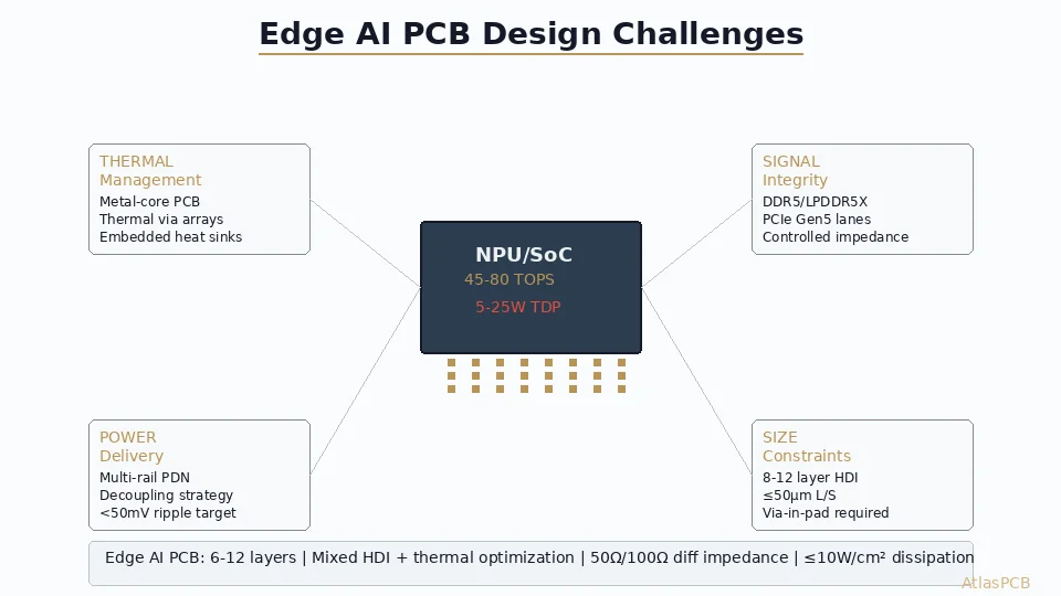
Edge AI PCB Design in 2026: Power Delivery, Thermal Management and High-Speed Layout for On-Device Inference
The inference flip is here — two-thirds of AI compute now runs at the edge. Learn how to design PCBs for edge AI processors including NPU power delivery networks, thermal via arrays, LPDDR5X routing, and HDI stackup strategies that ship reliable products.
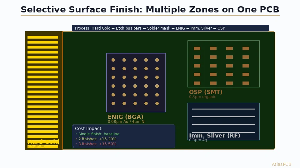
Selective Surface Finish on PCB: Combining ENIG, OSP, Hard Gold and Immersion Silver on One Board
Learn how to specify multiple surface finishes on a single PCB for optimal cost and performance. Covers process sequencing, masking techniques, DFM rules, and real-world applications in connector, RF, and mixed-technology designs.
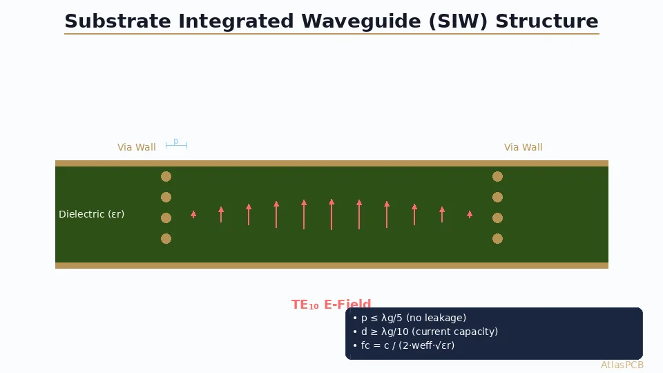
Substrate Integrated Waveguide (SIW) PCB Design: Filters, Couplers and Antennas for mmWave Applications
Master SIW design on standard PCB substrates. Learn via fence rules, cutoff frequency calculations, transition design from microstrip to SIW, and practical fabrication guidelines for 24–77 GHz applications.
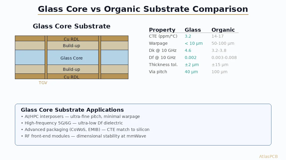
Glass Core Substrates for Advanced PCB Packaging: Technology, Benefits, and Manufacturing Challenges
Explore how glass core substrates are transforming advanced packaging with ultra-low warpage, fine-pitch TGV interconnects, and superior dimensional stability for AI/HPC and RF applications.
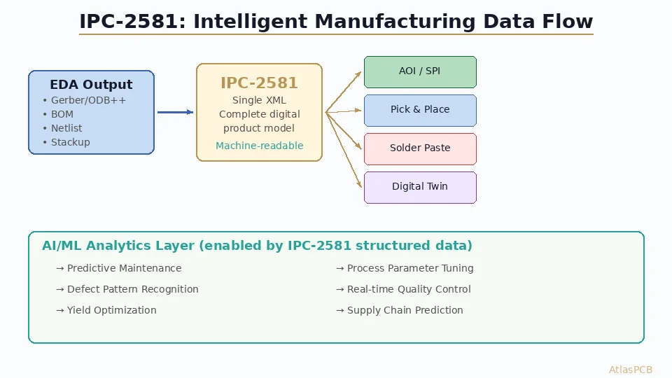
IPC-2581 for Smart Factory PCB Manufacturing: Machine-Readable Data and AI-Ready Production
How IPC-2581 intelligent manufacturing data standard enables AI-driven automation, digital twins, and predictive quality control in modern PCB fabrication and assembly.
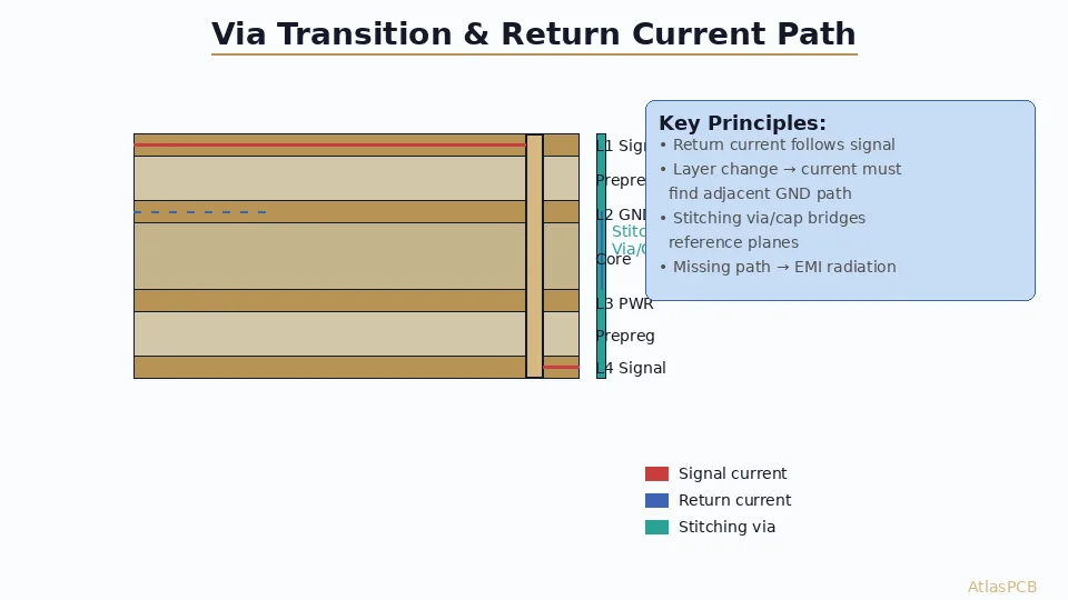
PCB Via Transitions and Return Current Paths: A Signal Integrity Design Guide
Master via transitions in multi-layer PCBs by understanding return current behavior, reference plane changes, and stitching via placement to minimize EMI and preserve signal quality.
Quilter AI Proves Autonomous PCB Layout Works: Project Speedrun Delivers a Working Single-Board Computer
How Quilter.ai's Project Speedrun validated AI-powered PCB layout by autonomously placing and routing a complete NXP i.MX 8M Mini SBC with LPDDR4 — demonstrating production-ready AI layout for real hardware.
AI-Powered DFM Checking for PCB Design: How Machine Learning Replaces Rule-Based Verification
How AI and machine learning are transforming PCB design-for-manufacturing checks — from static rule engines to intelligent systems that learn defect patterns, predict yield issues, and auto-suggest design fixes.
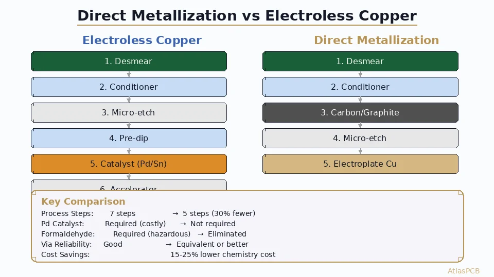
Direct Metallization for PCB Manufacturing: Carbon, Graphite, and Conductive Polymer Processes Explained
A comprehensive guide to direct metallization technologies that replace electroless copper in PCB via formation — comparing carbon, graphite, and conductive polymer methods for HDI production.
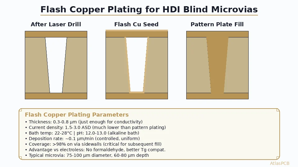
Flash Copper Plating for HDI Microvias: Achieving Uniform Seed Layers in mSAP Process
Technical deep-dive into flash copper plating technology for HDI blind microvias — process parameters, seed layer uniformity, and advantages over electroless copper for mSAP and advanced substrate fabrication.
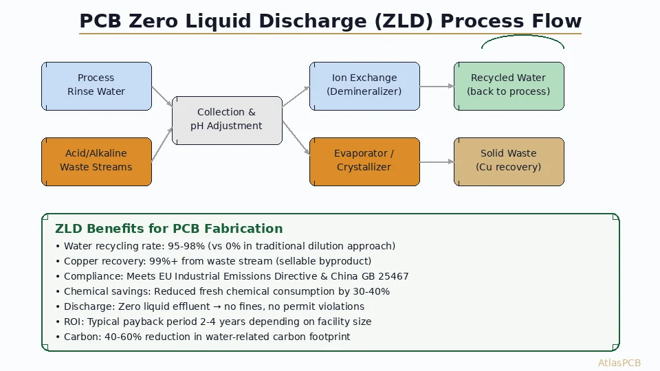
Zero Liquid Discharge in PCB Manufacturing: Wastewater Treatment, Copper Recovery, and Sustainability
How modern PCB fabricators achieve zero liquid discharge through ion exchange, evaporation, and crystallization — eliminating wastewater while recovering valuable metals.
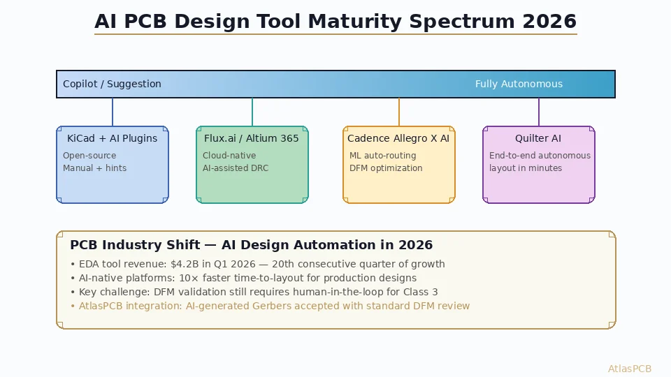
AI PCB Design Tools in 2026: From Copilot Assistants to Fully Autonomous Layout Engines
Explore the 2026 landscape of AI-powered PCB design tools — from KiCad AI plugins and Flux.ai cloud copilots to Quilter's end-to-end autonomous layout. Learn how AI is reshaping EDA workflows and what it means for PCB manufacturing.
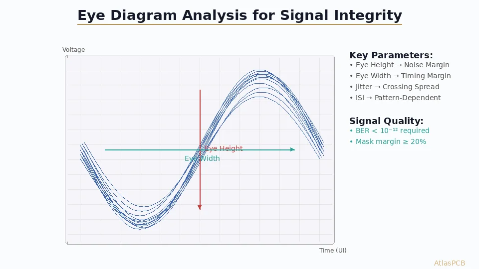
Eye Diagram Interpretation for PCB Signal Integrity: Jitter, ISI and Channel Loss Analysis
Learn to interpret eye diagrams for high-speed PCB signal integrity — understand eye height, eye width, jitter components, inter-symbol interference (ISI), and how PCB design choices affect 10-56 Gbps channel performance.
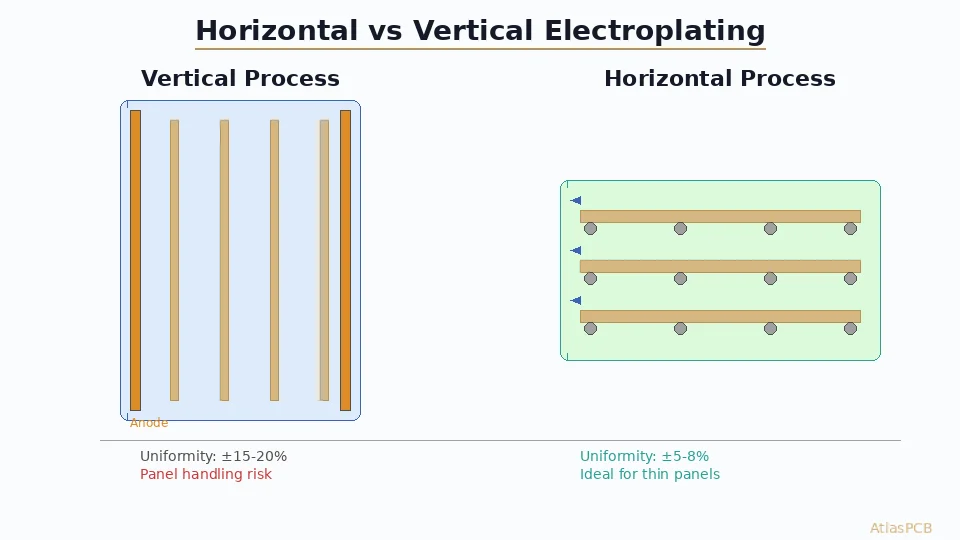
Horizontal vs Vertical Electroplating for PCB: Uniformity, Throughput and HDI Capability
Compare horizontal and vertical electroplating processes for PCB manufacturing — understand how each method affects copper thickness uniformity, production throughput, thin-panel handling, and suitability for HDI and advanced substrates.
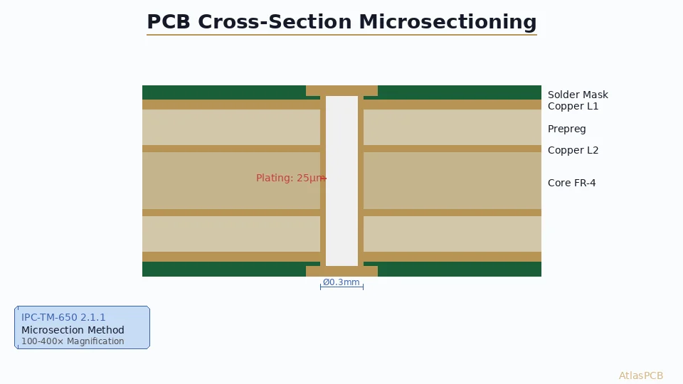
PCB Microsectioning and Cross-Section Analysis: IPC-TM-650 Methods for Via Plating and Registration Inspection
Master PCB microsectioning techniques per IPC-TM-650 2.1.1 — learn sample preparation, polishing procedures, and measurement protocols to verify plating thickness, via quality, and inner-layer registration in production boards.
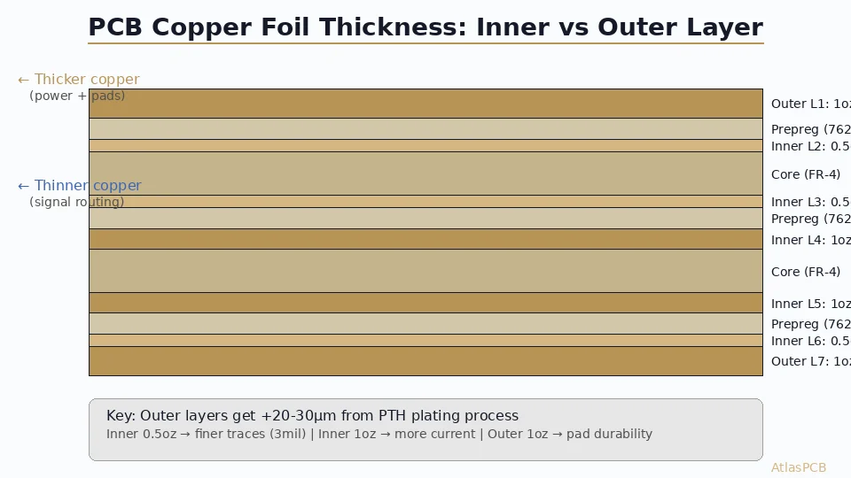
PCB Copper Foil Thickness Selection: Inner Layer vs Outer Layer Design Rules
Master copper foil thickness selection for multilayer PCBs. Compare standard 1oz vs heavy 2oz+ copper, understand inner layer vs outer layer considerations, calculate current capacity, and optimize stackup design for impedance control and thermal management.
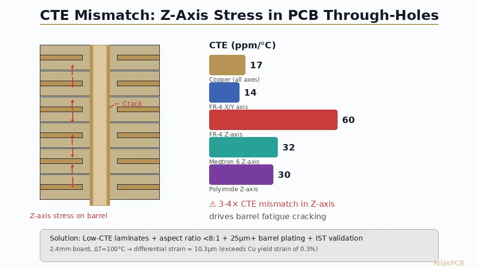
PCB CTE Mismatch and Thermal Stress: Prevention Strategies for Multilayer Board Reliability
Understand how coefficient of thermal expansion (CTE) mismatch causes PCB failures. Learn to calculate z-axis stress, select compatible materials, design via structures for thermal cycling survival, and validate reliability through IST and thermal shock testing.
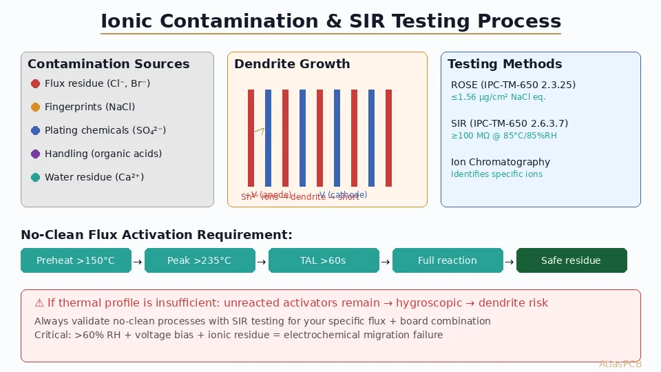
Ionic Contamination Testing for PCB Assembly: No-Clean Flux Residue, SIR, and IPC-J-STD-001 Compliance
Complete guide to ionic contamination control in PCB assembly. Covers ROSE testing, SIR (Surface Insulation Resistance), ion chromatography, no-clean flux residue behavior, IPC cleanliness standards, and practical contamination prevention strategies for high-reliability electronics.
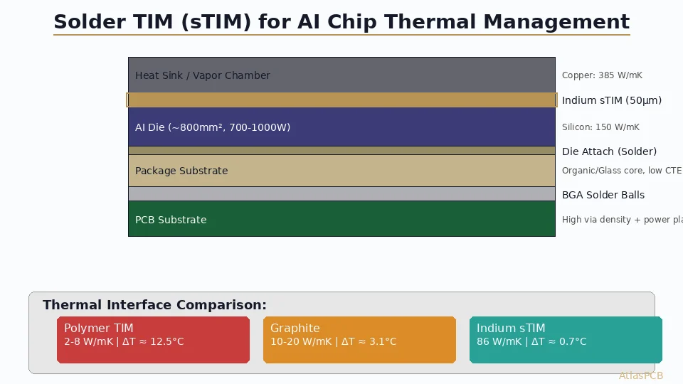
Solder Thermal Interface Materials (sTIMs) for AI Chip Packaging: Indium-Based Solutions at ECTC 2026
Explore how indium-based solder thermal interface materials (sTIMs) with 86 W/mK conductivity are solving AI processor thermal challenges. Learn about vacuum formic acid reflow, voiding minimization, and how PCB substrate design must evolve to support next-generation thermal solutions for data center AI accelerators.
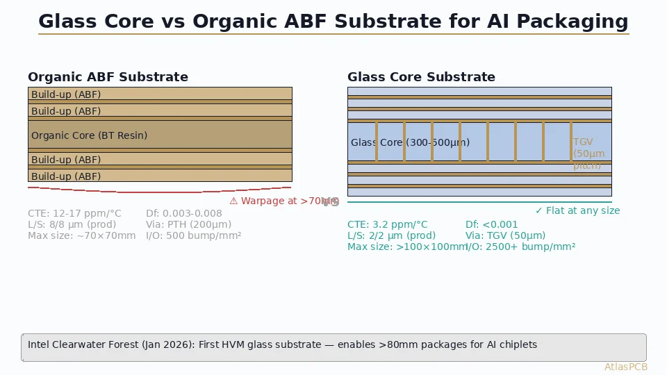
Glass Core Substrates for AI Packaging: How Intel's Clearwater Forest Changes the PCB Substrate Roadmap
Intel's high-volume glass substrate manufacturing for Xeon 6+ processors signals a paradigm shift from organic ABF substrates. Understand the implications for PCB fabricators, material suppliers, and AI hardware designers.
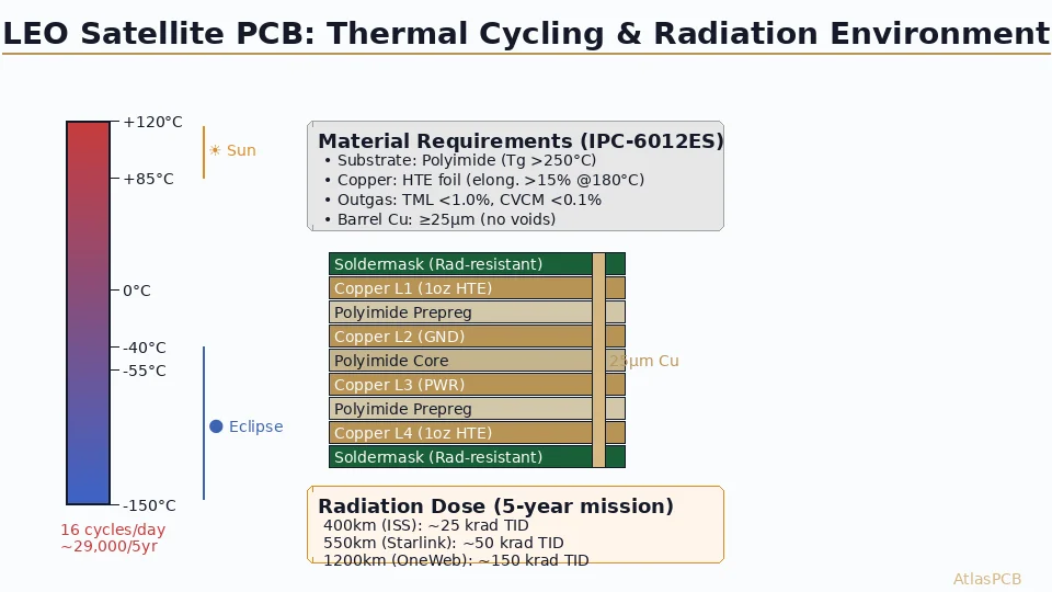
PCB Design for LEO Satellites: Radiation Hardening, Thermal Cycling, and Outgassing Requirements
Design PCBs that survive low-Earth orbit. Covers radiation-tolerant material selection, thermal cycling from -150°C to +120°C, outgassing per NASA ASTM E595, and vibration qualification for satellite and constellation hardware.
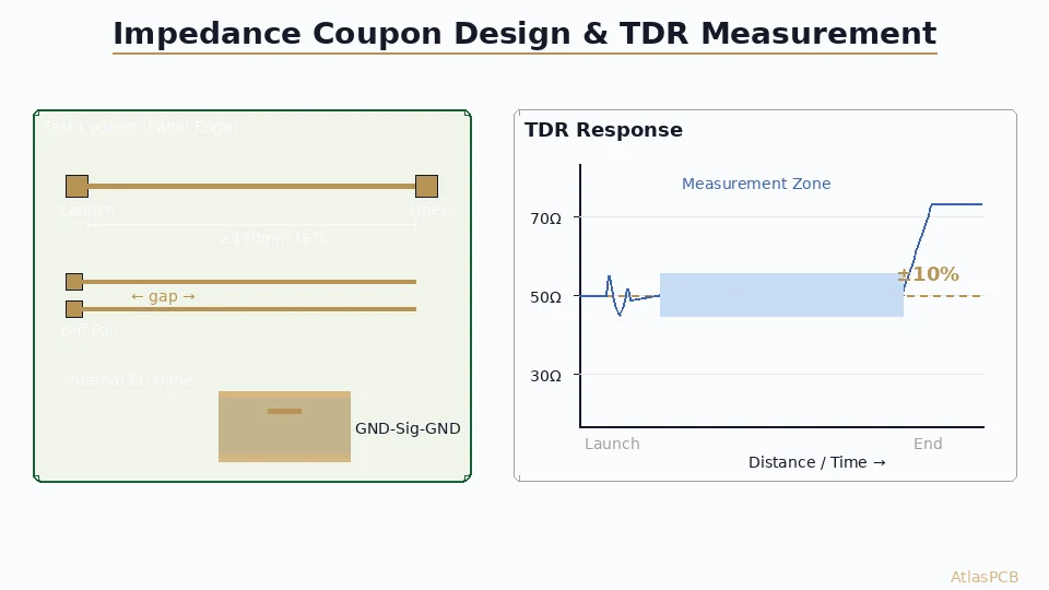
PCB Impedance Coupon Design and TDR Testing: Engineer's Validation Guide
Learn how to design impedance test coupons, interpret TDR results, and specify controlled impedance PCBs. Covers IPC-2141A coupon types, stripline vs microstrip validation, and common impedance failure root causes.
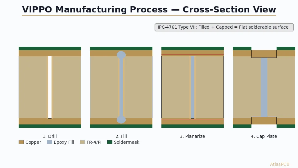
VIPPO (Via-in-Pad Plated Over): Complete PCB Design and Manufacturing Guide
Master VIPPO technology for BGA breakout, fine-pitch components, and high-density PCB designs. Learn IPC-4761 types, manufacturing process steps, design rules, and cost optimization strategies.
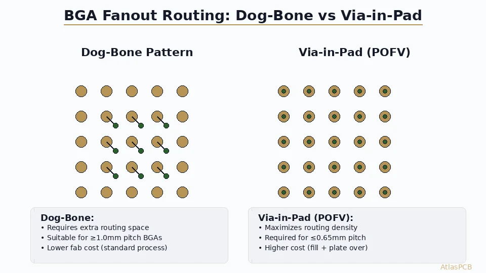
BGA Fanout Routing Strategies: Dog-Bone vs Via-in-Pad Breakout for Fine-Pitch Packages
Master BGA fanout routing with detailed strategies for dog-bone and via-in-pad breakout patterns. Covers 0.4mm to 1.27mm pitch BGAs with layer assignment, escape routing, and DFM considerations.
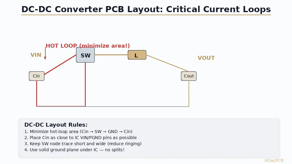
DC-DC Converter PCB Layout: Hot Loop Optimization and EMI Reduction Techniques
Learn critical PCB layout techniques for DC-DC buck and boost converters. Covers hot loop minimization, component placement, ground plane strategies, and thermal management for switching regulators from 100kHz to 5MHz.
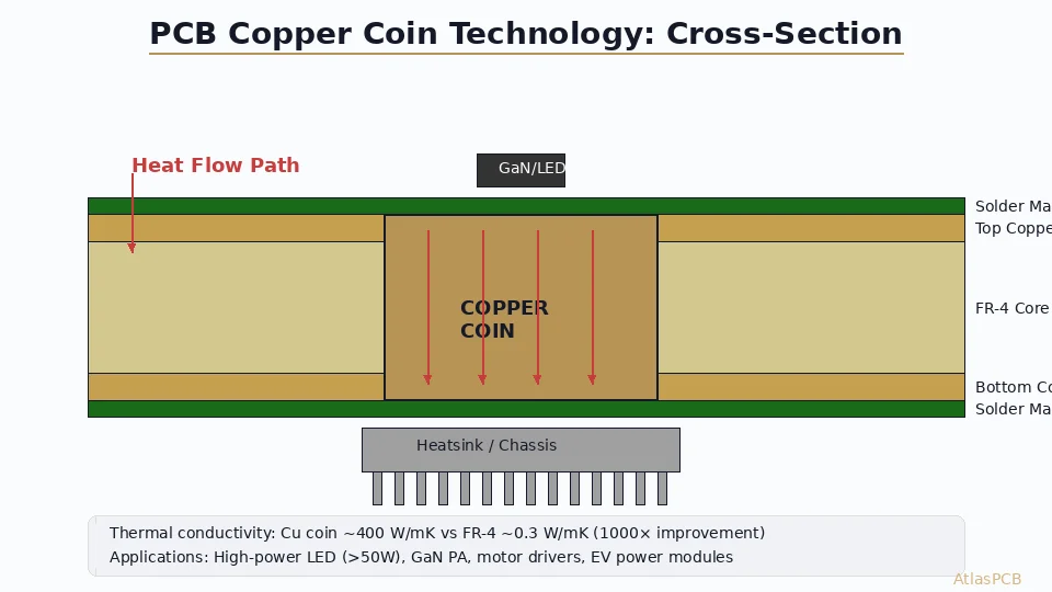
PCB Copper Coin Technology: Embedded Thermal Solutions for High-Power Applications
Complete engineering guide to PCB copper coin (embedded copper slug) technology for thermal management in high-power LEDs, GaN PAs, motor drivers, and EV power modules. Covers design rules, manufacturing process, and thermal performance comparison.
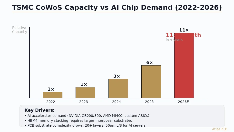
TSMC CoWoS 11× Capacity Growth: How AI Packaging Demand Is Reshaping PCB Substrate Technology
Deep analysis of TSMC's 11× CoWoS capacity expansion and its cascading impact on PCB substrate technology—from ABF substrate shortages to glass-core innovations, 50μm design rules, and the convergence of IC packaging with PCB fabrication.
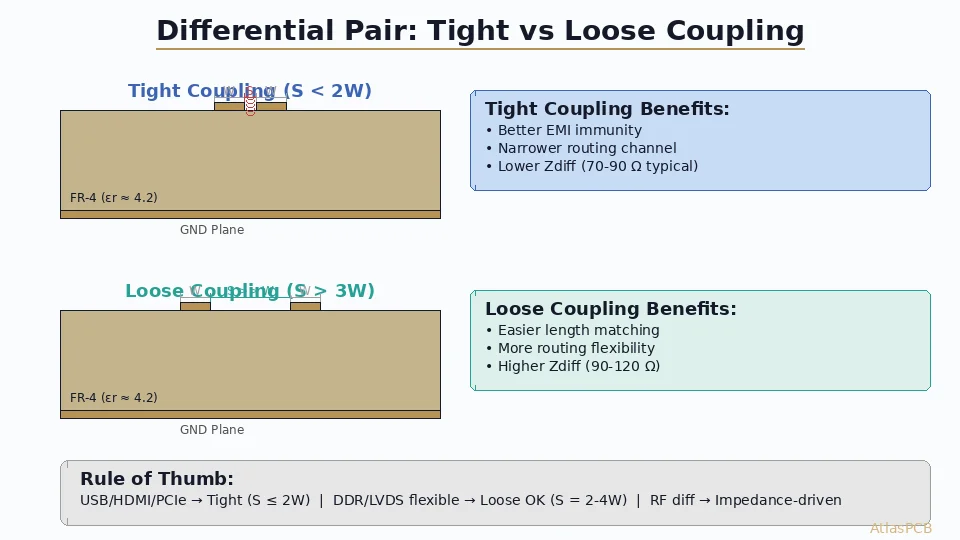
Differential Pair Routing: Tight vs Loose Coupling Strategy for High-Speed PCB Design
Master differential pair routing with this engineering guide on tight vs loose coupling. Learn when to use each approach for USB, PCIe, DDR5, HDMI, and RF applications with impedance calculations and layout examples.
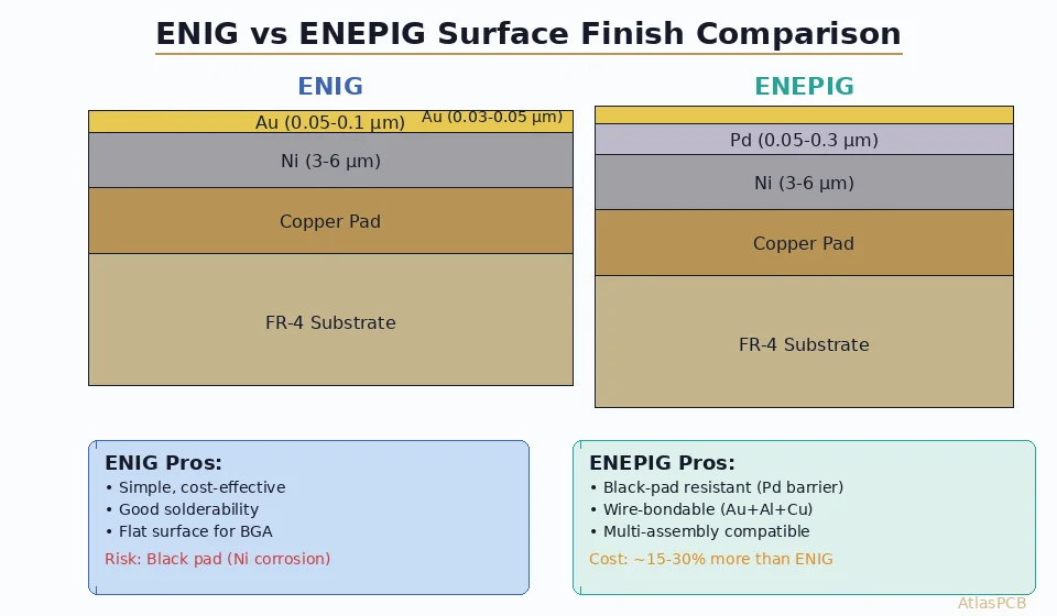
ENIG vs ENEPIG Surface Finish: Complete Selection Guide for PCB Assembly
Learn when to choose ENIG or ENEPIG surface finish for your PCB. Compare cost, reliability, wire bonding compatibility, and black pad risk. Engineering decision framework included.
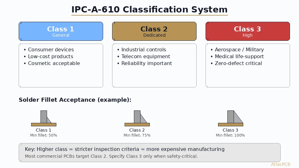
IPC-A-610 Acceptance Criteria: Complete Guide to Electronic Assembly Inspection Classes
Master IPC-A-610 Class 1, 2, and 3 acceptance criteria for electronic assemblies. Learn inspection requirements, defect classifications, and how to specify the right class for your PCB assembly project.
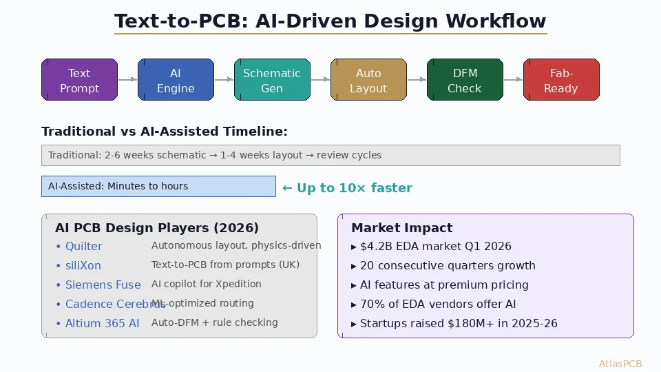
Text-to-PCB: How Generative AI Is Disrupting Circuit Board Design in 2026
From siliXon's text-prompt PCB generation to Quilter's autonomous layout and Siemens Fuse AI agents—explore how generative AI is transforming electronic design automation and what it means for hardware engineers.
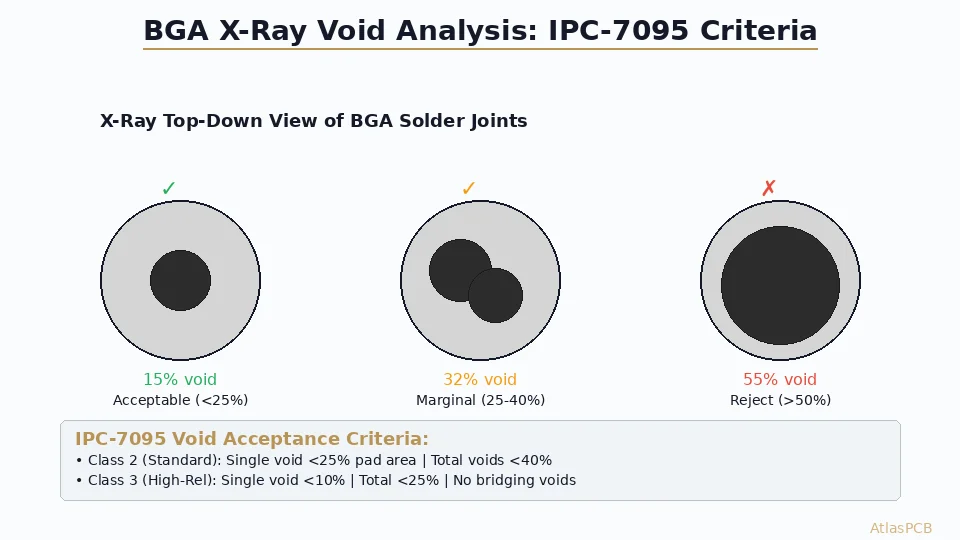
BGA X-Ray Void Analysis: IPC-7095 Acceptance Criteria and Inspection Best Practices
Master BGA solder joint void analysis using X-ray inspection. Understand IPC-7095 acceptance criteria, void percentage calculations, and how to distinguish process voids from reliability-threatening defects.
Edge AI PCB Design: Thermal Management, Signal Integrity, and Power Delivery for NPU Hardware in 2026
Explore the unique PCB design challenges of edge AI hardware — from thermal via arrays managing 25W NPU chips in constrained form factors to DDR5/LPDDR5X routing and multi-rail power delivery networks for 45-80 TOPS AI accelerators.
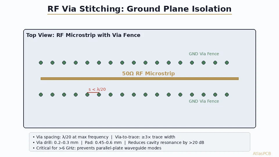
RF Via Stitching and Ground Plane Isolation: Preventing Cavity Resonance in High-Frequency PCB Design
Learn how via stitching creates effective Faraday cage isolation for RF signals, preventing parallel-plate waveguide modes and cavity resonance in PCB designs above 6 GHz.
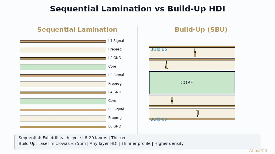
Sequential Lamination vs Build-Up HDI: Choosing the Right Process for High-Density PCB Design
Compare sequential lamination and SBU build-up processes for HDI PCBs. Learn when each approach delivers optimal density, reliability, and cost for your multilayer design.
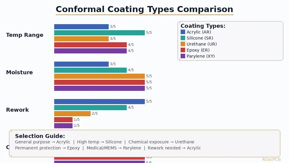
PCB Conformal Coating Selection Guide: Types, IPC Standards, and Application Methods for Electronics Protection
Complete guide to PCB conformal coating selection. Compare acrylic, silicone, urethane, epoxy, and parylene coatings. Learn IPC-CC-830B testing, application methods, and design rules for reliable electronics protection.
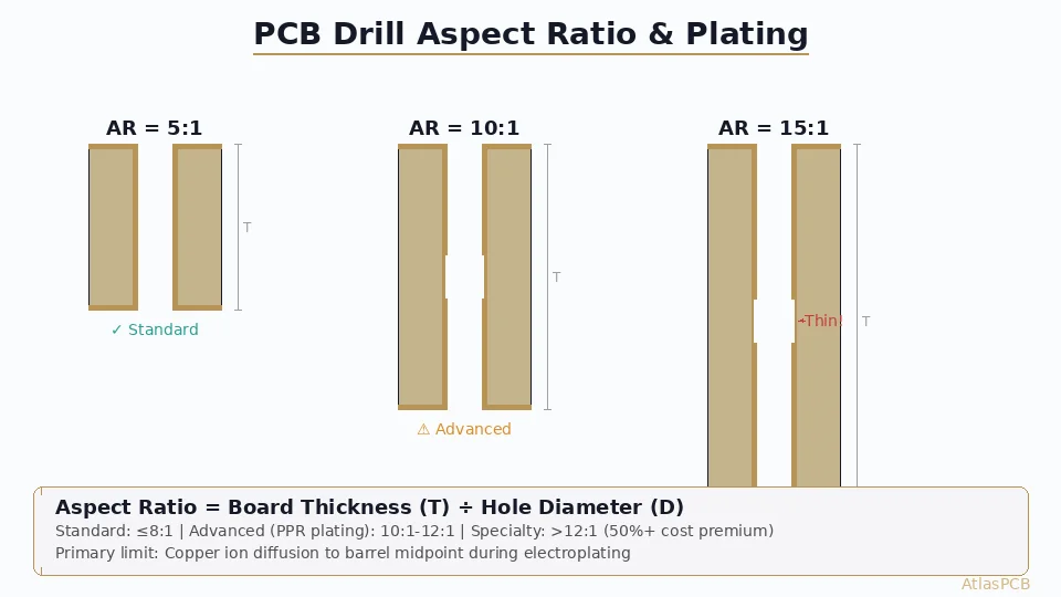
PCB Aspect Ratio in Drilling: Design Limits, Manufacturing Challenges, and Solutions for High-Layer-Count Boards
Understand PCB drill aspect ratio limits and their impact on plating quality. Learn IPC guidelines, mechanical vs laser drilling capabilities, and design strategies for reliable high-aspect-ratio vias in thick multilayer boards.
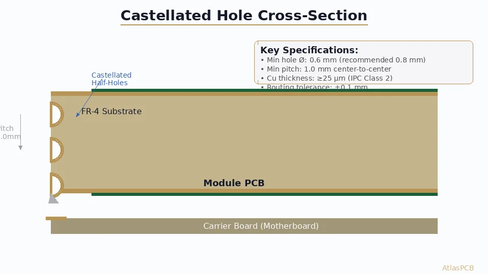
PCB Edge Plating and Castellated Holes: Complete Guide to Module-Ready Board Design
Master PCB edge plating and castellated hole design for modular electronics. Learn manufacturing processes, IPC specifications, design rules, and solderability requirements for reliable board-to-board connections.
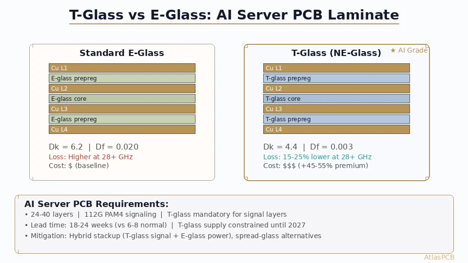
T-Glass Shortage Threatens AI Server PCB Production: Why Next-Gen Laminates Are the Bottleneck for Data Center Expansion
The global shortage of T-glass (NE-glass) fiber for ultra-low-loss PCB laminates is emerging as a critical bottleneck for AI server and data center infrastructure. With AI accelerator PCBs requiring 20+ layers of premium laminate, T-glass supply constraints may limit hyperscaler buildout through 2027.
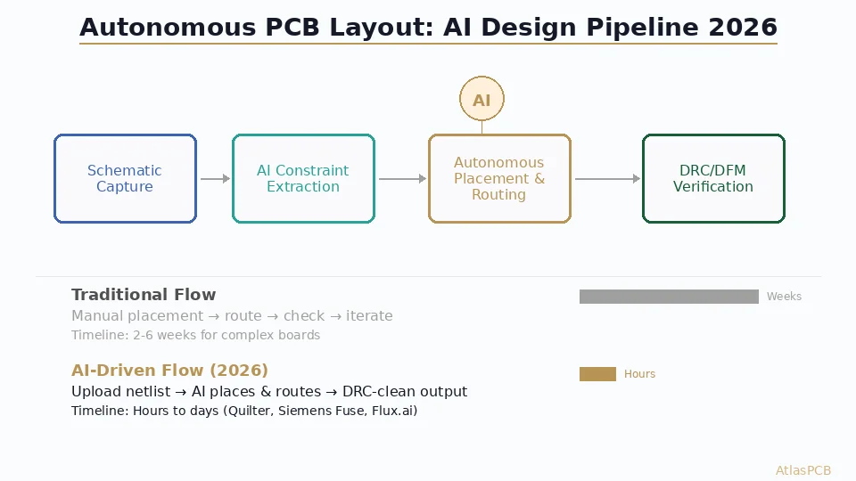
Autonomous PCB Layout in 2026: How Quilter, Siemens Fuse, and Flux.ai Are Eliminating Weeks from Hardware Development
Autonomous PCB layout tools have matured from research demos to production-ready systems. This deep-dive compares Quilter's physics-based routing, Siemens Fuse AI agents, and Flux.ai's cloud-native approach — analyzing where each excels and what it means for PCB fabrication.
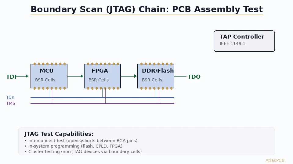
Boundary Scan (JTAG) Testing for PCB Assembly: IEEE 1149.1 Implementation, DFT Guidelines, and Fault Coverage
Learn how boundary scan (JTAG/IEEE 1149.1) testing verifies PCB assembly integrity, detects BGA opens and shorts without physical access, and integrates with flying probe and ICT for maximum fault coverage.
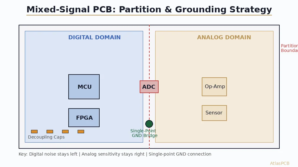
Mixed-Signal PCB Layout: Grounding, Partition Strategies, and Noise Isolation for ADC/DAC Systems
Master mixed-signal PCB design with proven partition strategies, single-point grounding, guard traces, and analog-digital isolation techniques for high-resolution ADC/DAC applications.
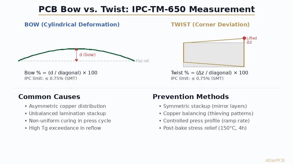
PCB Bow and Twist: IPC-TM-650 Measurement Methods, Causes, and Prevention Strategies
Understand PCB bow and twist according to IPC-TM-650 standards, learn measurement techniques, root causes in lamination and copper distribution, and proven prevention methods for SMT-compatible flatness.
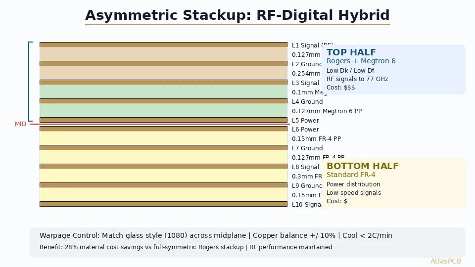
Asymmetric PCB Stackups: When Breaking Symmetry Improves High-Speed Performance
Learn when and why asymmetric PCB stackups outperform symmetric designs in high-speed, RF-digital hybrid, and thermal management applications — with practical layer assignment strategies and warpage mitigation techniques.
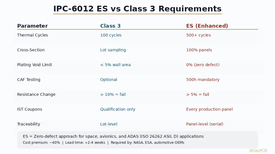
IPC-6012 ES Class: Enhanced Reliability Requirements for Automotive and Aerospace PCBs
Deep-dive into IPC-6012 ES (Space and Military Avionics) addendum requirements — from microsection criteria to thermal cycling endurance — and how they compare to standard Class 3 specifications.
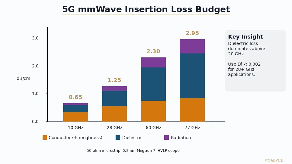
RF Transmission Line Loss Budgeting: Calculating Insertion Loss for 5G mmWave PCBs
Master insertion loss budgeting for 5G mmWave PCB designs. Learn how conductor loss, dielectric loss, and radiation loss interact at 28–77 GHz, with practical stackup and material selection strategies.
Siemens Xpedition Standard: AI-Driven PCB Design Automation Comes to SMB Teams
Siemens' new Xpedition Standard and PADS Pro Essentials bring enterprise-grade AI PCB design automation to small and mid-sized teams — a shift that democratizes intelligent routing, design reuse, and DFM-connected workflows.
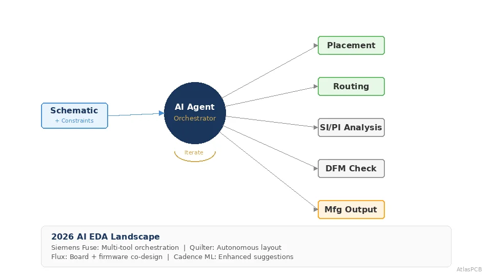
AI-Powered EDA Tools in 2026: How Autonomous Agents Are Reshaping PCB Design from Schematic to Fabrication
Explore how AI-powered EDA tools from Siemens Fuse, Quilter, Flux, and Cadence are transforming PCB design in 2026. Learn how autonomous AI agents handle placement, routing, DFM verification, and signal integrity analysis — and what this means for hardware engineers and PCB manufacturers.
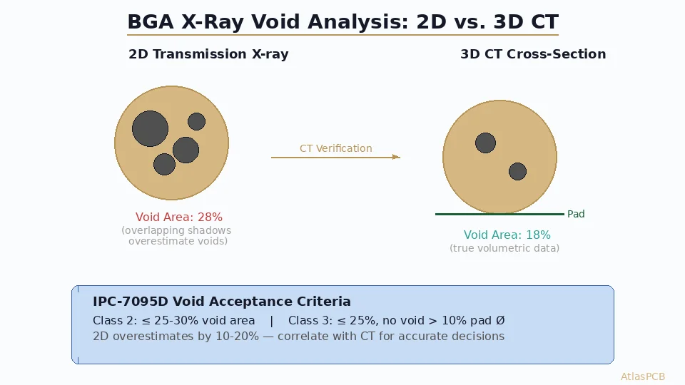
BGA X-Ray Void Analysis: Inspection Methods, IPC-7095 Criteria, and Defect Classification for High-Reliability Assembly
Learn how to perform BGA X-ray void analysis using 2D transmission and 3D CT inspection. Understand IPC-7095 acceptance criteria, void percentage calculation methods, defect classification, and practical thresholds for Class 2 and Class 3 assemblies.
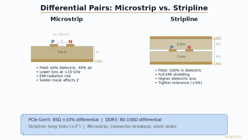
Differential Impedance Control for PCIe Gen5 and DDR5: Microstrip vs. Stripline Routing Strategies
Master differential impedance control for PCIe Gen5 (32 GT/s) and DDR5 (6400+ MT/s) interfaces. Compare microstrip and stripline routing, understand coupling effects, design stackups for 85Ω and 100Ω differential impedance, and learn practical tolerance budgeting for high-speed SerDes signaling.
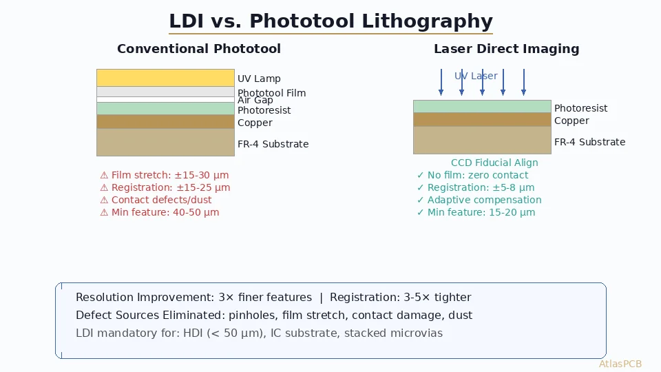
PCB Laser Direct Imaging (LDI): Resolution Advantages Over Phototool Lithography for Fine-Pitch HDI Manufacturing
Compare PCB laser direct imaging (LDI) with conventional phototool lithography. Learn how LDI achieves 15μm line/space resolution without film registration errors, reduces DES defects, and enables cost-effective fine-pitch HDI and IC substrate manufacturing.
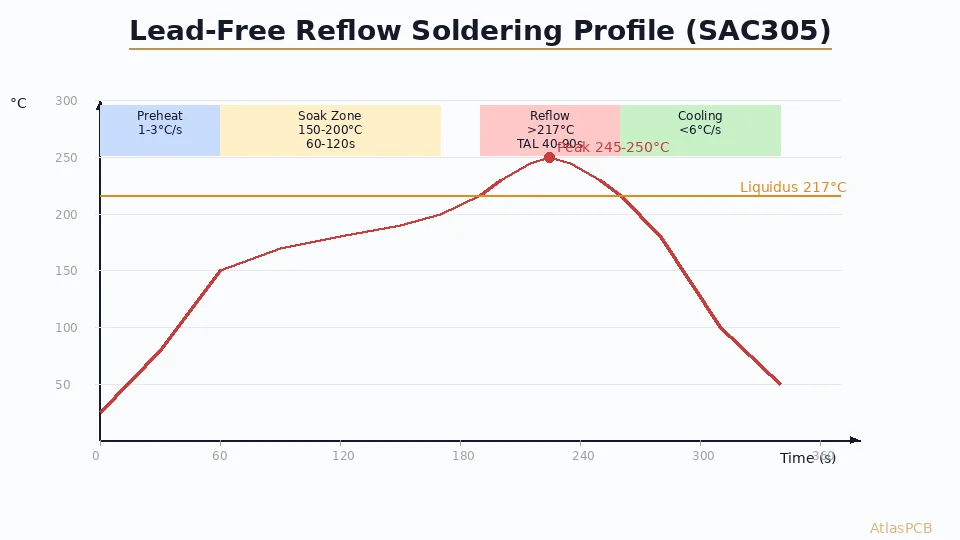
PCB Reflow Oven Profiling: Peak Temperature, Soak Time, and Defect Prevention for BGA Assembly
Master reflow soldering profile optimization for lead-free BGA assembly — covering preheat ramps, soak zone parameters, time above liquidus, peak temperature limits, and common reflow defects with prevention strategies.
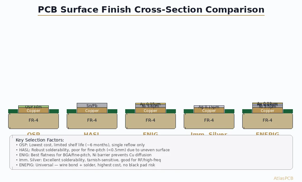
OSP vs ENIG vs Immersion Silver: How to Choose PCB Surface Finish for Lead-Free Assembly
A practical engineering guide comparing OSP, HASL, ENIG, immersion silver, and ENEPIG surface finishes for lead-free PCB assembly — covering solderability, shelf life, cost, and fine-pitch compatibility.
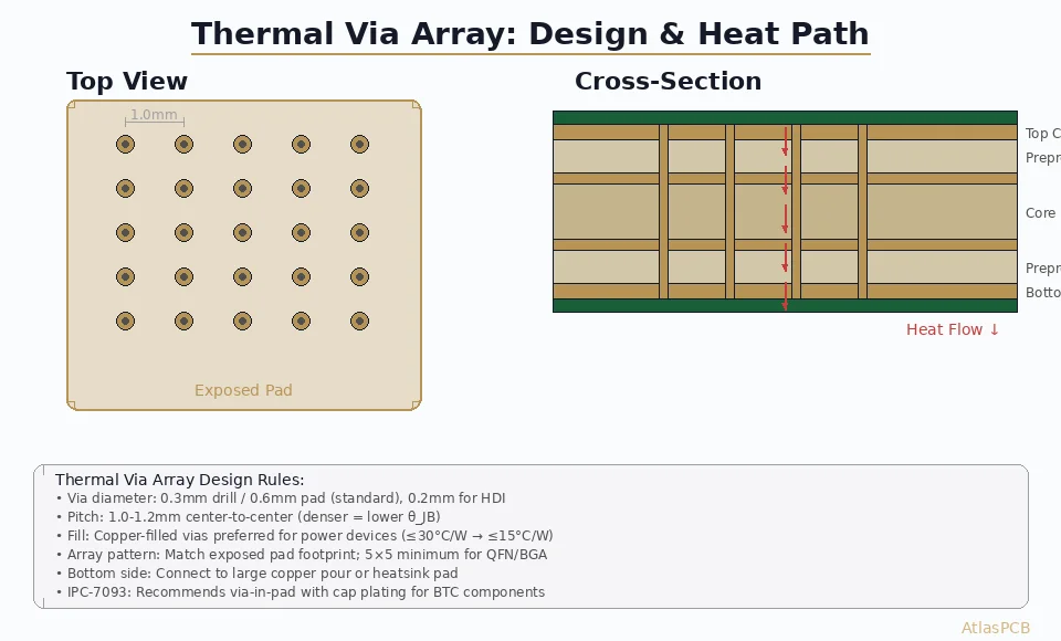
PCB Thermal Via Arrays: Design Rules, Copper Fill, and Heat Dissipation for Power Electronics
Engineering guide to designing thermal via arrays for effective heat transfer in power PCBs — covering via diameter, pitch, fill options, array patterns, and thermal resistance calculations for QFN, BGA, and power module packages.
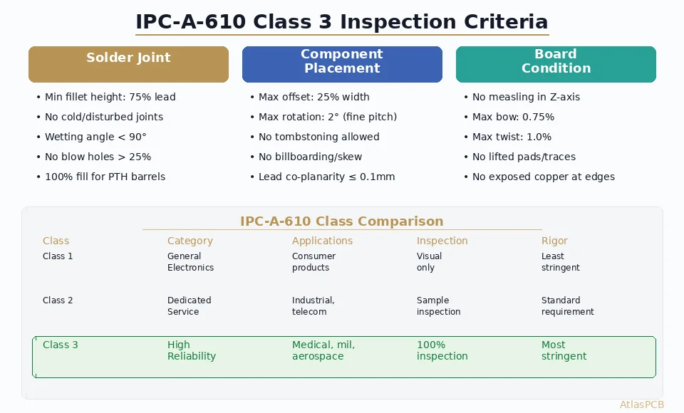
IPC-A-610 Class 3 Inspection: Workmanship Standards for High-Reliability PCB Assembly
Complete guide to IPC-A-610 Class 3 inspection criteria for solder joints, component placement, cleanliness, and board condition. Learn the specific accept/reject criteria that separate high-reliability assemblies from standard products.
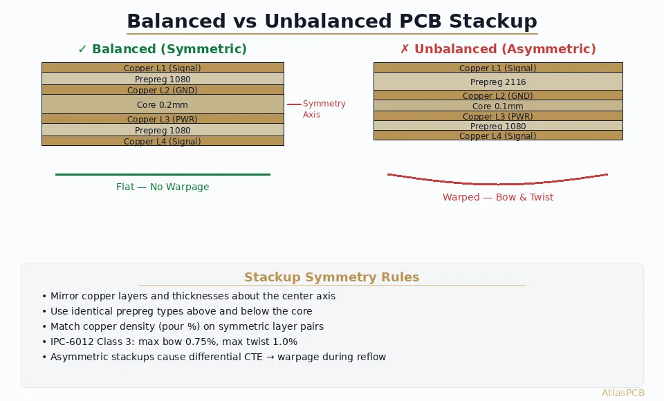
PCB Stackup Symmetry: Why Balanced Lamination Prevents Warpage in Multilayer Boards
Learn why stackup symmetry is critical for multilayer PCB reliability. This guide covers balanced lamination rules, CTE-driven warpage mechanisms, copper balancing techniques, and IPC-6012 bow/twist specifications with practical stackup examples.
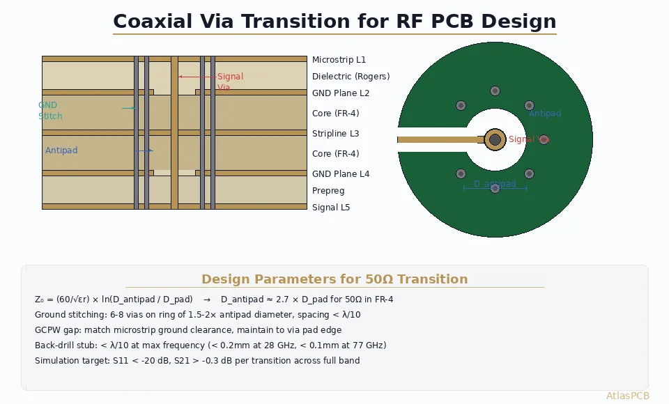
PCB Via Transitions in RF Design: Coaxial Via, GCPW, and Antipad Optimization for mmWave Signals
Master RF via transitions from microstrip to stripline. Learn coaxial via structures, GCPW launch design, antipad sizing, and ground stitching techniques for minimal signal loss at 5G and mmWave frequencies.
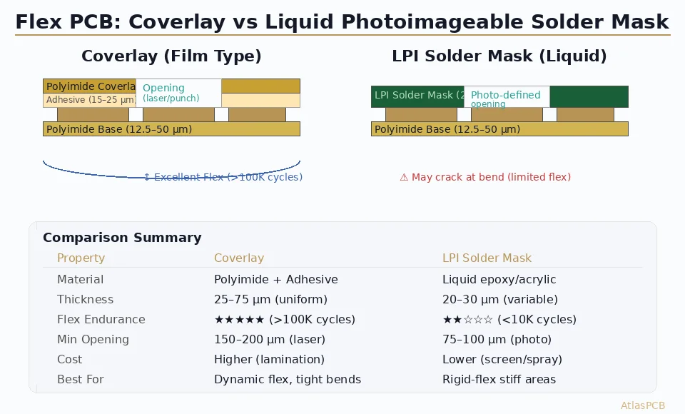
Flex PCB Coverlay vs Solder Mask: Material Selection, Design Rules, and Bend Reliability
Comprehensive comparison of coverlay film and liquid photoimageable (LPI) solder mask for flex and rigid-flex PCBs — covering material properties, opening tolerances, bend endurance, cost trade-offs, and IPC-6013 compliance.
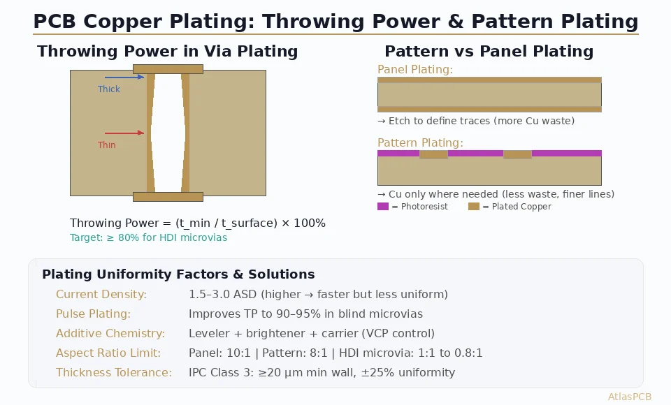
PCB Copper Plating Uniformity: Throwing Power, Pattern Plating, and HDI Via Fill
In-depth guide to achieving uniform copper plating on PCBs — covering throwing power optimization, pattern vs panel plating trade-offs, pulse plating for HDI via fill, additive chemistry control, and IPC-6012 thickness requirements.
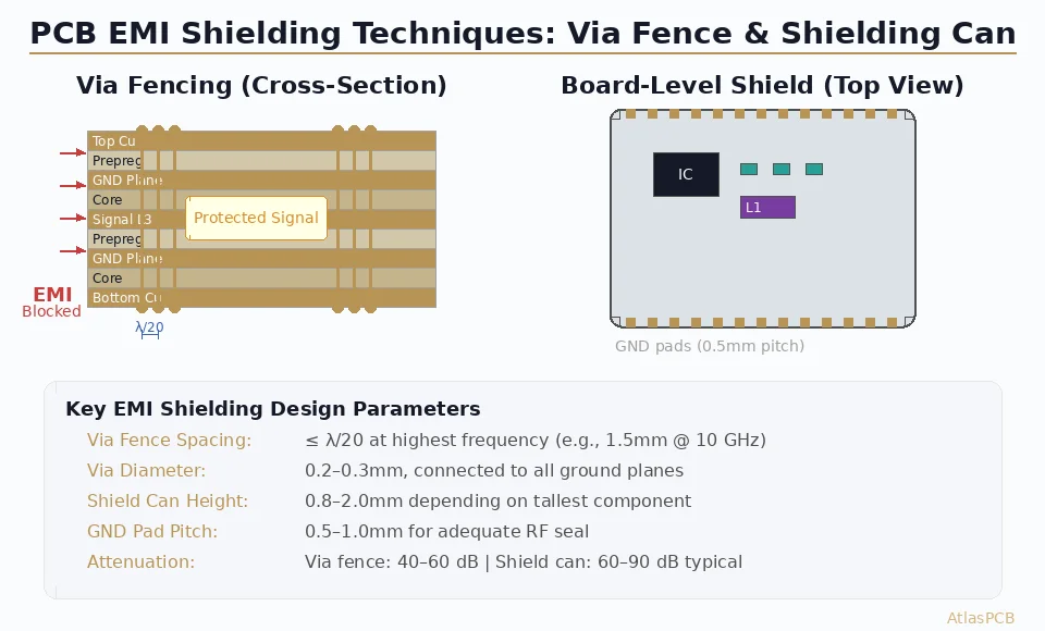
PCB EMI Shielding: Via Fencing, Board-Level Shield Cans, and Grounding Strategies
Complete guide to PCB-level EMI shielding techniques including via fencing design rules, board-level shielding can selection, grounding strategies, and IPC/FCC compliance for mixed-signal and RF designs.
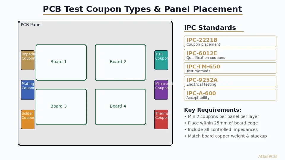
PCB Test Coupon Design: IPC Standards, Types & Best Practices
Complete engineering guide to PCB test coupon design per IPC-2221B, IPC-6012E, and IPC-TM-650. Covers impedance coupons, plating coupons, microsection coupons, and panel placement strategies for quality verification.
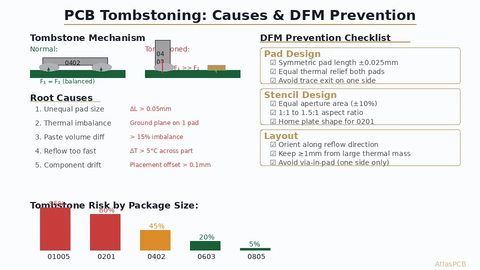
PCB Tombstoning: Causes, Prevention & DFM Design Checklist
Engineering-focused guide to eliminating tombstoning defects through PCB design. Covers root cause physics, pad geometry rules, thermal balancing, stencil optimization, and a complete DFM checklist for 0201 and 01005 components.
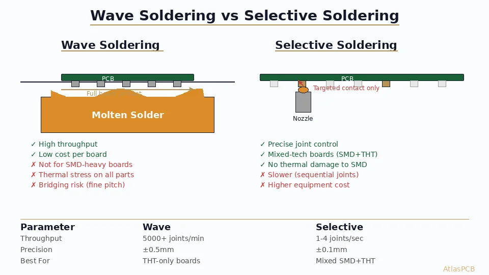
Wave Soldering vs Selective Soldering for PCB Assembly: Complete Comparison
In-depth engineering comparison of wave soldering and selective soldering for PCB assembly. Covers process mechanics, throughput, cost analysis, defect profiles, and when to specify each technology for THT and mixed-technology boards.
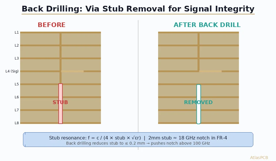
PCB Back Drilling (Controlled-Depth Drilling): Via Stub Removal for 10+ Gbps Signal Integrity
Complete guide to PCB back drilling for via stub removal. Learn stub resonance calculations, drill depth tolerances, IPC specifications, and when back drilling is essential for 10+ Gbps SerDes channels.
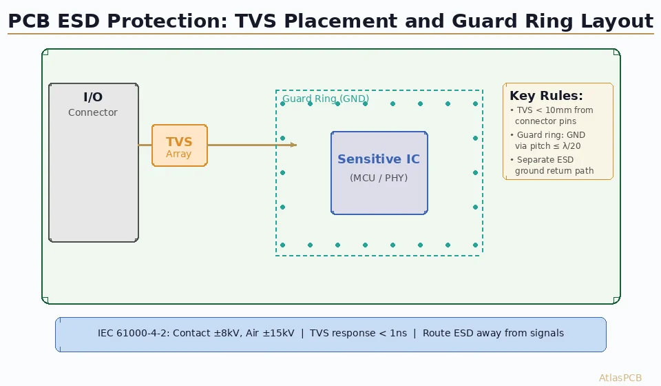
PCB ESD Protection Design: TVS Selection, Guard Ring Layout, and IEC 61000-4-2 Compliance
Complete guide to PCB-level ESD protection design. Learn TVS diode selection, guard ring layout, trace routing rules, and testing methods per IEC 61000-4-2 and IPC standards for robust electronics.
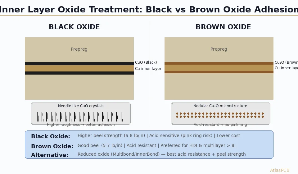
PCB Inner Layer Oxide Treatment: Black Oxide vs Brown Oxide Adhesion for Multilayer Reliability
Compare black oxide (CuO) and brown oxide (Cu₂O) treatments for PCB inner layer adhesion. Learn peel strength data, pink ring prevention, reduced oxide alternatives, and IPC-TM-650 testing methods.
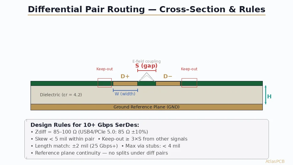
Differential Pair Routing Rules for 10+ Gbps SerDes: PCIe 5.0, USB4, and Beyond
Master differential pair routing for high-speed SerDes interfaces. Complete design rules for impedance control, length matching, via transitions, and reference plane management at 10-32 Gbps.
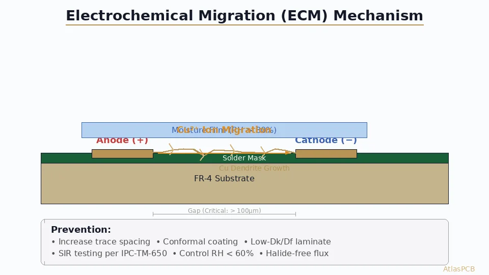
PCB Electrochemical Migration (ECM): Causes, Testing, and Prevention Strategies
Electrochemical migration causes dendritic shorts in humid environments. Learn how to prevent ECM failures through material selection, design rules, and IPC-compliant SIR testing.
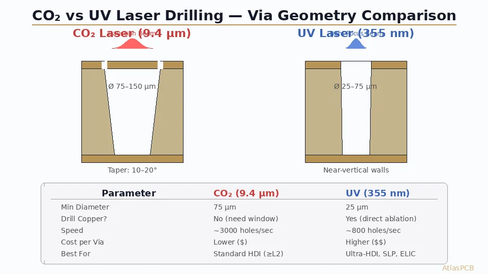
PCB Laser Drilling: CO₂ vs UV Parameters for Optimal Microvia Quality
Compare CO₂ and UV laser drilling for PCB microvias. Detailed parameter guides for pulse energy, repetition rate, focus control, and quality metrics including taper angle, smear, and copper damage.
IPC-A-600 PCB Acceptability Standard: Complete Visual Inspection Criteria and Classification Guide
Master IPC-A-600 acceptability criteria for bare PCB inspection. This comprehensive guide covers Class 1/2/3 requirements, common defect types, acceptance/rejection criteria for conductors, holes, surface finish, and solder mask — essential knowledge for quality engineers and procurement teams.
PCB Power Integrity Design: Decoupling Capacitor Placement, PDN Impedance, and Voltage Droop Prevention
Complete guide to PCB power delivery network (PDN) design covering decoupling capacitor selection and placement, target impedance calculation, power plane cavity resonance, and practical voltage droop prevention strategies for high-speed digital systems operating at 1V and below.

PCB Solder Mask: Types, Application Methods, Thickness Control, and DFM Best Practices
Everything engineers need to know about PCB solder mask — from LPI and dry film types to application methods, dam design rules, thickness specifications, registration tolerances, and DFM optimization. Covers IPC-SM-840 requirements and practical troubleshooting for fine-pitch BGA designs.
Aluminum PCB Thermal Design for High-Power LED and Motor Drivers: Material Selection, Stackup, and DFM Guide
Complete guide to aluminum PCB (metal-core PCB) thermal design covering aluminum alloy selection, dielectric layer optimization, thermal conductivity calculations, LED array layout, motor driver thermal management, and DFM rules for manufacturing reliability.
Any-Layer HDI PCB Design: When to Go Beyond 2+N+2 and How to Optimize for Wearables and SiP Modules
Advanced guide to any-layer HDI PCB design covering when to use ALIS (any-layer interconnect structure) vs standard HDI buildups, microvia stacking strategies, cost drivers, material selection for ultra-thin substrates, and design optimization for wearable electronics and System-in-Package modules.

PCB Panelization and Array Design: V-Score vs Tab Routing, DFM Rules, and Cost Optimization
Complete PCB panelization guide covering V-score vs tab routing vs jump scoring, panel size optimization for SMT lines, fiducial placement, tooling strip design, breakaway tab rules, and DFM best practices to maximize yield and minimize assembly cost.
BGA Pad Design and Via-in-Pad: How to Prevent Solder Voiding in High Pin-Count BGA Assemblies
Master BGA pad design with via-in-pad plating techniques. Learn NSMD vs SMD pad strategies, via fill requirements, IPC-7095 compliance, and proven methods to achieve less than 25% voiding under 0.4mm-pitch BGAs.

mmWave PCB Material Selection: Rogers vs Megtron vs LCP for 5G and 6G Applications
Compare Rogers 3003/4350B, Panasonic Megtron 7, and Liquid Crystal Polymer (LCP) for millimeter-wave PCB designs. Learn dissipation factor, Dk stability, moisture absorption, and cost trade-offs for 28-77 GHz 5G/6G antenna and front-end modules.
Rigid-Flex PCB Design Guide: Bend Radius, Layer Transitions, and Reliability for Wearables and Aerospace
Complete rigid-flex PCB design guide covering bend radius calculations, flex-to-rigid transition zones, copper type selection, coverlay vs solder mask, IPC-2223 compliance, and reliability testing for dynamic and static flex applications.
Controlled Impedance PCB Design: Stack-Up Calculations, Tolerance Analysis, and Manufacturing Guide
Master controlled impedance PCB design from first principles. Learn impedance calculation formulas, stack-up optimization for 50Ω/100Ω targets, dielectric material selection, trace geometry rules, TDR measurement, and manufacturing tolerance budgets for high-speed digital and RF applications.
IPC-2581 Digital Twin: PCB Data Exchange Standard for Smart Manufacturing and Industry 4.0
Complete guide to IPC-2581 — the intelligent PCB data exchange standard enabling digital twins, automated DFM, and lights-out manufacturing. Learn how IPC-2581 replaces Gerber files, its structure, adoption benefits, and implementation for PCB design-to-manufacturing workflows.
PCB Design for GaN and SiC Power Devices: Thermal Management, Layout Rules, and Material Selection
Complete guide to PCB design for gallium nitride (GaN) and silicon carbide (SiC) wide-bandgap power devices. Learn thermal via arrays, copper weight selection, creepage requirements, and high-frequency layout techniques for EV inverters, data center power, and industrial drives.

AOI and SPI Inspection in PCB Assembly: Automated Optical Inspection Technology for Zero-Defect Manufacturing
Complete guide to AOI and SPI inspection systems in PCB assembly. Covers solder paste inspection principles, automated optical inspection algorithms, 3D measurement technology, defect classification, programming strategies, and integration with Industry 4.0 traceability systems.

IC Substrate vs HDI PCB: Understanding Substrate-Like PCB (SLP) Technology for Advanced Semiconductor Packaging
Deep technical comparison of IC substrates, HDI PCBs, and substrate-like PCBs (SLP). Learn the manufacturing differences, design rules, material systems, and application boundaries as advanced packaging blurs the line between PCB fabrication and semiconductor packaging.

Reflow Soldering Profile Optimization: Lead-Free PCB Assembly Temperature Profiles for SAC305 and Beyond
Master reflow soldering profile optimization for lead-free PCB assembly. Learn thermal profiling zones, SAC305 peak temperature windows, ramp rates, and troubleshooting techniques for zero-defect BGA, QFN, and fine-pitch component soldering.

PCB Copper Plating Process: Electroless vs Electrolytic Copper for HDI Vias and High-Density Interconnects
Compare electroless and electrolytic copper plating processes for HDI PCB manufacturing. Learn desmear preparation, plating chemistry, via fill techniques, and quality metrics that determine microvia reliability in advanced multilayer boards.
PCB Ground Plane Design: Reducing EMI and Ground Bounce in High-Speed Digital Circuits
Master PCB ground plane design techniques for high-speed digital circuits. Learn split-plane strategies, via stitching, decoupling capacitor placement, and stack-up optimization to minimize EMI radiation and ground bounce noise.

PCB Surface Finish Comparison: OSP vs HASL vs Immersion Silver vs ENIG for Assembly Reliability
In-depth comparison of PCB surface finishes—OSP, HASL, Immersion Silver, and ENIG—covering solderability, shelf life, wire bonding capability, fine-pitch compatibility, and total cost of ownership for different assembly requirements.
BGA Rework and Reballing: Complete Process Guide for High-Reliability PCBs
Master BGA rework and reballing techniques for high-reliability PCB assemblies. Learn proper thermal profiling, flux selection, pad preparation, and IPC-7095 compliance for aerospace, medical, and automotive applications.
IPC-6013 Flexible Circuit Quality Standard: Design Rules and Acceptance Criteria
Complete guide to IPC-6013 qualification requirements for flexible and rigid-flex PCBs. Covers Class 1/2/3 acceptance criteria, bend radius rules, conductor spacing, coverlay requirements, and testing protocols for flex circuit manufacturing.
PCB Solder Mask Application: LPI vs Dry Film vs Inkjet Processes Compared
Compare PCB solder mask application methods—liquid photoimageable (LPI), dry film, and inkjet—with detailed analysis of resolution capability, thickness control, cost factors, and suitability for HDI, flex, and high-frequency applications.
Controlled Impedance PCB Stackup Design: Rules, Calculations, and Manufacturing Tolerances for High-Speed Designs
Master controlled impedance PCB stackup design with practical rules for microstrip, stripline, and differential pair geometries. Covers impedance calculation methods, manufacturing tolerances, and material selection for designs from 1 Gbps to 112 Gbps PAM4.
ENEPIG vs ENIG Surface Finish: Complete Comparison for Wire Bonding, Solderability, and Long-Term Reliability
Compare ENEPIG and ENIG PCB surface finishes for wire bonding, BGA soldering, and press-fit applications. Covers nickel corrosion risks, gold thickness specifications, palladium's role, cost analysis, and selection guidelines for aerospace, automotive, and consumer electronics.
IPC-A-600 Class 2 vs Class 3: PCB Acceptability Criteria, Defect Classification, and When to Specify Each Class
Understand IPC-A-600 PCB acceptability criteria differences between Class 2 and Class 3. Covers defect classification for annular ring, plating voids, copper thickness, laminate conditions, and marking — with practical guidance on when each class applies to your product.
AI Hardware PCB Thermal Management: Advanced Multilayer Stackup Design for 1000W+ Processing Units
Master thermal management in multilayer PCBs for AI hardware. Learn advanced stackup techniques, copper balancing, and thermal via design for 1000W+ GPU/TPU applications with proper heat dissipation.
RF PCB Material Selection for Automotive Radar: Rogers vs PTFE Performance Analysis at 77-81 GHz
Compare Rogers and PTFE materials for automotive radar PCBs. Analyze dielectric properties, loss tangent, and thermal performance for 77-81 GHz ADAS applications in harsh automotive environments.
DFM for Fine-Pitch BGA: PCB Design Rules That Prevent Assembly Defects
Master DFM rules for fine-pitch BGA packages (≤0.5mm pitch). Covers pad design, solder mask opening, via-in-pad requirements, and common assembly defects with prevention strategies.
HDI PCB Design for 5G Antenna Integration: Signal Integrity Challenges in Millimeter-Wave Applications
Master HDI PCB design techniques for 5G antenna integration. Learn signal integrity optimization, substrate selection, and routing strategies for millimeter-wave frequencies up to 71 GHz.
Microvia Reliability in HDI PCBs: Stacked vs Staggered Configurations for High-Density Designs
Compare stacked and staggered microvia configurations in HDI PCBs. Learn reliability differences, IPC guidelines, and when each approach best serves your high-density interconnect design.
Rogers vs PTFE Laminates for RF PCB Design: Material Selection Guide for 5G and mmWave Applications
Compare Rogers 4350B, 4003C, RT/duroid, and generic PTFE laminates for RF PCB applications. Covers Dk/Df, thermal stability, processability, and cost considerations for 5G and mmWave designs.
PCB Electroless Copper Plating: Chemistry, Process Steps, and Quality Control
Deep dive into PCB electroless copper plating — from palladium activation chemistry to deposition control, void prevention, and IPC standards for through-hole metallization.
PCB Thermal Relief Pad Design: Spoke Patterns, Anti-Pad Sizing, and DFM Best Practices
Master PCB thermal relief pad design with guidelines on spoke patterns, anti-pad sizing, direct connections vs thermal reliefs, and IPC-compliant DFM rules.
HDI Via Reliability Under Thermal Cycling: Testing, Failure Modes & Design Guidelines
Learn how HDI microvias perform under thermal cycling stress. Explore failure mechanisms, IPC testing standards, and design strategies for maximum via reliability.

Multilayer PCB Warpage Simulation: FEA Methods, IPC Standards & Design Control
Learn how to predict and control PCB warpage using FEA simulation. Covers IPC bow/twist specs, copper balancing, and process optimization for multilayer boards.

PCB Fiber Weave Effect on Signal Skew: Causes, Impact & Mitigation for High-Speed Design
Understand how glass fiber weave patterns cause signal skew in high-speed PCBs. Learn mitigation techniques including trace rotation, spread glass, and material selection.

PCB Plasma Desmear Process: Technology, Parameters & Advantages Over Chemical Desmear
Explore PCB plasma desmear technology for via cleaning. Compare plasma vs. permanganate desmear, learn process parameters, and discover when plasma treatment is essential.
PTFE Substrate Handling & Fabrication: Challenges and Best Practices for RF PCBs
Master PTFE substrate fabrication for RF PCBs. Learn handling, drilling, lamination, and plating techniques to overcome Teflon's unique manufacturing challenges.
High-Speed Backplane PCB Design: Signal Integrity, Material Selection & Layout Best Practices
Master high-speed backplane PCB design with proven strategies for signal integrity, material selection, impedance control, and differential pair routing in multi-gigabit systems.
PCB Dielectric Constant (Dk) Measurement: Methods, Accuracy & Impact on Impedance Control
Understand PCB dielectric constant measurement methods, accuracy factors, and how Dk variations affect impedance control in high-frequency circuit board design.
PCB Ground Plane Stitching Vias: Placement Rules, EMI Reduction & High-Speed Design Guidelines
Learn PCB ground plane stitching via placement rules, spacing calculations, and EMI reduction strategies for high-speed and high-frequency circuit board designs.
PCB Rigid-Flex Bend Zone Reliability: Design Rules, Material Selection & Lifecycle Testing
Ensure PCB rigid-flex bend zone reliability with expert guidance on bend radius rules, material selection, copper treatment, and lifecycle testing for flex circuits.
PCB Solder Paste Stencil Design: Aperture Rules, Thickness Selection & Print Quality Optimization
Optimize PCB solder paste stencil design with expert guidance on aperture sizing, stencil thickness, area ratio rules, and print quality for reliable SMT assembly.
Dynamic Flex PCB Design — Bend Radius, Material Selection, and Reliability
A comprehensive engineering guide to dynamic flex PCB design, covering minimum bend radius formulas, rolled annealed vs electrodeposited copper, adhesiveless constructions, stiffener design, IPC-2223 requirements, fatigue life testing, and real-world applications.
PCB Bow and Twist: IPC Specification, Measurement Methods & Prevention
Comprehensive guide to PCB bow and twist covering IPC-6012 specifications, TM-650 measurement methods, root causes, prevention strategies, and the impact of warpage on SMT assembly reliability.
Buried Via Technology in High-Density PCBs: Design Rules, Fabrication & Cost
Comprehensive guide to buried via technology in HDI PCBs. Learn design rules, fabrication sequences, cost drivers, and when buried vias outperform through-hole alternatives.
Castellated Holes in PCBs: Design Rules, Plating Requirements & Module Applications
Complete guide to castellated hole PCB design covering half-hole plating specifications, design rules for module boards, soldering requirements, and IPC quality standards for castellation.
PCB Copper Pour and Ground Plane Design: Best Practices for Signal Integrity
Master copper pour and ground plane design for EMI shielding and signal integrity. Learn ground plane partitioning, stitching vias, clearance rules, and thermal relief strategies.
PCB Drilling Aspect Ratio Limits: Mechanical vs Laser Drill Capabilities
Understand PCB drill aspect ratio limits for mechanical and laser drilling. Learn how hole diameter, board thickness, and drill technology affect via reliability and manufacturability.
Laser Direct Imaging (LDI) in PCB Manufacturing: Accuracy, Benefits & When to Specify
Understand how Laser Direct Imaging (LDI) improves PCB accuracy over conventional photolithography. Learn LDI capabilities, fine-line requirements, and when to specify LDI for your design.
PCB Net Ties Explained: When and How to Use Them in Mixed-Signal Design
Learn what PCB net ties are, when to use them in mixed-signal and split-ground designs, and how to implement them correctly in your EDA tool for clean analog-digital separation.
Plated Through-Hole Reliability: Barrel Crack Prevention, IPC Testing & Design Rules
Learn how to prevent PTH barrel cracks through proper copper plating thickness, aspect ratio control, and IPC TM-650 testing. Expert design rules for thermally reliable plated through-holes.
Power Plane Design for PCB — Split Planes, Decoupling Strategy, and PDN Analysis
An advanced guide to PCB power distribution network design covering target impedance calculations, split plane rules, multi-tier decoupling strategies, via inductance management, cavity resonance, and practical PDN simulation workflows.
PCB电源平面设计 — 分割平面、去耦策略与PDN分析
深入指南:PCB电源分配网络设计,涵盖目标阻抗计算、分割平面规则、多层级去耦策略、过孔电感管理、腔体谐振以及实用PDN仿真工作流程。
Press-Fit Via Design for PCB Connectors: Hole Sizing, Plating & IPC Compliance
Expert guide to press-fit via design for PCB connectors covering compliant pin hole sizing, copper plating requirements, IPC-9797 compliance, and backplane design best practices.
PCB Silkscreen and Legend Design: Best Practices for Assembly and Traceability
Master PCB silkscreen design with best practices for reference designators, polarity markings, assembly instructions, and traceability. Includes IPC standards and DFM guidelines.
Solder Mask Dam Design — Rules, Tolerances, and DFM Best Practices
A comprehensive DFM guide to solder mask dam design covering minimum dam widths by technology, registration tolerances, SMD vs NSMD pad definitions, LPI vs dry film processes, BGA dam design for fine-pitch, via tenting, and IPC-SM-840 compliance.
阻焊坝设计 — 规则、公差与DFM最佳实践
全面的DFM指南:阻焊坝设计,涵盖各技术的最小坝宽、对位公差、SMD与NSMD焊盘定义、LPI与干膜工艺、细间距BGA坝设计、过孔盖油以及IPC-SM-840合规要求。
PCB Surface Finish Selection — ENIG vs HASL vs OSP vs Hard Gold vs ENEPIG
A comprehensive five-way comparison of the most common PCB surface finishes covering cost, reliability, solderability, wire bondability, and IPC standards compliance to help you choose the right finish for every application.
Buried Capacitance in PCBs: Embedded Layers for PDN
How embedded capacitor layers with ultra-thin dielectrics optimize power delivery networks and reduce discrete component count.
Controlled-Depth Drilling in PCBs Explained
Master controlled-depth drilling for back-drilling, blind vias, and depth-controlled routing in high-speed PCB designs.
PCB Etch Compensation: Trace Width Accuracy
How etch compensation maintains trace width accuracy in PCB production. Covers etch factor, copper weight effects, and fine-line DFM.
PCB Fabrication Tolerances: Engineering Spec Guide
Complete reference for PCB fabrication tolerances — drill, trace width, registration, impedance, and board thickness specifications.
High-Speed PCB Laminate Dk/Df Comparison
Compare Dk and Df values of Megtron 6, Rogers 4350B, Isola IS680, and Shengyi laminates for high-speed PCB design.
PCB Impedance Test Coupons: TDR Validation Guide
Design impedance test coupons for TDR validation with best practices for coupon layout, trace geometry, and measurement accuracy.
PCB Moisture Sensitivity and Baking Guidelines
Prevent delamination and popcorning with proper PCB baking procedures based on IPC-1601 moisture sensitivity levels.
Plating Void Prevention in PCB Vias
Causes, detection methods, and process controls for preventing plating voids in PCB through-hole and microvia plating.
Fine-Pitch SMT Pad Design: 0201 to BGA
Engineering guide to fine-pitch SMT pad design for 0201, 01005, and ultra-fine BGA landing patterns.
Via-in-Pad Plated Over (VIPPO) Design Guide
Complete guide to VIPPO technology covering via fill, copper capping, BGA fanout design rules, and manufacturing process steps.
16-Layer PCB Stackup Design: Rules, Impedance Planning & Material Selection
Complete engineering guide to 16-layer PCB stackup design. Covers layer assignment strategies, impedance planning, material selection for high-speed signals, power distribution, and manufacturing constraints for complex multilayer boards.
ENIG Surface Finish: Process, Thickness, and Common Defects
Deep dive into ENIG (Electroless Nickel Immersion Gold) PCB surface finish. Covers deposition process, thickness specifications, black pad defect prevention, solderability testing, and comparison with HASL, OSP, and ENEPIG alternatives.
High Tg PCB Material Selection Guide: TG150 vs TG170 vs TG180
Complete guide to high Tg PCB material selection. Compare TG150, TG170, and TG180 laminates for thermal reliability, lead-free compatibility, and cost optimization across industrial, automotive, and aerospace applications.
How Many Layers Does My PCB Need? A Decision Framework
Practical decision framework for PCB layer count selection. Covers signal density analysis, power distribution requirements, impedance control needs, and cost implications from 2-layer to 30+ layer designs.
How to Reduce PCB Crosstalk: Spacing Rules & Layout Techniques
Engineering guide to reducing PCB crosstalk. Covers near-end and far-end crosstalk mechanisms, 3W and 5W spacing rules, guard traces, stripline vs microstrip, stackup optimization, and simulation methodology for high-speed digital designs.
How to Specify Impedance on Your PCB: Stackup Notes & Fab Drawing Tips
Practical guide to specifying controlled impedance on PCB fabrication drawings. Covers impedance table format, stackup documentation, tolerance specifications, TDR coupon design, and communication best practices with your PCB manufacturer.
Medical PCB Manufacturing: FDA Compliance, Traceability & Reliability
Complete guide to medical PCB manufacturing requirements including FDA regulatory framework, IPC Class 3 specifications, full lot traceability, cleanliness standards, biocompatible materials, and sterilization compatibility for Class II and III medical devices.
Networking Switch PCB Design: High-Speed Signal Integrity, Material Selection, and Thermal Management
Engineering guide to designing PCBs for networking switches. Covers high-speed signal integrity for 25G/50G/100G+ interfaces, high-layer-count stackup strategy, low-loss material selection, and thermal management for data center switch applications.
PCB Annular Ring: Minimum Width Requirements per IPC Standards
Complete guide to PCB annular ring requirements including IPC-6012 Class 2 and Class 3 minimums, breakout rules, drill tolerance compensation, and design tips for laser-drilled vs mechanical vias.
PCB Aspect Ratio: Via Depth-to-Diameter Rules and Manufacturing Limits
A comprehensive guide to PCB via aspect ratios covering through-hole, blind, and buried vias. Learn IPC recommendations, manufacturing capability limits, and how aspect ratio impacts reliability.
CAF Resistance in PCBs: Conductive Anodic Filament Prevention and Design Rules
Comprehensive guide to Conductive Anodic Filament (CAF) formation in PCBs — the electrochemical migration mechanism along glass fibers, IPC-TM-650 test methods, design spacing rules, material selection strategies, and humidity effects on CAF resistance.
PCB Copper Plating: Thickness Uniformity, Specifications, and Quality Control
A comprehensive guide to PCB copper plating processes, including electroless and electrolytic plating, thickness uniformity challenges, IPC-6012 specifications, pulse plating technology, and plating void prevention strategies for reliable multilayer boards.
PCB Design for EMI Compliance: A Practical Guide to Passing Radiated and Conducted Emissions Tests
Learn how to design PCBs that pass EMI compliance testing. Covers grounding strategies, shielding techniques, filtering, component placement, and layout best practices for FCC, CE, and CISPR standards.
PCB Electrical Testing: Flying Probe vs Bed-of-Nails Fixture Testing Compared
A detailed comparison of flying probe and bed-of-nails fixture testing for PCB electrical verification. Understand when to use each method, their cost structures, test coverage differences, and how IPC-9252 defines net list testing requirements.
Hybrid PCB Stackup Design: Combining Rogers and FR4 for Cost-Effective RF Performance
Learn how hybrid PCB stackups combining Rogers high-frequency laminates with FR4 deliver excellent RF performance at a fraction of the cost of all-Rogers designs. This guide covers material selection, lamination challenges, CTE management, and practical design rules.
IPC-2581 vs Gerber: The Future of PCB Data Transfer
An in-depth comparison of IPC-2581 and Gerber formats for PCB manufacturing data exchange. Learn why the industry is moving toward intelligent, single-file data transfer and what it means for your design workflow.
PCB Laser Drilling: Microvia Technology, Parameters, and Quality Control
Comprehensive guide to PCB laser drilling technology covering CO2 vs UV laser systems, microvia formation processes, aspect ratio limits, desmear requirements, quality inspection methods, and comparison with mechanical drilling.
Resin Plug Via Process: When, Why, and How to Specify Filled Vias
Everything PCB designers need to know about resin-filled vias — from IPC-4761 fill types and via-in-pad requirements to planarization specifications, copper capping, and cost implications. A practical guide to specifying filled vias correctly.
PCB Via Size Guide: Mechanical, Laser & Microvia Dimensions
Complete guide to PCB via sizing covering mechanical drilled vias, laser-drilled microvias, and buried vias. Includes IPC aspect ratio rules, drill-to-copper clearances, annular ring requirements, and HDI via specifications.
PCB Warpage Control: Causes, IPC Limits, and Prevention in Multilayer Boards
In-depth guide to PCB warpage causes including CTE mismatch, copper imbalance, and reflow stress. Learn IPC-6012 warpage limits, copper balancing techniques, symmetric stackup design, and material selection strategies.
What Causes PCB Delamination? Root Causes, Prevention, and Quality Control
Understand the root causes of PCB delamination including moisture absorption, thermal stress, and material incompatibility. Learn prevention strategies, IPC inspection standards, and manufacturing process controls.
Rogers PCB Material Guide: Properties, Types & Manufacturer Selection
Complete overview of Rogers PCB materials including RO4000, RO3000, RT/duroid series. Compare Dk, Df properties, application ranges from 5G mmWave to automotive radar, and learn what to look for in a Rogers PCB manufacturer.
Embedded Component PCB Technology: Burying Passives and Actives Inside Substrates
A deep-dive into embedded component PCB technology — how resistors, capacitors, and even ICs are buried within substrate layers to slash parasitics, reclaim board space, and push high-frequency performance beyond surface-mount limits.
PCB Blind Via Fill Technology: Copper Plating, Epoxy Fill & IPC-4761 Type VII Explained
Complete engineering guide to blind via filling methods including electrolytic copper fill, conductive epoxy, and non-conductive epoxy. Covers IPC-4761 Type VII requirements, void-free fill criteria, dimple specifications, and via-in-pad design rules for HDI and BGA applications.
PCB Copper Balancing Techniques: Prevent Warpage in Multilayer Board Design
Learn copper balancing techniques for multilayer PCBs including thieving patterns, fill strategies, and IPC-6012 bow/twist requirements to prevent warpage during lamination and reflow.

PCB Edge Plating Guide: Castellation, EMI Shielding, and Wrap-Around Plating Design
Complete engineering guide to PCB edge plating techniques including castellation, wrap-around plating, and edge metallization for EMI shielding, RF grounding, and module interconnection. Covers IPC-6012 Class 3 requirements, manufacturing processes, and design rules.
PCB Gold Finger Connector Design: Hard Gold Plating, Beveling & IPC-6012 Requirements
Comprehensive engineering guide to PCB gold finger edge connector design covering hard gold plating specifications (30-50μin), nickel underplate requirements, beveling angles, dimensional tolerances, and IPC-6012 Section 3.6 acceptance criteria for PCIe, DIMM, and industrial backplane applications.

PCB Halogen-Free Materials Guide: IEC 61249, IPC-4101E Compliance and Material Selection for 2026
Complete guide to halogen-free PCB materials covering IEC 61249-2-21 definitions, IPC-4101E slash sheet requirements, phosphorus vs nitrogen flame retardants, and practical material selection for environmental compliance.
PCB Power Integrity and Decoupling: Complete PDN Design Guide for High-Speed Digital Systems
Master Power Distribution Network design with target impedance calculations, decoupling capacitor selection strategies, and PDN simulation techniques for FPGA, SoC, and high-speed digital PCBs.
PCB Thermal Via Design: Engineering Guide to Heat Dissipation Through Via Arrays
Complete engineering guide to thermal via design for power components. Covers via diameter and pitch calculations, IPC-2152 thermal guidelines, thermal resistance formulas, filled vs unfilled vias, and ANSYS simulation best practices.
PCB Tombstoning Prevention: A Complete SMT Design and Process Guide
Comprehensive engineering guide to preventing tombstoning (Manhattan effect) in SMT assembly — covering pad design symmetry per IPC-7351B, thermal balancing, stencil design per IPC-7525, reflow profile optimization, and DFM strategies for 0201/01005 components.
Press-Fit Connector PCB Design: Complete Engineering Guide to Compliant Pin Technology
Master press-fit connector PCB design with IPC-9797 standards, hole tolerance calculations, copper plating requirements, and insertion force optimization for automotive, backplane, and industrial applications.
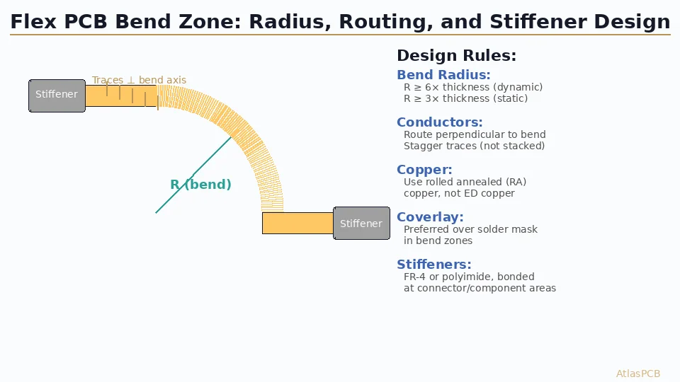
Flex PCB Design Guidelines: Bend Radius, Conductor Routing, Stiffeners, and Material Selection
Comprehensive design guidelines for flexible printed circuits (FPC) covering bend radius calculations, conductor routing rules, stiffener design, material selection, and reliability considerations for single-layer, double-layer, and multilayer flex circuits.
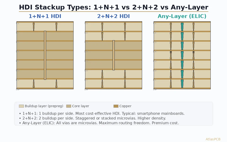
Advanced HDI PCB Stackup Design: Sequential Lamination, Any-Layer HDI, and ELIC
A deep technical guide to advanced HDI stackup architectures including sequential lamination, any-layer HDI, and Every Layer Interconnect (ELIC). Learn design rules, material selection, and manufacturing considerations for HDI Types I through III.
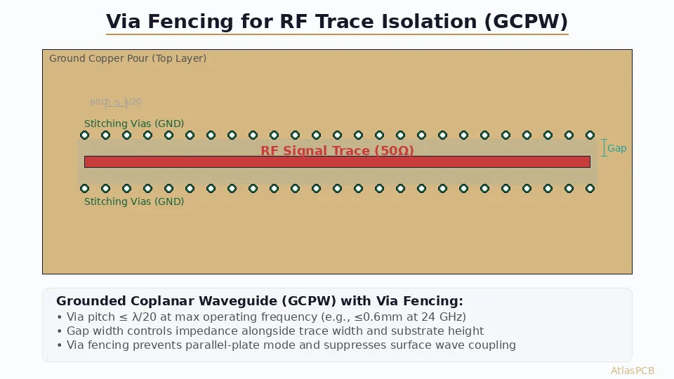
High-Frequency PCB Design Best Practices: RF/Microwave Layout, Ground Planes, Via Fencing, and Transition Design
Master RF and microwave PCB layout techniques including ground plane management, via fencing for isolation, coplanar waveguide transitions, and connector launch design. Covers frequencies from 1 GHz to 77 GHz.
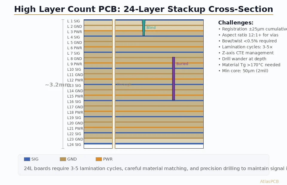
High Layer Count PCB Challenges: Designing and Manufacturing 20 to 68 Layer Boards
An in-depth analysis of the engineering challenges in high layer count PCB design and manufacturing—from registration accuracy and aspect ratio limits to thermal management, material selection, and cost optimization for 20 to 68 layer boards.
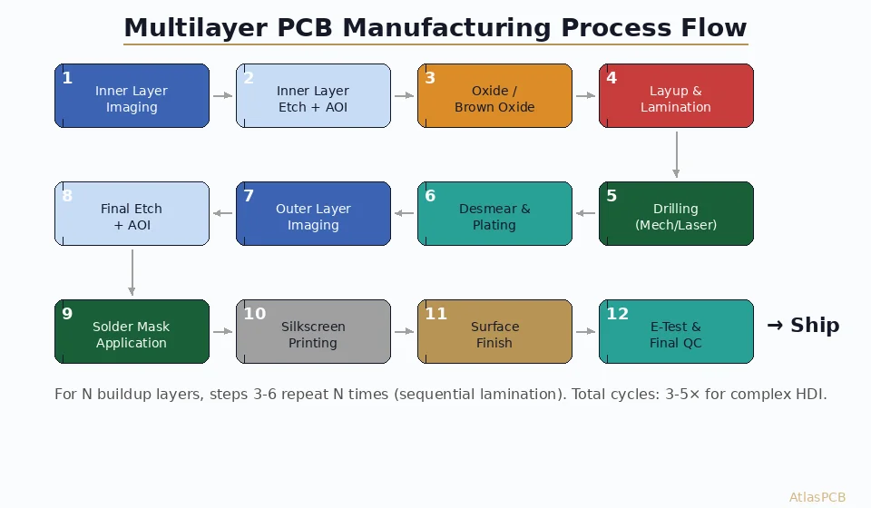
Multilayer PCB Manufacturing Process Explained: From 8-Layer to 40+ Layer Boards
A detailed walkthrough of the multilayer PCB manufacturing process for 8+ layer boards, covering inner layer imaging, lamination, drilling, plating, and the quality controls that ensure reliability at high layer counts.
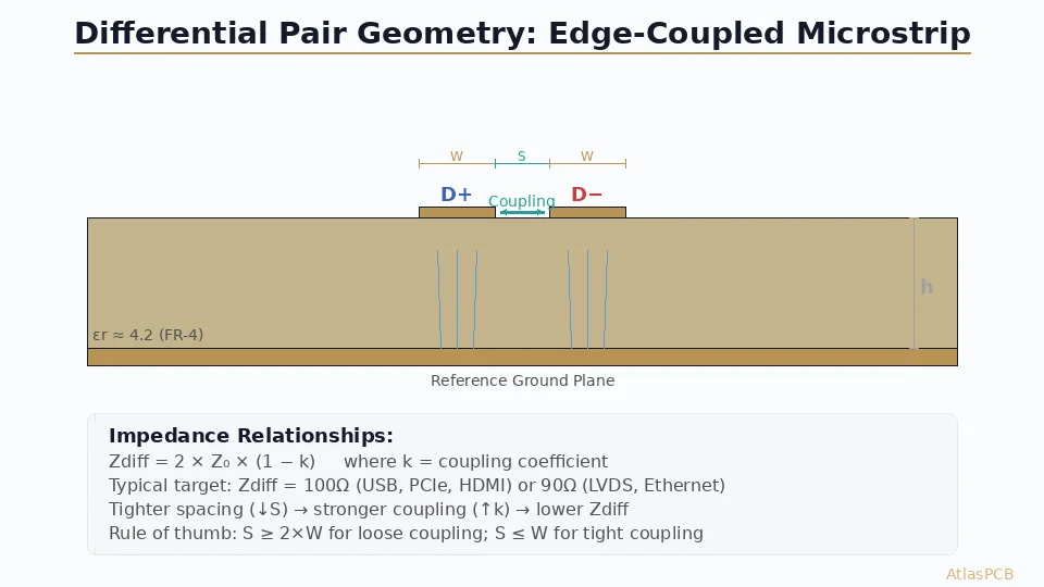
PCB Impedance Matching and Differential Pair Design: Spacing, Length Matching, and Layout
A comprehensive guide to differential pair PCB design covering impedance matching techniques, pair spacing optimization, length matching strategies, routing topologies, and practical design rules for high-speed serial interfaces including PCIe, USB4, and Ethernet.
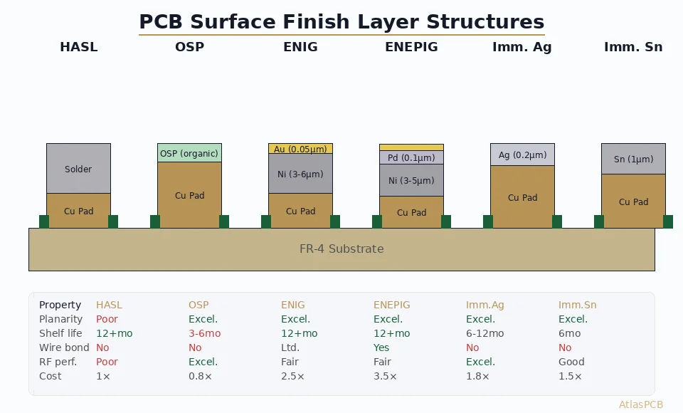
PCB Surface Finish Comparison 2026: HASL vs ENIG vs ENEPIG vs OSP vs Immersion Silver
A comprehensive 2026 comparison of PCB surface finishes—HASL, lead-free HASL, ENIG, ENEPIG, OSP, immersion silver, and immersion tin. Covers solderability, shelf life, cost, wire bonding compatibility, and application-specific recommendations.
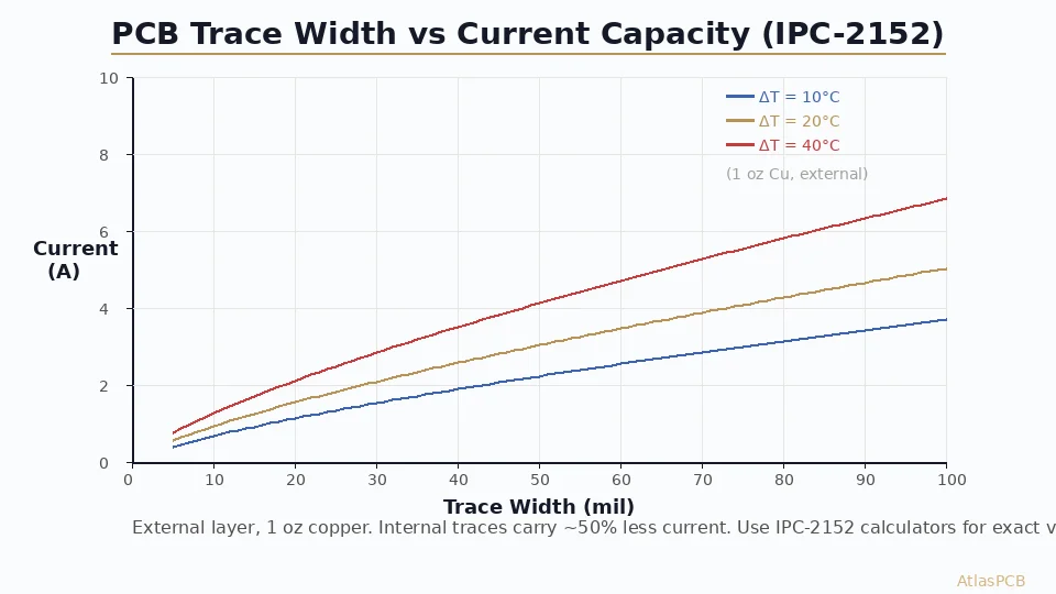
PCB Trace Width and Current Capacity: IPC-2152 Design Guide
A practical guide to PCB trace width sizing for current capacity using IPC-2152. Covers internal and external traces, temperature rise calculations, thermal relief design, and high-current PCB layout techniques for power delivery applications.
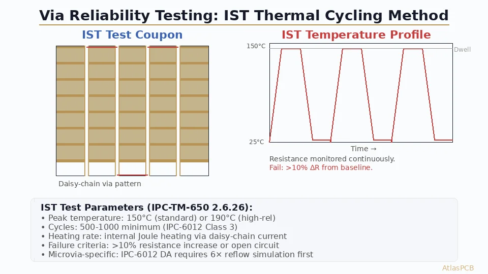
PCB Via Reliability Testing: IST, Thermal Cycling, and IPC-6012 Compliance for Microvias
A detailed guide to PCB via reliability testing methods including Interconnect Stress Testing (IST), thermal shock, thermal cycling, and microsection analysis. Covers microvia failure modes, IPC-6012 requirements, and best practices for qualifying via structures in HDI and high-reliability PCBs.
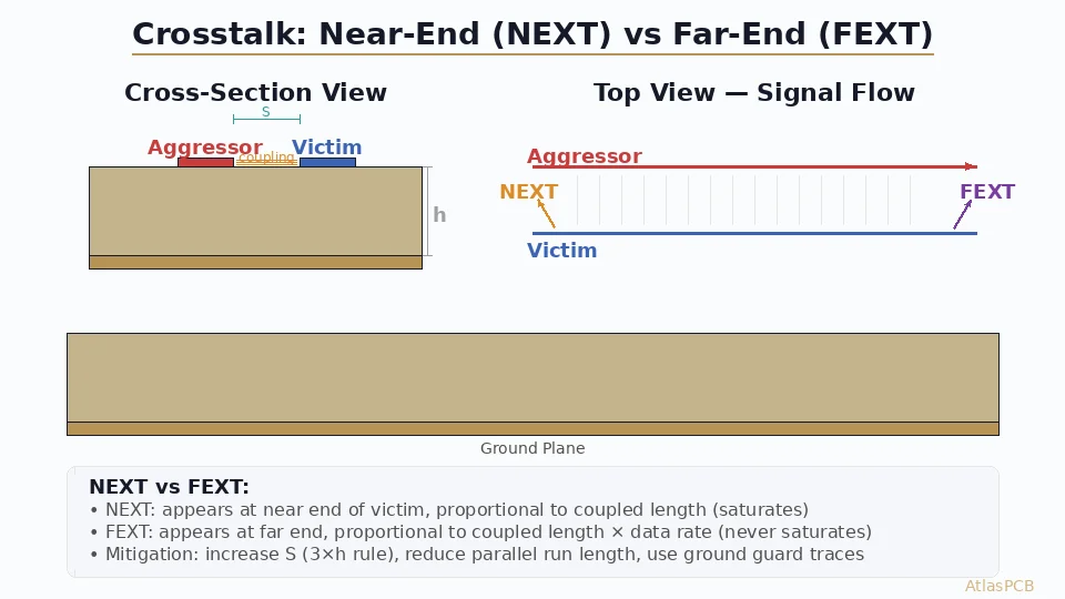
Signal Integrity in PCB Design: Impedance Control, Crosstalk, Via Stubs, and Return Paths
A comprehensive guide to signal integrity (SI) in PCB design covering impedance control, crosstalk mechanisms, via stub resonance, return path management, and practical design rules for high-speed digital and mixed-signal boards.
Differential Pair Routing: Rules, Impedance Control, and Layout Best Practices
A complete guide to differential pair routing on PCBs — covering impedance targets, trace geometry, length matching, via transitions, common mistakes, and stackup considerations for USB, PCIe, HDMI, and Ethernet designs.
PCB Sequential Lamination: Process, Design Rules, and When You Need It
A practical guide to PCB sequential lamination — what it is, how it works, when your board requires it, and the design rules that prevent costly manufacturing failures. Covers sub-composite planning, registration tolerance, material selection, and cost optimization.
BGA Escape Routing: Strategies for 0.4mm, 0.5mm, and 0.8mm Pitch
Practical guide to BGA escape routing for fine-pitch packages. Covers dog-bone fanout, via-in-pad, layer assignment strategies, and routing channel calculations for 0.4-1.0mm pitch BGAs on 4-12 layer PCBs.
ENEPIG vs ENIG: Which PCB Surface Finish for Your Design?
Detailed comparison of ENEPIG and ENIG surface finishes for PCB manufacturing. Covers layer structure, cost, wire bonding capability, signal integrity, and decision criteria for RF, BGA, and mixed-technology boards.
Heavy Copper PCB: Design Rules, Manufacturing Limits, and Thermal Management
Complete guide to heavy copper PCB design and manufacturing. Covers copper weight definitions, etching tolerances, thermal via design, current capacity, and specification best practices for power electronics.

Microstrip vs Stripline: Routing Strategies for Controlled Impedance PCBs
Engineering comparison of microstrip and stripline transmission line structures. Covers impedance behavior, loss characteristics, EMI performance, routing density, and when to use each topology in multilayer PCB design.
Rigid-Flex PCB Design: Stackup, Bend Rules, and Manufacturing Guidelines
Comprehensive guide to rigid-flex PCB design covering stackup construction, bend radius calculations, dynamic flex reliability, material selection, and IPC-2223 compliance for wearables, aerospace, and medical devices.
Controlled Impedance PCB: Design, Stackup & Testing Explained
Complete guide to controlled impedance PCB design. Covers impedance targets, stackup planning, trace geometry, dielectric selection, TDR testing, and manufacturing tolerances for single-ended and differential pairs.

PCB Back Drill: Why, When, and How to Specify It
Technical guide to PCB back drilling for high-speed signal integrity. Covers via stub effects, when back drilling is needed, depth control, design rules, and cost considerations for multi-gigabit applications.
Rogers 4003C Material Properties: Dk, Df, and Design Considerations
Complete technical reference for Rogers 4003C high-frequency laminate. Covers dielectric properties, thermal performance, processing compatibility, stackup design, and comparison with 4350B and FR4.
Taconic TLY-5 PCB: Properties, Applications, and Manufacturing Tips
Technical reference for Taconic TLY-5 PTFE-based RF laminate. Covers dielectric properties, processing requirements, stackup design, and practical comparison with Rogers alternatives for high-frequency PCB applications.
Via-in-Pad Design: Filled, Capped, and Plated Over — Complete Guide
Comprehensive guide to via-in-pad design for BGA escape routing and high-density PCBs. Covers filled and capped vias, copper plating, IPC standards, solder void prevention, and DFM considerations.
Blind Via vs Buried Via: Design Rules, Cost Impact & When to Use Each
A practical comparison of blind vias and buried vias for PCB design. Covers construction methods, aspect ratio limits, cost implications, reliability, and design decision criteria.
Complex PCB Manufacturer in China: HDI, RF & High-Reliability Boards
How to find and evaluate complex PCB manufacturers in China for HDI, RF, multilayer, and high-reliability boards. Covers factory qualification, communication, quality systems, and risk management.
HDI PCB Design Guide: Stackup Rules, Via Structures & DFM Checklist
A practical HDI PCB design guide covering microvia structures, stackup rules, BGA escape routing, via-in-pad design, copper fill requirements, and a complete DFM checklist for HDI boards.
HDI PCB Manufacturer: How to Choose the Right Partner for Complex Boards
A practical guide to evaluating HDI PCB manufacturers. Covers microvia capability, sequential lamination, laser drill specs, and what separates reliable suppliers from the rest.
High-Multilayer FR4 vs Standard FR4: When to Upgrade Material Grade
When your PCB needs high-Tg FR4 instead of standard. Covers Tg ratings, thermal performance, sequential lamination requirements, material grades, and cost impact for multilayer boards.
How to Order PCB from China: Complete Guide for Engineers
A practical guide to ordering PCBs from China — covering file preparation, manufacturer selection, communication, quality verification, shipping, and common pitfalls to avoid.
How to Design an HDI Stackup: Step-by-Step for First-Time Designers
A step-by-step guide to designing your first HDI PCB stackup. Covers HDI order selection, microvia planning, sub-lamination structure, impedance considerations, and common mistakes.
Impedance Controlled PCB Manufacturer: ±5% Guaranteed with TDR Testing
How to choose a PCB manufacturer for controlled impedance boards. Covers TDR testing, stackup simulation, tolerance verification, and what separates ±5% guaranteed from ±10% nominal.
IPC Class 3 Requirements: The Complete Guide for Designers
Everything PCB designers need to know about IPC Class 3 requirements — acceptability criteria, annular ring, plating thickness, cleanliness, testing, and when Class 3 is actually necessary.
IPC Class 2 vs Class 3: Which Standard Does Your Board Need?
A practical comparison of IPC-6012 Class 2 and Class 3 PCB requirements. Covers annular ring, plating thickness, testing, documentation, cost impact, and when each class is appropriate.
Military & Aerospace PCB Manufacturer: IPC Class 3, ITAR & Qualification Guide
How to evaluate PCB manufacturers for military, aerospace, and defense applications. Covers IPC Class 3, MIL-PRF-31032, AS9100, ITAR considerations, traceability requirements, and supplier qualification for defense and aerospace electronics.
Multilayer FR4 PCB Manufacturer: 8 to 68 Layers with Precision Alignment
How to choose a multilayer FR4 PCB manufacturer for 8-68 layer boards. Covers sequential lamination, impedance control, registration tolerance, and supplier evaluation criteria.
Multilayer PCB Stackup Design Guide: 8 to 30+ Layers Step by Step
A practical guide to designing multilayer PCB stackups from 8 to 30+ layers. Covers layer assignment, impedance planning, symmetry rules, material selection, and common mistakes.
PCB DFM Checklist: 50 Points to Review Before Sending Gerbers
A comprehensive DFM checklist for PCB designers. 50 verification points covering trace routing, via design, copper balance, stackup, solder mask, silkscreen, and fab notes — organized by category.
PCB Manufacturer with Engineering Review: Why Human DFM Audit Matters
Why automated DRC is not enough for complex PCBs. Learn what a human engineering review catches that software misses, and how to evaluate manufacturers on their pre-production review process.
PCB Manufacturing Process: 15 Steps from Gerber to Finished Board
A complete walkthrough of the PCB manufacturing process in 15 steps — from Gerber file input through inner layer imaging, lamination, drilling, plating, solder mask, surface finish, to electrical testing and final inspection.
PCB Material Selection Guide: FR4, Rogers, Polyimide & More
A comprehensive guide to PCB material selection. Covers FR4 grades, Rogers high-frequency laminates, polyimide flex materials, thermal properties, and selection criteria by application.
PCB Stackup Calculator: Layer Count, Material & Impedance Planning
A practical reference for PCB stackup planning. Includes standard stackup configurations for 4 to 24+ layers, impedance guidelines per layer type, material recommendations, and total thickness estimation.
RF PCB Design Guidelines: Layout, Grounding & Material Selection
Practical RF PCB design guidelines for engineers working above 1GHz. Covers transmission line design, grounding strategies, component placement, via fencing, material selection, and common RF layout mistakes.
RF PCB Manufacturer: What to Look For in a High-Frequency Board Supplier
How to evaluate RF PCB manufacturers for Rogers, Taconic, and Isola laminate boards. Covers material sourcing, impedance tolerance, mixed-dielectric capability, and supplier qualification.
RF PCB Materials Comparison: FR4 vs Rogers vs Taconic vs Isola
A comprehensive comparison of RF PCB materials — FR4, Rogers 4003C/4350B/5880, Taconic TLY-5, and Isola I-Tera MT40. Covers Dk, Df, thermal properties, processing, cost, and selection criteria.
Rogers 4350B vs FR4: When to Upgrade Your PCB Material
A head-to-head comparison of Rogers 4350B and FR4 for RF and high-speed applications. Covers Dk, Df, thermal performance, cost, and practical decision criteria for PCB engineers.
Rogers PCB Fabrication: Material Sourcing, Lead Times & Quality Control
What engineers need to know about Rogers PCB fabrication — material sourcing verification, processing requirements for thermoset vs PTFE, hybrid construction, quality control, and how to avoid common fabrication failures.
What Is DFM in PCB? Design for Manufacturability Explained
A clear explanation of DFM (Design for Manufacturability) in PCB design — what it covers, why it matters, and how it prevents costly manufacturing failures.

What Is a PCB? The Complete Beginner's Guide to Printed Circuit Boards
Learn the fundamentals of printed circuit boards (PCBs) - what they are, how they work, their basic structure, types, and applications across industries.

PCB Manufacturing Process: A Step-by-Step Guide from Design to Finished Board
Understand the complete PCB manufacturing process - from design file preparation through etching, drilling, plating, solder mask application, to final testing and quality control.

Single-Layer vs Multi-Layer PCB: How to Choose the Right Layer Count
Compare single-layer, double-layer, and multi-layer PCBs — understand the differences in cost, complexity, performance, and applications to choose the right layer count for your project.

PCB Surface Finish Guide: HASL, ENIG, OSP and More Compared
A comprehensive comparison of PCB surface finishes including HASL, lead-free HASL, ENIG, OSP, Immersion Silver, Immersion Tin, and ENEPIG — their pros, cons, costs, and best applications.

Rigid vs Flexible PCB: Materials, Applications, and How to Choose
Compare rigid, flexible, and rigid-flex PCBs — understand their materials, construction, bend radius, cost differences, and where each type excels in real-world applications.

PCB Design Rules: Trace Width, Spacing, and Via Size Guidelines
Master the essential PCB design rules — trace width for current capacity, minimum spacing for voltage isolation, via sizing standards, and design for manufacturability (DFM) best practices.

SMT vs Through-Hole Assembly: Which PCB Technology Is Right for You?
Compare Surface Mount Technology (SMT) and through-hole assembly — learn the differences in component types, soldering processes, mechanical strength, and when to use each approach.

PCB Copper Weight and Thickness Explained: From 0.5oz to Heavy Copper
Understand PCB copper weight — how oz/ft2 converts to thickness, current carrying capacity for different copper weights, heavy copper PCB applications, and thermal design considerations.

HDI PCB Technology: Microvias, Laser Drilling, and High-Density Design
Learn about HDI (High Density Interconnect) PCB technology — microvia types, laser drilling, buildup layer structures, HDI classifications, and applications in smartphones and 5G.

PCB Impedance Control: Why It Matters and How to Achieve It
Understand PCB impedance control — what impedance is, why it needs to be controlled, single-ended vs differential impedance, calculation methods, and testing with TDR.

PCB Thermal Management: Heat Dissipation Techniques for Reliable Electronics
Master PCB thermal management — understand heat sources, thermal vias, copper pours, thermal relief pads, metal-core PCBs, and simulation techniques for effective heat dissipation.

PCB Solder Mask: Types, Colors, and Functions Explained
Everything about PCB solder mask — LPI vs dry film types, color options (green, black, white, red, blue), dam design rules, solder mask opening strategies, and effects on assembly.

PCB Testing Methods: AOI, ICT, Flying Probe, and More
A complete guide to PCB testing methods — Automated Optical Inspection, In-Circuit Test, flying probe, functional testing, X-ray inspection, and when to use each approach.

Aluminum PCB for LED Applications: Design, Benefits, and Best Practices
Learn about aluminum metal core PCBs (MCPCB) for LED lighting — structure, thermal conductivity, dielectric layer selection, design guidelines, and comparison with FR-4 boards.
PCB Panelization: V-Cut vs Tab Routing Guide
Learn PCB panelization methods — V-scoring, tab routing with mouse bites, panel size optimization, fiducials, tooling holes, and depanelization best practices.
PCB Via Types: Through-Hole, Blind, Buried, and Microvias Explained
Understand all PCB via types — through-hole, blind, buried, microvia, and via-in-pad. Learn their construction, aspect ratios, cost implications, and when to use each type.
PCB Gerber Files: What They Are and How to Generate Them
Understand PCB Gerber files — the RS-274X format, ODB++, which layers to include, how to generate them from KiCad, Altium, and Eagle, and common mistakes to avoid.
IPC Standards for PCB: Understanding Class 1, 2, and 3 Requirements
Learn about IPC standards for PCB quality — IPC-A-600, IPC-6012, and the three performance classes. Understand acceptance criteria for annular ring, hole quality, conductor width, and more.
PCB Stackup Design: Best Practices for Signal Integrity and EMI Control
Master PCB stackup design — understand symmetric construction, signal-ground pairing, common 4/6/8-layer stackups, material selection, impedance impact, and EMI reduction strategies.
Common PCB Defects and How to Prevent Them
Identify and prevent the most common PCB defects — solder bridges, tombstoning, cold joints, delamination, copper cracking, CAF, via failures, and DFM best practices for defect-free boards.
PCB Materials Guide: FR-4, CEM, Rogers, and Polyimide Compared
Compare common PCB substrate materials — FR-4, CEM-1, CEM-3, Rogers, polyimide, and ceramic. Understand their properties, costs, and best applications for your design.
PCB Prototyping vs Mass Production: Key Differences and Best Practices
Understand the differences between PCB prototyping and mass production — cost structures, lead times, testing strategies, design considerations, and how to transition smoothly from prototype to volume.
PCBA Assembly Process: From Bare Board to Finished Product
Understand the complete PCB assembly (PCBA) process — solder paste printing, pick and place, reflow soldering, wave soldering, inspection, and functional testing explained step by step.
BGA Soldering and Rework: Challenges, Inspection, and Best Practices
Master BGA technology — understand Ball Grid Array soldering challenges, X-ray inspection techniques, common defects (voiding, head-in-pillow, bridging), and professional rework procedures.
High-Speed PCB Design: Signal Integrity Essentials for Modern Electronics
Master high-speed PCB design — transmission line theory, return paths, crosstalk, power delivery network, and practical guidelines for DDR, PCIe, USB, and Ethernet routing.
RF and Microwave PCB Design: Materials, Layout, and Manufacturing Guide
Learn RF/microwave PCB design essentials — material selection, transmission line structures, grounding techniques, component placement, and manufacturing considerations for 1-40+ GHz circuits.

High-Frequency Microwave PCB Substrate Selection: Dk & Df Comparison of PTFE, Ceramic-Filled, and FR-4
As 5G, automotive radar, and satellite communications demand ever-higher signal integrity, choosing the right PCB substrate is critical. This guide compares the dielectric constant (Dk) and dissipation factor (Df) of FR-4, PTFE, and ceramic-filled substrates for high-frequency microwave circuits.
PCB Grounding Techniques: Star, Split, and Solid Ground Plane Strategies
Master PCB grounding — understand solid ground planes, star grounding, split planes, analog-digital ground separation, and best practices for noise-free circuit operation.
EMC/EMI Design for PCBs: Passing Compliance on the First Try
Practical EMC/EMI design techniques for PCBs — understand radiated and conducted emissions, filtering, shielding, grounding, and layout strategies to pass FCC, CE, and CISPR compliance testing.
PCB Trace Antenna Design: WiFi, Bluetooth, NFC, and LoRa Antenna Guide
Design PCB trace antennas for wireless applications — inverted-F, meander line, and loop antenna structures for WiFi, Bluetooth, NFC, LoRa, and cellular IoT with layout and tuning guidelines.
Automotive PCB Requirements: Standards, Materials, and Reliability for Vehicle Electronics
Understand automotive PCB requirements — AEC-Q standards, IATF 16949, temperature grades, material selection, reliability testing, and design considerations for automotive-grade circuit boards.
Medical Device PCB Standards: IEC 60601, FDA, and Reliability Requirements
Navigate medical device PCB requirements — IEC 60601 safety standards, FDA regulations, biocompatibility, creepage/clearance rules, and reliability considerations for medical electronics.
PCB Cost Optimization: 15 Practical Ways to Reduce Board Cost
Reduce PCB costs without sacrificing quality — practical tips for layer count reduction, panel optimization, material selection, design simplification, and volume pricing strategies.
Conformal Coating for PCBs: Types, Application Methods, and Selection Guide
Protect your PCBs with conformal coating — compare acrylic, silicone, urethane, epoxy, and parylene coatings. Learn application methods, thickness requirements, and selection criteria.
PCB Reliability Testing: HALT, HASS, Thermal Cycling, and Life Testing
Ensure product reliability with PCB testing methods — HALT (Highly Accelerated Life Testing), HASS, thermal cycling, vibration testing, and accelerated aging for predicting product lifespan.
PCB Design Software Comparison: KiCad vs Altium vs Eagle vs OrCAD
Compare the top PCB design tools — KiCad, Altium Designer, Eagle, and OrCAD. Understand features, pricing, learning curve, and which tool fits your project needs.
High-Voltage PCB Design: Creepage, Clearance, and Safety Isolation
Design safe high-voltage PCBs — understand creepage and clearance requirements, IEC standards, slot and cutout techniques, material selection, and safety certification for mains-powered electronics.
PCB Pad Design for BGA, QFN, and Passive Components: Best Practices
Optimize PCB pad design for reliable soldering — BGA pad strategies, QFN thermal pad design, passive component pad geometry for anti-tombstoning, and IPC-7351 land pattern standards.
PCB Environmental Standards: RoHS, REACH, UL, and Halogen-Free Compliance
Navigate PCB environmental and safety regulations — RoHS restricted substances, REACH SVHC compliance, UL flammability certification, halogen-free requirements, and WEEE directives.