· AtlasPCB Engineering · Engineering · 7 min read
PCB Stackup Calculator: Layer Count, Material & Impedance Planning
A practical reference for PCB stackup planning. Includes standard stackup configurations for 4 to 24+ layers, impedance guidelines per layer type, material recommendations, and total thickness estimation.
Planning a PCB stackup before routing saves time and prevents costly re-spins. This guide provides reference stackup configurations, impedance planning data, and thickness estimation tools for 4 to 24+ layer designs.
For a deeper discussion of stackup design principles, see our [multilayer PCB stackup design guide]/blog/multilayer-pcb-stackup-design-guide/).
Quick Reference: Standard Stackup Configurations
4-Layer Stackup (1.0-1.6mm)
L1 — Signal/Component (1oz)
    ─── prepreg: 2×1080 (7.8 mil) ───
L2 — Ground (1oz)
    ─── core: 30-40 mil ───
L3 — Power (1oz)
    ─── prepreg: 2×1080 (7.8 mil) ───
L4 — Signal/Component (1oz)
Total thickness: ~1.57mm (62 mil) with 40 mil core
Impedance reference:
| Trace Type | Target | Trace Width | Dielectric |
|---|---|---|---|
| 50Ω SE microstrip (L1/L4) | 50Ω | ~7.2 mil | 7.8 mil prepreg |
| 100Ω diff microstrip (L1/L4) | 100Ω | 5/5 mil, 6 mil gap | 7.8 mil prepreg |
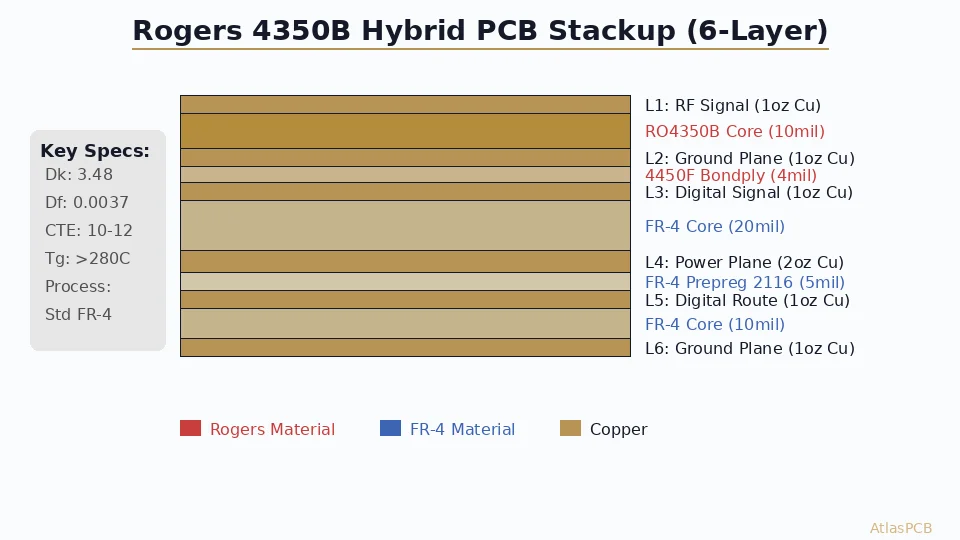
6-Layer Stackup (1.6mm)
L1 — Signal (1oz)
    ─── prepreg: 1×7628 (7.0 mil) ───
L2 — Ground (1oz)
    ─── core: 8 mil ───
L3 — Signal (0.5oz)
    ─── prepreg: 1×2116 (4.5 mil) ───
L4 — Power (1oz)
    ─── core: 8 mil ───
L5 — Ground (1oz)
    ─── prepreg: 1×7628 (7.0 mil) ───
L6 — Signal (1oz)
Total thickness: ~1.60mm (63 mil)
Impedance reference:
| Trace Type | Target | Layer | Trace Width | Dielectric |
|---|---|---|---|---|
| 50Ω SE microstrip | 50Ω | L1/L6 | ~6.5 mil | 7.0 mil |
| 50Ω SE stripline | 50Ω | L3 | ~4.0 mil | 4.5 mil to L2 |
| 100Ω diff stripline | 100Ω | L3 | 3.5/3.5, 6 mil gap | 4.5 mil |
8-Layer Stackup (1.6mm)
L1 — Signal (1oz)
    ─── prepreg: 1×2116 (4.5 mil) ───
L2 — Ground (1oz)
    ─── core: 6 mil ───
L3 — Signal (0.5oz)
    ─── prepreg: 1×1080 (3.9 mil) ───
L4 — Power (1oz)
    ─── prepreg: 1×1080 (3.9 mil) ───
L5 — Ground (1oz)
    ─── core: 6 mil ───
L6 — Signal (0.5oz)
    ─── prepreg: 1×2116 (4.5 mil) ───
L7 — Ground (1oz)
    ─── core: 6 mil ───
L8 — Signal (1oz)
Total thickness: ~1.60mm (63 mil)
Notes: L4-L5 is a tightly coupled power-ground pair (3.9 mil) for distributed decoupling. Every signal layer (L1, L3, L6, L8) has an adjacent ground or power reference.
10-Layer Stackup (2.0mm)
L1  — Signal (1oz)
     ─── prepreg: 1×2116 (4.5 mil) ───
L2  — Ground (1oz)
     ─── core: 6 mil ───
L3  — Signal (0.5oz)
     ─── prepreg: 1×1080 (3.9 mil) ───
L4  — Power VCC (1oz)
     ─── prepreg: 1×1080 (3.9 mil) ───
L5  — Ground (1oz)
     ─── core: 4 mil ───
L6  — Power 3.3V (1oz)
     ─── prepreg: 1×1080 (3.9 mil) ───
L7  — Ground (1oz)
     ─── prepreg: 1×1080 (3.9 mil) ───
L8  — Signal (0.5oz)
     ─── core: 6 mil ───
L9  — Ground (1oz)
     ─── prepreg: 1×2116 (4.5 mil) ───
L10 — Signal (1oz)
Total thickness: ~2.0mm (79 mil)
12-Layer Stackup (2.0mm)
L1  — Signal (1oz)
     ─── prepreg: 1×2116 (4.5 mil) ───
L2  — Ground (1oz)
     ─── core: 4 mil ───
L3  — Signal (0.5oz)
     ─── prepreg: 1×1080 (3.5 mil) ───
L4  — Ground (1oz)
     ─── prepreg: 1×1080 (3.0 mil) ───
L5  — Power VCC (1oz)
     ─── prepreg: 1×1080 (3.0 mil) ───
L6  — Signal (0.5oz)
     ─── core: 4 mil ───
L7  — Signal (0.5oz)
     ─── prepreg: 1×1080 (3.0 mil) ───
L8  — Power 3.3V (1oz)
     ─── prepreg: 1×1080 (3.0 mil) ───
L9  — Ground (1oz)
     ─── prepreg: 1×1080 (3.5 mil) ───
L10 — Signal (0.5oz)
     ─── core: 4 mil ───
L11 — Ground (1oz)
     ─── prepreg: 1×2116 (4.5 mil) ───
L12 — Signal (1oz)
Total thickness: ~2.0mm (79 mil)

Thickness Estimation Quick Reference
Copper Layer Thickness
| Weight | Thickness |
|---|---|
| 0.5 oz | 0.7 mil (18μm) |
| 1 oz | 1.4 mil (35μm) |
| 2 oz | 2.8 mil (70μm) |
| 3 oz | 4.2 mil (105μm) |
Common Prepreg Options
| Style | Thickness (mil) | Dk @1GHz | Glass/Resin |
|---|---|---|---|
| 106 | 2.0 | 3.8-4.0 | High resin |
| 1080 | 3.0-3.9 | 4.0-4.2 | Medium resin |
| 2116 | 4.0-4.8 | 4.2-4.4 | Standard |
| 7628 | 6.5-7.5 | 4.4-4.7 | Low resin |
Note: Dk varies with resin content. High-resin prepregs (106, 1080) have lower Dk; low-resin prepregs (7628) have higher Dk due to glass content. This affects impedance calculations.
Typical Total Board Thickness
| Layer Count | Standard Thickness | Thin Option | Thick Option |
|---|---|---|---|
| 2-layer | 1.0mm / 1.6mm | 0.4mm | 2.0mm |
| 4-layer | 1.0mm / 1.6mm | 0.6mm | 2.0mm |
| 6-layer | 1.6mm | 1.0mm | 2.0mm |
| 8-layer | 1.6mm | 1.2mm | 2.4mm |
| 10-layer | 2.0mm | 1.6mm | 2.4mm |
| 12-layer | 2.0mm | 1.6mm | 2.8mm |
| 16-layer | 2.4mm | 2.0mm | 3.2mm |
| 20-layer | 3.0mm | 2.4mm | 4.0mm |
| 24-layer | 3.6mm | 3.0mm | 4.8mm |
Impedance Quick Reference
Approximate trace widths for common impedance targets on FR4 (Dk ≈ 4.2, 1oz copper). These are estimates — use your manufacturer’s field solver for production values.
Single-Ended Microstrip (Outer Layer)
| Target | Dielectric Height | Trace Width (approx.) |
|---|---|---|
| 50Ω | 3.5 mil | 5.3 mil |
| 50Ω | 4.5 mil | 7.0 mil |
| 50Ω | 7.0 mil | 11.5 mil |
| 75Ω | 4.5 mil | 3.5 mil |
Single-Ended Stripline (Inner Layer)
| Target | Dielectric Height (each side) | Trace Width (approx.) |
|---|---|---|
| 50Ω | 3.5 mil | 4.2 mil |
| 50Ω | 4.5 mil | 5.8 mil |
| 50Ω | 6.0 mil | 8.0 mil |
Differential Microstrip (Outer Layer)
| Target | Dielectric Height | Trace/Space (approx.) |
|---|---|---|
| 85Ω | 4.5 mil | 4.0 / 5.0 mil |
| 90Ω | 4.5 mil | 3.8 / 6.0 mil |
| 100Ω | 4.5 mil | 3.5 / 8.0 mil |
| 100Ω | 7.0 mil | 5.0 / 7.0 mil |
Differential Stripline (Inner Layer)
| Target | Dielectric Height | Trace/Space (approx.) |
|---|---|---|
| 85Ω | 3.5 mil | 3.5 / 5.0 mil |
| 100Ω | 3.5 mil | 3.0 / 7.0 mil |
| 100Ω | 4.5 mil | 4.0 / 7.0 mil |
Via Aspect Ratio Calculator
Before finalizing your stackup, verify that your vias are manufacturable:
Aspect ratio = Board thickness ÷ Drill diameter
| Board Thickness | 0.20mm Drill | 0.25mm Drill | 0.30mm Drill | 0.35mm Drill |
|---|---|---|---|---|
| 1.0mm | 5:1 ✅ | 4:1 ✅ | 3.3:1 ✅ | 2.9:1 ✅ |
| 1.6mm | 8:1 ✅ | 6.4:1 ✅ | 5.3:1 ✅ | 4.6:1 ✅ |
| 2.0mm | 10:1 ⚠️ | 8:1 ✅ | 6.7:1 ✅ | 5.7:1 ✅ |
| 2.4mm | 12:1 ❌ | 9.6:1 ⚠️ | 8:1 ✅ | 6.9:1 ✅ |
| 3.0mm | 15:1 ❌ | 12:1 ❌ | 10:1 ⚠️ | 8.6:1 ✅ |
✅ Standard capability (≤8:1) | ⚠️ Advanced (8-10:1, verify with manufacturer) | ❌ Beyond standard (>10:1, requires specialty process or blind/buried vias)
Material Selection Quick Guide
| Application | Recommended Material | Dk @1GHz | Df @1GHz |
|---|---|---|---|
| General (≤1GHz) | Standard FR4, mid-Tg | 4.3-4.5 | 0.020 |
| Industrial (≤1GHz, 10+ layers) | High-Tg FR4 | 4.2-4.4 | 0.018 |
| High-speed digital (10-25Gbps) | Low-loss FR4 (Megtron 4) | 3.8 | 0.005 |
| High-speed digital (25Gbps+) | Very-low-loss (Megtron 6) | 3.7 | 0.002 |
| RF 1-10GHz | Rogers 4003C / 4350B | 3.38-3.48 | 0.003-0.004 |
| RF 10GHz+ | Rogers 5880 / Taconic TLY-5 | 2.20 | 0.001 |
| Flex circuits | Polyimide (Kapton) | 3.4 | 0.003 |
| High power / LED | Aluminum MCPCB | N/A | N/A |
How to Use This Data
- Start with layer count — estimate based on net count and complexity
- Select a reference stackup from the configurations above
- Check impedance — use the quick reference tables to estimate trace widths
- Verify aspect ratio — ensure your vias work with the total thickness
- Send to manufacturer — have them run the field solver and confirm or adjust trace widths
Do not route based on these approximate values. They are starting points for planning. Your manufacturer must simulate impedance on the actual materials they will use, accounting for manufacturing tolerances, etch factor, and solder mask effects.
Free Stackup Planning from Atlas PCB
Atlas PCB provides stackup planning and impedance simulation as part of every order:
- Pre-routing consultation — send us your layer count, impedance targets, and thickness constraints before you route
- Field solver simulation — Polar SI with material-specific Dk data for precise trace width recommendations
- Material mapping — your specified dielectrics matched to available prepreg and core from current stock
- Via feasibility check — aspect ratios verified against factory capability
- Updated stackup document — returned to you with recommended trace widths per layer before routing begins
This service is included at no additional cost. It prevents the costly cycle of routing, sending to fab, discovering impedance does not work, re-stacking, and re-routing.
Frequently Asked Questions
How do I calculate PCB stackup thickness?
Add all copper layer thicknesses (1oz = 35μm per layer) plus all dielectric thicknesses (prepreg and core). For example, an 8-layer board with 1oz copper, two 6mil cores, and five 3.5-4.5mil prepreg layers totals approximately 1.6mm. Actual thickness varies ±5-10% from calculation due to resin flow during lamination — your manufacturer provides the final confirmed thickness after stackup simulation.
What is the standard PCB thickness?
1.6mm (63 mil) is the most common standard, suitable for 4-8 layer boards. Other standards: 0.8mm (thin), 1.0mm (compact), 2.0mm (10-14 layers), 2.4mm (14-20 layers). Board thickness directly affects via aspect ratio — thicker boards need larger drills or blind/buried vias to maintain reliable plating.
How do I choose dielectric thickness for impedance control?
Target trace widths that your design can accommodate, then select dielectric thickness to produce the target impedance at that trace width. For 50Ω microstrip on FR4: 3.5 mil dielectric gives ~5.3 mil traces (tight routing), 4.5 mil gives ~7.0 mil traces (comfortable routing). Start with the quick reference tables in this guide, then have your manufacturer confirm with a field solver before routing.
Summary
- Use reference stackups as starting points — always verify with your manufacturer’s field solver
- Standard 1.6mm thickness fits 4-8 layers; thicker boards for higher layer counts
- Every signal layer needs an adjacent reference plane
- Check via aspect ratio against board thickness before committing to a drill size
- Approximate impedance values are for planning only — production requires field solver simulation
Need help planning your stackup? Upload your Gerbers for a free engineering review with stackup simulation, or send us your requirements before routing and we will recommend an optimal configuration.
Related guides: [Multilayer PCB Stackup Design Guide]/blog/multilayer-pcb-stackup-design-guide/) | [PCB Impedance Control]/blog/pcb-impedance-control/) | [PCB Material Selection Guide]/blog/pcb-material-selection-guide/)
Further Reading
[Rogers 4003C Material Properties: Dk, Df, and Design Considerations]/blog/rogers-4003c-properties/)
[Taconic TLY-5 PCB: Properties, Applications, and Manufacturing Tips]/blog/taconic-tly-5-pcb/)
[High-Multilayer FR4 vs Standard FR4: When to Upgrade Material Grade]/blog/high-multilayer-fr4-vs-standard-fr4/)
[PCB Manufacturer with Engineering Review: Why Human DFM Audit Matters]/blog/pcb-manufacturer-engineering-review/)
[PCB Solder Mask: Types, Colors, and Functions Explained]/blog/pcb-solder-mask-guide/)
[HDI PCB Design Guide: Stackup Rules, Via Structures & DFM Checklist]/blog/hdi-pcb-design-guide/)
[PCB DFM Checklist: 50 Points to Review Before Sending Gerbers]/blog/pcb-dfm-checklist/)
About AtlasPCB — We specialize in complex PCB manufacturing for HDI, RF, and high-reliability applications. Explore our impedance-controlled PCB manufacturing . Every order includes free engineering review. Get your quote.
Reviewed by AtlasPCB Engineering Team — IPC-certified manufacturing specialists with 15+ years of production experience in HDI, RF, and high-reliability PCB fabrication. Content based on factory floor data and real customer design reviews.
- pcb stackup
- layer count
- impedance calculator
- stackup planning
- pcb design tool