· AtlasPCB Engineering · Engineering · 12 min read
Multilayer PCB Stackup Design Guide: 8 to 30+ Layers Step by Step
A practical guide to designing multilayer PCB stackups from 8 to 30+ layers. Covers layer assignment, impedance planning, symmetry rules, material selection, and common mistakes.
Stackup design is where the electrical and mechanical requirements of your PCB meet the physical reality of manufacturing. A well-designed stackup controls impedance, minimizes crosstalk, manages power delivery, and survives the lamination press without warping. A poor stackup creates problems that no amount of routing optimization can fix.
This guide walks through the practical process of designing multilayer stackups from 8 to 30+ layers, with rules, examples, and the most common mistakes.
The Fundamental Rules
Before diving into specific layer counts, these rules apply to every multilayer stackup:
Rule 1: Every Signal Layer Needs a Reference Plane
A high-speed signal trace is one half of a transmission line. The reference plane (ground or power) is the other half. Without an adjacent reference plane, you do not have a transmission line — you have an antenna.
Practical implication: For every signal layer in your stackup, plan a ground or power plane on at least one adjacent layer. Two signal layers stacked together without a reference plane between them create broadside coupling (crosstalk) and uncontrolled impedance.
Rule 2: Symmetry Around the Center
The stackup must be symmetric about the board’s center axis — same dielectric thickness, same copper weight, same layer type mirrored above and below center.
Symmetric:                    Asymmetric (bad):
L1 — Signal (1oz)            L1 — Signal (2oz)
L2 — Ground (1oz)            L2 — Ground (1oz)
L3 — Signal (0.5oz)          L3 — Signal (0.5oz)
    --- center ---                --- center ---
L4 — Signal (0.5oz)          L4 — Power (1oz)
L5 — Ground (1oz)            L5 — Signal (0.5oz)
L6 — Signal (1oz)            L6 — Signal (1oz)
The symmetric stackup has balanced copper distribution and will lie flat after lamination. The asymmetric one will warp.
Rule 3: Keep High-Speed Signals on Inner Layers
Surface layers (L1, bottom layer) are exposed to:
- Solder mask thickness variation (affects microstrip impedance)
- Etch factor variation (outer layers etch differently than inner)
- Environmental effects (moisture, contamination)
Where possible, route the most impedance-critical signals on inner stripline layers adjacent to ground planes. Use outer layers for component connections, short fan-out traces, and non-critical routing.
Rule 4: Pair Power and Ground Planes Closely
Tightly coupled power-ground plane pairs (2-4 mil dielectric) provide:
- Distributed decoupling capacitance across the entire board
- Low-impedance power delivery
- Reduced EMI radiation from power switching
Place at least one power-ground pair with thin dielectric in every stackup.
Rule 5: Match Available Materials
Your stackup design must use dielectric thicknesses that actually exist as standard prepreg and core materials. Specifying a 3.2 mil dielectric when the manufacturer’s closest option is 3.5 mil or 2.8 mil forces a compromise.
Common available thicknesses:
- Cores: 2, 3, 4, 5, 6, 8, 10, 12, 14, 20, 30, 40, 60 mil
- Prepreg (single ply): 2.0, 2.7, 3.5, 4.5, 5.5, 7.0 mil (varies by style)
- Prepreg (double ply): 5-8 mil (two sheets combined)
Always coordinate stackup design with your manufacturer — they know which specific materials are in stock and can propose alternatives if your target thickness is not available.
Layer Assignment Strategy
What Goes Where
| Layer Type | Placement Priority | Notes |
|---|---|---|
| Ground plane | Adjacent to every signal layer | Primary reference for impedance and return current |
| High-speed signal | Inner stripline layers | Best impedance control, shielded from external noise |
| Power plane | Paired with ground (thin dielectric) | Distributed decoupling, power delivery |
| Low-speed signal | Outer microstrip layers | Less critical, use for component fan-out |
| Clock signals | Inner layer with dedicated ground ref | Minimize radiation, control impedance tightly |
8-Layer Stackup Examples
Example A: 4 signal + 2 ground + 2 power
L1 — Signal (microstrip)
    ─── prepreg 4 mil ───
L2 — Ground
    ─── core 8 mil ───
L3 — Signal (stripline)
    ─── prepreg 4 mil ───
L4 — Power
    ─── prepreg 4 mil ───
L5 — Ground
    ─── core 8 mil ───
L6 — Signal (stripline)
    ─── prepreg 4 mil ───
L7 — Power/Ground
    ─── core 8 mil ───
L8 — Signal (microstrip)
Pros: 4 signal layers, all with adjacent reference planes. L4-L5 power-ground pair provides distributed decoupling.
Cons: Only 4 routing layers. L3 and L6 are single-stripline (reference plane on one side only for impedance calculation).
Example B: 4 signal + 4 planes (high integrity)
L1 — Signal (microstrip)
    ─── prepreg 4 mil ───
L2 — Ground
    ─── core 10 mil ───
L3 — Signal (dual stripline)
    ─── prepreg 3.5 mil ───
L4 — Power
    ─── prepreg 3.5 mil ───
L5 — Ground
    ─── prepreg 3.5 mil ───
L6 — Signal (dual stripline)
    ─── core 10 mil ───
L7 — Ground
    ─── prepreg 4 mil ───
L8 — Signal (microstrip)
Pros: Every signal layer has ground reference on at least one side. L4-L5 is tightly coupled power-ground pair. L3 and L6 are between two planes (dual stripline) for maximum shielding.
Cons: Only 4 routing layers. Higher total thickness due to extra planes.
12-Layer Stackup Example
L1  — Signal (microstrip)
     ─── prepreg 3.5 mil ───
L2  — Ground
     ─── core 6 mil ───
L3  — Signal (stripline)
     ─── prepreg 3.5 mil ───
L4  — Ground
     ─── prepreg 3 mil ───
L5  — Power (VCC)
     ─── prepreg 3 mil ───
L6  — Signal (stripline)
     ─── core 6 mil ───
L7  — Signal (stripline)
     ─── prepreg 3 mil ───
L8  — Power (3.3V)
     ─── prepreg 3 mil ───
L9  — Ground
     ─── prepreg 3.5 mil ───
L10 — Signal (stripline)
     ─── core 6 mil ───
L11 — Ground
     ─── prepreg 3.5 mil ───
L12 — Signal (microstrip)
Layer assignment rationale:
- L1/L12: Component-side routing (microstrip, less critical signals)
- L3/L10: High-speed signals (stripline between two planes)
- L6/L7: Additional routing (stripline, reference planes above/below)
- L2/L4/L9/L11: Ground planes (provides reference for every signal layer)
- L5/L8: Power planes (paired with adjacent ground for decoupling)
- L4-L5 and L8-L9: Tightly coupled plane pairs (3 mil dielectric)
16+ Layer Stackup Principles
Above 16 layers, the same principles scale:
- Start with the plane structure — place ground and power planes first
- Insert signal layers between planes, ensuring every signal layer has at least one adjacent reference
- Place tightly-coupled power-ground pairs (2-3 mil) for each major power rail
- Check symmetry after each layer addition
- Verify total thickness is within target and aspect ratio limits for vias
For 20+ layer boards: Consider dedicating separate ground planes for different circuit sections (analog ground, digital ground, RF ground) to minimize noise coupling through shared return paths. These grounds should be connected at a single point near the power entry.

Impedance Planning in Stackup Design
Process
- List all impedance targets — 50Ω single-ended, 100Ω differential, 75Ω, etc.
- Assign each impedance target to a specific layer — know which layers carry which impedance
- Calculate trace width for each target using the actual dielectric thickness and Dk of the material on that layer
- Verify that trace width is routable — if impedance requires a 2 mil trace and your minimum is 4 mil, change the dielectric thickness or layer assignment
- Coordinate with manufacturer — they run the field solver and confirm or adjust
Common Impedance Configurations
| Type | Target | Typical Layer Position | Trace Width (approx.) |
|---|---|---|---|
| 50Ω single-ended microstrip | 50Ω | Outer layer (L1/LN) | 4-6 mil on 3.5 mil prepreg |
| 50Ω single-ended stripline | 50Ω | Inner layer | 3-5 mil on 4 mil dielectric |
| 100Ω differential microstrip | 100Ω | Outer layer | 4/4 mil traces, 5 mil gap |
| 100Ω differential stripline | 100Ω | Inner layer | 3.5/3.5 mil traces, 5 mil gap |
| 85Ω differential (USB 3.0) | 85Ω | Inner or outer | Varies by dielectric |
| 90Ω differential (USB 2.0) | 90Ω | Any | Varies by dielectric |
Trace widths are approximate and depend on specific material Dk, copper weight, and solder mask presence.
The Dielectric Thickness vs. Trace Width Trade-off
For a fixed impedance target:
- Thinner dielectric → narrower trace (harder to route, more sensitive to etch variation)
- Thicker dielectric → wider trace (easier to route, consumes more space, increases layer-to-layer distance)
Choose the dielectric thickness that gives a trace width your design can accommodate. If your routing is dense with 3 mil traces, use thinner dielectrics. If you have space, use thicker dielectrics for more manufacturing margin.
Material Selection for the Stackup
Standard FR4
Adequate for most applications below 3GHz. Choose the appropriate Tg rating:
| Layer Count | Recommended Tg | Reason |
|---|---|---|
| 4-8 layers | ≥150°C (mid-Tg) | Survives lead-free reflow with margin |
| 10-16 layers | ≥170°C (high-Tg) | Multiple lamination cycles + reflow |
| 18+ layers | ≥170°C (high-Tg) | Mandatory for sequential lamination reliability |
Low-Loss FR4 Alternatives
For high-speed digital (10Gbps+ NRZ, 25Gbps+ PAM4) where standard FR4 loss is too high:
- Panasonic Megtron 4 — Df 0.005 at 1GHz, FR4-compatible processing
- Isola I-Speed — Df 0.005, good availability
- Panasonic Megtron 6 — Df 0.002 at 1GHz, premium pricing
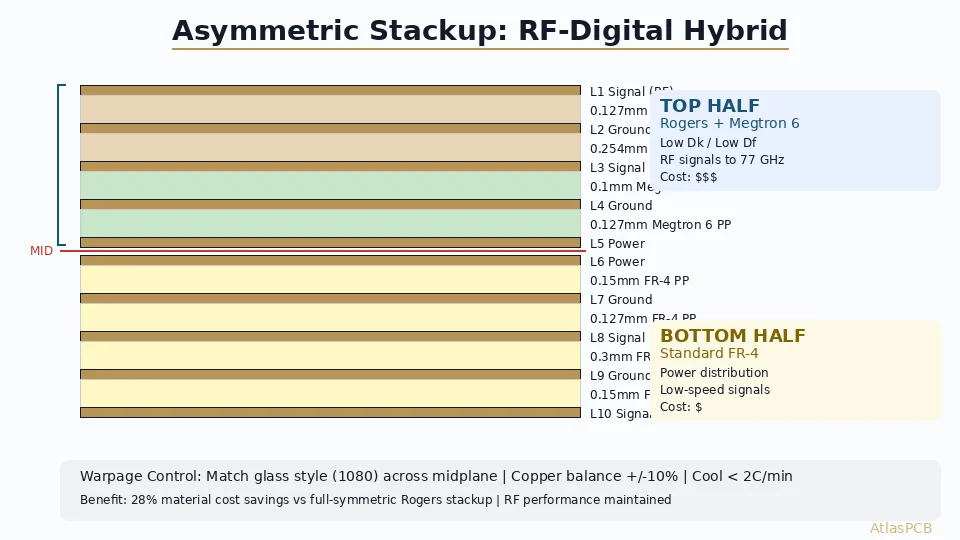
Hybrid Stackups
Mix low-loss material on high-speed signal layers with standard FR4 on other layers. See our [Rogers 4350B vs FR4 comparison]/blog/rogers-4350b-vs-fr4/) for RF hybrid stackup guidance.
Common Stackup Mistakes
Mistake 1: Two Signal Layers With No Reference Between Them
L3 — Signal
    ─── prepreg 4 mil ───
L4 — Signal   ← No reference plane!
This creates broadside coupling between L3 and L4, uncontrolled impedance on both layers, and increased EMI radiation. Always place a ground or power plane between signal layers.
Mistake 2: Referencing a Split Power Plane
A power plane with voltage island splits is not a valid impedance reference across the split boundary. Return current flowing on L3 cannot cross a split on L4 — it must find an alternative path, which increases loop area and EMI.
Solution: Use solid ground planes as primary references. If signal traces must cross a power plane split, provide a ground stitching via near the crossover point.
Mistake 3: Ignoring Prepreg Availability
Specifying 3.2 mil dielectric when the manufacturer only has 2.8 mil or 3.5 mil prepreg forces a substitution that changes impedance. Always check material availability before finalizing your stackup.
Mistake 4: Unbalanced Copper
Layers 1-6 with heavy copper pours and layers 7-12 with sparse routing create an imbalance that warps the board. Check total copper area per layer and add thieving (dummy copper fill) on sparse layers.
Mistake 5: No Margin for Manufacturing Variation
Designing impedance at exactly 50.0Ω with zero margin means any manufacturing variation puts you out of spec. Target the center of your tolerance band and verify that worst-case material variation stays within limits.
Working With Your Manufacturer on Stackup Design
The most efficient stackup design process:
- Start with your requirements — layer count estimate, impedance targets, total thickness constraint, material preference
- Send preliminary stackup to manufacturer — before routing, not after
- Manufacturer simulates impedance — returns trace widths for each target on each layer
- You design with those trace widths — now routing matches manufactured impedance
- Final verification — manufacturer re-simulates after Gerber output to confirm
This process avoids the common problem of finishing routing, sending to a manufacturer, and discovering that your impedance does not work on their available materials — requiring a re-stackup and re-route.
How Atlas PCB Handles Stackup Design
Stackup engineering is included with every controlled impedance order:
- Pre-production stackup simulation using Polar SI with material-specific Dk data
- Trace width calculation for every impedance target on every layer
- Material mapping — your specified dielectrics mapped to available prepreg and core from current stock
- Symmetry verification — copper balance checked for warpage risk
- Total thickness confirmation — verified against your mechanical constraints
- Field solver report provided with impedance predictions per layer
Every order includes a 12-hour engineering pre-audit. Stackup issues are caught and resolved before production — not discovered during debugging.
Frequently Asked Questions
How do I decide how many layers my PCB needs?
Layer count depends on routing density, impedance control requirements, power delivery needs, and physical constraints. A rough guide: 4 layers for designs under 500 nets with controlled impedance, 6-8 layers for 500-2000 nets with multiple power rails, 10-16 layers for high-density designs with BGA components and multiple impedance targets, and 20+ layers for server-class boards, backplanes, or very high pin-count FPGAs. The most reliable method is to attempt routing at a given layer count — if auto-router completion drops below 85%, add 2 layers and try again.
What is the most important rule for multilayer stackup design?
Every high-speed signal layer must have an adjacent reference plane (ground preferred). This single rule ensures controlled impedance, provides a return current path, and minimizes EMI. Breaking this rule by placing two signal layers adjacent to each other creates crosstalk, uncontrolled impedance, and EMI issues that cannot be fixed by routing alone.
Why does stackup symmetry matter?
Asymmetric copper distribution above and below the board center causes warpage during lamination and reflow. The high-copper side contracts less during cooling, bending the board. For IPC Class 2 boards, warpage must stay below 1.5%; for Class 3, below 0.75%. Symmetric stackups — mirroring layer types, copper weights, and dielectric thicknesses around the center — inherently minimize warpage without requiring post-lamination stress relief.
Summary
- Every signal layer needs an adjacent reference plane — this is the non-negotiable rule
- Stackup symmetry prevents warpage — mirror everything around the center axis
- Coordinate dielectric thicknesses with your manufacturer before routing
- Place high-speed signals on inner stripline layers for best impedance control
- Pair power and ground planes with thin dielectric (2-4 mil) for decoupling
- Get impedance simulated on the actual stackup with actual materials before routing
Need help designing your multilayer stackup? Upload your Gerbers for a free engineering review including stackup simulation and impedance verification. Or talk to an engineer about your specific layer count and impedance requirements.
Related guides: [Multilayer FR4 PCB Manufacturer]/blog/multilayer-fr4-pcb-manufacturer/) | [PCB Impedance Control]/blog/pcb-impedance-control/) | [PCB Materials Guide]/blog/pcb-materials-guide/)
Further Reading
[PCB Sequential Lamination: Process, Design Rules, and When You Need It]/blog/pcb-sequential-lamination/)
[Controlled Impedance PCB: Design, Stackup & Testing Explained]/blog/controlled-impedance-pcb/)
[High-Multilayer FR4 vs Standard FR4: When to Upgrade Material Grade]/blog/high-multilayer-fr4-vs-standard-fr4/)
[PCB Manufacturer with Engineering Review: Why Human DFM Audit Matters]/blog/pcb-manufacturer-engineering-review/)
[PCB Solder Mask: Types, Colors, and Functions Explained]/blog/pcb-solder-mask-guide/)
[HDI PCB Design Guide: Stackup Rules, Via Structures & DFM Checklist]/blog/hdi-pcb-design-guide/)
[PCB DFM Checklist: 50 Points to Review Before Sending Gerbers]/blog/pcb-dfm-checklist/)
[RF PCB Materials Comparison: FR4 vs Rogers vs Taconic vs Isola]/blog/rf-pcb-materials-comparison/)
[BGA Escape Routing: Strategies for 0.4mm, 0.5mm, and 0.8mm Pitch]/blog/bga-escape-routing/)
[IPC Class 2 vs Class 3: Which Standard Does Your Board Need?]/blog/ipc-class-2-vs-class-3/)
About AtlasPCB — We specialize in complex PCB manufacturing for HDI, RF, and high-reliability applications. Explore our impedance-controlled PCB manufacturing . Every order includes free engineering review. Get your quote.
Reviewed by AtlasPCB Engineering Team — IPC-certified manufacturing specialists with 15+ years of production experience in HDI, RF, and high-reliability PCB fabrication. Content based on factory floor data and real customer design reviews.
- pcb stackup
- multilayer design
- impedance planning
- layer assignment
- signal integrity