· AtlasPCB Engineering · Engineering · 9 min read
Controlled Impedance PCB: Design, Stackup & Testing Explained
Complete guide to controlled impedance PCB design. Covers impedance targets, stackup planning, trace geometry, dielectric selection, TDR testing, and manufacturing tolerances for single-ended and differential pairs.
Controlled impedance is not optional for modern digital and RF designs. Every high-speed serial interface — USB, PCIe, HDMI, Ethernet, DDR — specifies impedance targets. Every RF trace requires controlled impedance for proper power transfer and minimal reflections.
This guide covers the physics, design rules, manufacturing processes, and testing methods you need to specify controlled impedance correctly.
What Is Controlled Impedance?
Characteristic impedance is a property of a transmission line — it describes the ratio of voltage to current for a wave propagating along the trace. It is determined by the trace geometry and surrounding dielectric material, not by trace length or DC resistance.
A “controlled impedance” PCB means the manufacturer guarantees specific impedance values on designated traces, verified by measurement.
Common Impedance Targets
| Interface | Impedance Target | Type | Tolerance |
|---|---|---|---|
| General single-ended | 50Ω | Single-ended | ±10% |
| USB 2.0 | 90Ω differential | Differential pair | ±15% |
| USB 3.x / USB4 | 85Ω differential | Differential pair | ±10% |
| PCIe Gen1-3 | 85Ω differential | Differential pair | ±10% |
| PCIe Gen4-5 | 85Ω differential | Differential pair | ±5-7% |
| HDMI 1.4/2.0 | 100Ω differential | Differential pair | ±10% |
| DDR3/DDR4 | 40-60Ω single-ended | Single-ended | ±10% |
| DDR5 | 40Ω single-ended | Single-ended | ±5-10% |
| 10G/25G Ethernet | 100Ω differential | Differential pair | ±5-10% |
| 100G Ethernet | 92-100Ω differential | Differential pair | ±5% |
| RF (general) | 50Ω | Single-ended | ±5% |
| LVDS | 100Ω differential | Differential pair | ±10% |
| MIPI CSI/DSI | 100Ω differential | Differential pair | ±10% |
Why Impedance Matters
When a signal encounters an impedance discontinuity (e.g., a 50Ω trace connected to a 75Ω section), part of the signal energy reflects back toward the source. The reflection coefficient is:
Γ = (Z₂ - Z₁) / (Z₂ + Z₁)For a 50Ω trace hitting a 60Ω discontinuity: Γ = 0.091 (9.1% voltage reflection). This reflection degrades signal quality, causes ringing, and at high frequencies creates standing waves that distort the signal envelope.
Bottom line: Uncontrolled impedance = uncontrolled reflections = unpredictable signal integrity.
Physics of PCB Impedance
Transmission Line Structures
Four trace structures are used in PCBs:
Microstrip (outer layer trace over ground plane):
| Parameter | Effect on Impedance |
|---|---|
| Trace width ↑ | Impedance ↓ |
| Dielectric thickness ↑ | Impedance ↑ |
| Dielectric constant (Dk) ↑ | Impedance ↓ |
| Copper thickness ↑ | Impedance ↓ (minor) |
Approximate formula:
Z₀ ≈ (87 / √(Dk + 1.41)) × ln(5.98h / (0.8w + t))where h = dielectric thickness, w = trace width, t = copper thickness
Stripline (inner layer trace between two ground planes):
| Parameter | Effect on Impedance |
|---|---|
| Trace width ↑ | Impedance ↓ |
| Dielectric thickness ↑ | Impedance ↑ |
| Dielectric constant (Dk) ↑ | Impedance ↓ |
| Trace position (asymmetry) | Slight impedance shift |
Stripline impedance is typically 10-15% lower than microstrip for the same trace width and dielectric thickness, because the trace is fully enclosed in dielectric (higher effective Dk).
Edge-coupled differential pair (two parallel traces, same layer):
Differential impedance depends on single-ended impedance plus coupling:
Z_diff ≈ 2 × Z₀ × (1 - k)where k is the coupling coefficient (determined by trace spacing)
Broadside-coupled differential pair (two traces on adjacent layers, overlapping):
- Used when surface area is constrained
- Tighter coupling, lower differential impedance for same trace width
- Requires precise layer-to-layer registration
Key Relationships
| To Increase Impedance | To Decrease Impedance |
|---|---|
| Narrow the trace | Widen the trace |
| Increase dielectric thickness | Decrease dielectric thickness |
| Use lower Dk material | Use higher Dk material |
| Increase differential pair spacing | Decrease differential pair spacing |
| Use thinner copper | Use thicker copper (minor effect) |
Stackup Design for Impedance Control
The Foundation of Impedance Control
Impedance is a stackup-level decision, not a trace-level decision. You cannot achieve controlled impedance without a well-defined, manufactured-to-spec stackup.
4-Layer Stackup Example (Standard)
Layer 1: Signal (microstrip) — 1oz copper
         Prepreg: 1080, 4.2mil, Dk 4.2
Layer 2: Ground plane — 1oz copper
         Core: 39mil, Dk 4.4
Layer 3: Power plane — 1oz copper
         Prepreg: 1080, 4.2mil, Dk 4.2
Layer 4: Signal (microstrip) — 1oz copper
Target impedances:
- 50Ω single-ended microstrip on L1/L4: Trace width ≈ 7.0mil
- 100Ω differential microstrip on L1/L4: Trace width ≈ 5.5mil, space ≈ 5.5mil
6-Layer Stackup Example (High-Speed)
Layer 1: Signal (microstrip) — ½oz copper
         Prepreg: 1080×2, 7.5mil, Dk 4.2
Layer 2: Ground plane — 1oz copper
         Core: 8mil, Dk 4.4
Layer 3: Signal (stripline)
         Prepreg: 1080×2, 7.5mil, Dk 4.2
Layer 4: Power plane — 1oz copper
         Core: 8mil, Dk 4.4
Layer 5: Ground plane — 1oz copper
         Prepreg: 1080×2, 7.5mil, Dk 4.2
Layer 6: Signal (microstrip) — ½oz copper
Target impedances:
- 50Ω microstrip on L1/L6: Trace width ≈ 12.5mil
- 50Ω stripline on L3: Trace width ≈ 8.5mil
- 100Ω diff microstrip on L1/L6: Trace width ≈ 5.0mil, space ≈ 6.0mil
- 100Ω diff stripline on L3: Trace width ≈ 4.5mil, space ≈ 5.0mil
Material Selection Impact
| Material | Dk @ 1GHz | Dk Tolerance | Impedance Predictability |
|---|---|---|---|
| Standard FR4 | 4.2-4.5 | ±0.2-0.3 | Moderate — Dk varies by lot |
| Low-loss FR4 (e.g., Panasonic Megtron 4) | 3.8-4.0 | ±0.1-0.15 | Good |
| High-performance (e.g., Megtron 6) | 3.65-3.75 | ±0.05-0.10 | Very good |
| Rogers 4003C | 3.38 | ±0.05 | Excellent |
| Rogers 4350B | 3.48 | ±0.05 | Excellent |
For ±5% impedance tolerance, specify material with Dk tolerance ≤±0.10. Standard FR4 with ±0.3 Dk variation makes ±5% impedance very difficult — a 5% Dk shift produces approximately 2.5% impedance change, consuming half your budget before manufacturing variation.

Designing for Controlled Impedance
Step 1: Define Your Requirements
Before touching the layout tool, document:
- Which nets require impedance control (identify by interface)
- Target impedance and tolerance for each
- Single-ended vs. differential
- Which layers each interface routes on
- Maximum acceptable insertion loss (determines material grade)
Step 2: Work with Your Manufacturer
Do not calculate impedance in isolation. Your manufacturer knows:
- Actual Dk of the specific material lot they will use
- Their etch factor (trapezoidal trace profile, not rectangular)
- Their pressed dielectric thickness (prepreg thickness changes under pressure)
- Their copper plating thickness on inner/outer layers
Provide your impedance requirements; let the manufacturer’s impedance modeling tool (typically Polar Si9000 or equivalent) determine the trace widths for their specific process.
Step 3: Design Rule Setup
Based on the manufacturer’s impedance model, set up design rules:
| Parameter | Source | Example |
|---|---|---|
| Single-ended trace width | From impedance model | 7.0 ±0.5 mil |
| Differential pair trace width | From impedance model | 5.5 ±0.5 mil |
| Differential pair spacing | From impedance model | 5.5 ±0.5 mil |
| Trace-to-copper clearance | ≥3× dielectric thickness | 12.6 mil |
| Ground void keepout | No ground plane gaps under controlled-impedance traces | — |
| Via keepout | No vias within 20mil of differential pairs | — |
Step 4: Layout Rules
- Maintain consistent trace width on impedance-controlled nets (no tapers except at transitions)
- Reference plane continuity — no splits or gaps in the reference ground/power plane under controlled-impedance traces
- Length matching — differential pairs require matched electrical length (physical length adjusted for any asymmetry)
- Consistent spacing — differential pair spacing must not vary (any change creates a local impedance discontinuity)
Engineer’s Note: The most common impedance failure in layout review is a ground plane slot under a high-speed trace. When the return current path is interrupted, impedance spikes and the signal sees a discontinuity. Always verify reference plane integrity under every controlled-impedance route.
TDR Testing: How Impedance Is Verified
What Is TDR?
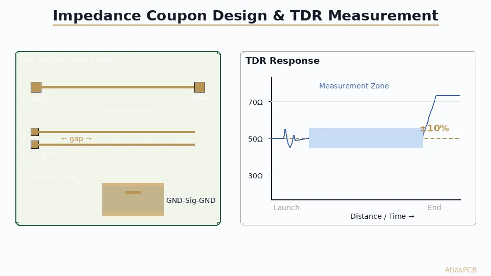
Time Domain Reflectometry (TDR) sends a fast-rise-time step pulse (typically 35ps rise time) into a transmission line and measures the reflected signal. The reflected waveform is mathematically converted to impedance as a function of position along the trace.
TDR Coupon Design
Every controlled-impedance panel includes test coupons — dedicated traces with known geometry matching the production traces:
| Coupon Type | What It Verifies |
|---|---|
| Single-ended microstrip | 50Ω outer layer traces |
| Single-ended stripline | 50Ω inner layer traces |
| Differential microstrip | 100Ω outer layer differential pairs |
| Differential stripline | 100Ω inner layer differential pairs |
| Edge-coupled | Coupling-sensitive traces |
Coupon requirements:
- Length: ≥150mm (6 inches) for adequate measurement window
- SMA or GSSG probe launch pads
- Match exact trace width, spacing, and layer as production traces
- Located at panel edge (waste area)
Reading a TDR Report
A TDR report typically includes:
| Field | Description |
|---|---|
| Coupon ID | Which test structure was measured |
| Target impedance | Design target (e.g., 50Ω) |
| Tolerance | ±5% or ±10% |
| Measured impedance | Average impedance of the coupon trace |
| Min/Max | Minimum and maximum impedance along the trace |
| Pass/Fail | Whether all points fall within tolerance |
| Equipment | TDR model and calibration date |
What to look for: Impedance should be flat across the trace length. Dips or spikes indicate localized geometry changes (etch variation, dielectric thickness change, or measurement artifact).
Manufacturing Factors That Affect Impedance
| Factor | Effect | Manufacturer’s Control |
|---|---|---|
| Etch variation | Trace width ±0.5-1.0mil → impedance ±2-5% | Inner layer: better; outer layer: more variation |
| Dielectric thickness | Prepreg press variation ±0.5-1.0mil → impedance ±3-5% | Material selection, press recipe |
| Dk variation (lot-to-lot) | ±0.1-0.3 depending on material → impedance ±1-3% | Material qualification, incoming inspection |
| Copper weight variation | ±10% standard → impedance ±0.5-1% | Minor factor |
| Copper plating (outer) | 20-35μm addition → impedance shift | Compensate in trace width calculation |
| Etch factor (trapezoidal profile) | Bottom width > top width → effective impedance change | Model using trapezoidal profile, not rectangular |
| Resin content variation | Changes effective Dk → impedance shift | Material specification, incoming QC |
Etch Compensation
Outer layer traces undergo copper plating (adding ~20-25μm copper) before etching. The plating makes the copper thicker, which changes the etch profile:
Design width:    5.0 mil (top)
                  ╱          ╲
Actual profile:  ╱            ╲    ← trapezoidal
                ┗━━━━━━━━━━━━━┛
                  6.2 mil (bottom)
Your manufacturer’s impedance model accounts for this trapezoidal profile. If you calculate impedance assuming rectangular traces, your results will be off by 3-8%.
Design Checklist for Controlled Impedance
- Document all impedance-controlled nets with target values and tolerances
- Specify impedance requirements in fabrication notes (not just in schematic)
- Select material grade appropriate for tolerance (±5% needs Dk ≤±0.10 variation)
- Request impedance model from manufacturer before finalizing trace widths
- Verify reference plane continuity under all controlled-impedance traces
- Include TDR coupon specifications in fab drawing
- Maintain consistent trace width — no unintended tapers or width changes
- Match differential pair lengths and spacing
- Specify etch compensation if providing trace widths (or let manufacturer compensate)
- Request TDR test report with shipment
How Atlas PCB Handles Controlled Impedance
Atlas PCB uses Polar Si9000 field solvers for impedance modeling and Polar CITS880s TDR systems for production verification. We model impedance using actual material Dk from incoming lot testing, not generic datasheet values.
Atlas PCB guarantees ±5% impedance tolerance on all controlled-impedance designs, verified by TDR testing on every production panel, with full impedance test reports included in the shipment documentation. Every order includes a 12-hour human engineering review where we verify stackup feasibility, impedance geometry, reference plane integrity, and coupon placement before production.
For designs requiring ±3% tolerance (specialized RF or 56G+ SerDes), we offer enhanced process control with material pre-qualification and 100% TDR screening.
Summary
- Controlled impedance is required for any signal above ~100MHz or any defined high-speed interface
- Impedance is a stackup-level decision — define stackup before layout
- Work with your manufacturer on trace widths — they know their process parameters
- TDR verification on every panel is the standard for production quality assurance
- ±10% tolerance is standard; ±5% requires tighter material and process control
- Reference plane integrity under controlled-impedance traces is the single most important layout rule
Need impedance-controlled boards done right? Upload your Gerbers for a free engineering review — we will model your impedance, verify your stackup, and guarantee ±5% tolerance with TDR verification.
Related guides: [PCB Impedance Control]/blog/pcb-impedance-control/) | [Microstrip vs Stripline]/blog/microstrip-vs-stripline/) | [PCB Material Selection Guide]/blog/pcb-material-selection-guide/) | [Multilayer PCB Stackup Design Guide]/blog/multilayer-pcb-stackup-design-guide/)
Further Reading
[Differential Pair Routing: Rules, Impedance Control, and Layout Best Practices]/blog/differential-pair-routing-pcb/)
[Impedance Controlled PCB Manufacturer: ±5% Guaranteed with TDR Testing]/blog/impedance-controlled-pcb-manufacturer/)
[High-Speed PCB Design: Signal Integrity Essentials for Modern Electronics]/blog/high-speed-pcb-design/)
[Rogers 4350B vs FR4: When to Upgrade Your PCB Material]/blog/rogers-4350b-vs-fr4/)
[Rogers 4003C Material Properties: Dk, Df, and Design Considerations]/blog/rogers-4003c-properties/)
[HDI PCB Design Guide: Stackup Rules, Via Structures & DFM Checklist]/blog/hdi-pcb-design-guide/)
[PCB Manufacturer with Engineering Review: Why Human DFM Audit Matters]/blog/pcb-manufacturer-engineering-review/)
[RF PCB Materials Comparison: FR4 vs Rogers vs Taconic vs Isola]/blog/rf-pcb-materials-comparison/)
[PCB Grounding Techniques: Star, Split, and Solid Ground Plane Strategies]/blog/pcb-grounding-techniques/)
About AtlasPCB — We specialize in complex PCB manufacturing for HDI, RF, and high-reliability applications. Explore our impedance-controlled PCB manufacturing . Every order includes free engineering review. Get your quote.
Reviewed by AtlasPCB Engineering Team — IPC-certified manufacturing specialists with 15+ years of production experience in HDI, RF, and high-reliability PCB fabrication. Content based on factory floor data and real customer design reviews.
- controlled impedance
- impedance control
- TDR testing
- pcb stackup
- signal integrity
- differential pair