· AtlasPCB Engineering · Engineering · 9 min read
Microstrip vs Stripline: Routing Strategies for Controlled Impedance PCBs
Engineering comparison of microstrip and stripline transmission line structures. Covers impedance behavior, loss characteristics, EMI performance, routing density, and when to use each topology in multilayer PCB design.

Every controlled impedance trace on a PCB is either a microstrip or a stripline. Understanding the fundamental tradeoffs between these two transmission line topologies is essential for any engineer routing signals above a few hundred megahertz.
This guide provides the quantitative comparison you need to make informed routing layer assignments.
Structural Fundamentals
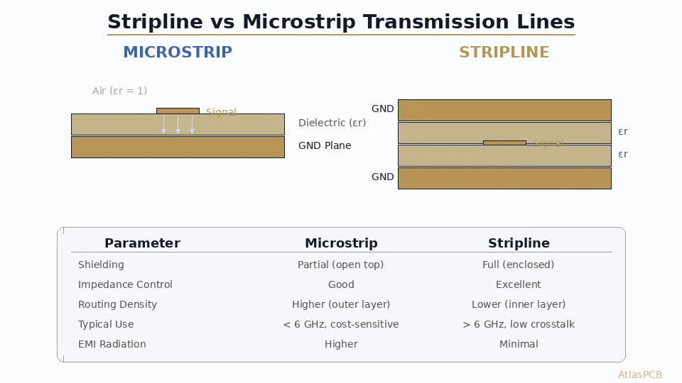
Microstrip
A microstrip transmission line consists of a signal trace on an outer (surface) layer of the PCB, with a continuous reference plane on the adjacent inner layer. The electric field passes partly through the PCB dielectric and partly through air.
          ┌─────────┐
          │  Signal  │  ← Outer copper layer
          └─────────┘
  ═══════════════════════  ← Soldermask (thin)
  ─────────────────────── ← Air (above board)
  ═══════════════════════  ← Board surface
  ╔═══════════════════════╗
  ║    FR4 Dielectric     ║  ← Core/prepreg (h)
  ╚═══════════════════════╝
  ▓▓▓▓▓▓▓▓▓▓▓▓▓▓▓▓▓▓▓▓▓▓▓  ← Reference plane (GND/PWR)
Key parameters: trace width (w), dielectric height (h), copper thickness (t), dielectric constant (Dk).
The effective dielectric constant (Dk_eff) for microstrip is lower than the bulk Dk of the material because part of the field travels through air. For FR4 (Dk ≈ 4.2), Dk_eff for microstrip is typically 3.0-3.5 depending on geometry.
Stripline
A stripline transmission line consists of a signal trace on an inner layer, sandwiched between two continuous reference planes. The electric field is entirely contained within the PCB dielectric.
  ▓▓▓▓▓▓▓▓▓▓▓▓▓▓▓▓▓▓▓▓▓▓▓  ← Reference plane 1 (top)
  ╔═══════════════════════╗
  ║    Dielectric (h1)    ║
  ║    ┌─────────┐        ║
  ║    │  Signal  │        ║  ← Inner copper layer
  ║    └─────────┘        ║
  ║    Dielectric (h2)    ║
  ╚═══════════════════════╝
  ▓▓▓▓▓▓▓▓▓▓▓▓▓▓▓▓▓▓▓▓▓▓▓  ← Reference plane 2 (bottom)
Key parameters: trace width (w), dielectric height above (h1), dielectric height below (h2), copper thickness (t), dielectric constant (Dk).
When h1 = h2, the structure is called symmetric (or balanced) stripline. When h1 ≠ h2, it is asymmetric (or offset) stripline. Most practical stripline implementations are offset because the signal trace sits on a copper layer that is adjacent to a core on one side and prepreg on the other.
Impedance Comparison
50Ω Single-Ended Design Examples
Using standard FR4 (Dk = 4.2, Df = 0.02) with 1oz copper:
| Parameter | Microstrip | Stripline |
|---|---|---|
| Dielectric height (h) | 4.0 mil | 4.5 mil (each side for symmetric) |
| Trace width for 50Ω | 7.0 mil | 4.8 mil |
| Dk effective | 3.25 | 4.2 |
| Propagation velocity | 0.56c | 0.49c |
| Delay per inch | 143 ps | 167 ps |
Stripline requires narrower traces for the same impedance because the field is entirely in dielectric (higher Dk_eff). This can be an advantage (higher routing density) or a disadvantage (tighter manufacturing tolerance required).
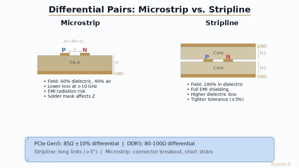
100Ω Differential Pair Examples
| Parameter | Microstrip (edge-coupled) | Stripline (edge-coupled) |
|---|---|---|
| Trace width | 5.0 mil | 3.8 mil |
| Spacing | 5.0 mil | 5.0 mil |
| Differential impedance | 100Ω | 100Ω |
| Common mode impedance | 58Ω | 52Ω |
Manufacturing Tolerance Impact
| Parameter | Microstrip | Stripline |
|---|---|---|
| Typical impedance tolerance | ±7% | ±10% |
| Trace width sensitivity | ~2.5Ω per mil | ~3.5Ω per mil |
| Dielectric height sensitivity | ~4Ω per mil | ~3Ω per mil (each side) |
| Dk variation sensitivity | ~3Ω per 0.1 Dk | ~5Ω per 0.1 Dk |
Microstrip is generally easier to control because it depends on fewer manufacturing variables. The dielectric on one side is air (constant, known), and the dielectric on the other side is a single layer with one Dk value.
Loss Comparison
Loss in PCB transmission lines comes from two sources: conductor loss (copper resistivity) and dielectric loss (dielectric absorption).
Conductor Loss
Conductor loss is proportional to trace resistance per unit length, which depends on copper cross-section and skin depth. At high frequencies, current crowds into a thin skin at the copper surface.
For the same impedance:
- Microstrip traces are wider → lower resistance → lower conductor loss
- Stripline traces are narrower → higher resistance → higher conductor loss
Difference: stripline conductor loss is approximately 15-30% higher than microstrip at the same impedance and frequency.
Dielectric Loss
Dielectric loss is proportional to frequency × Dk_eff × Df.
- Microstrip Dk_eff ≈ 3.0-3.5 (field partly in air)
- Stripline Dk_eff ≈ 4.0-4.2 (field entirely in dielectric)
Stripline has approximately 20-30% higher dielectric loss because the entire field passes through lossy dielectric material.
Total Loss Comparison (FR4, 50Ω)
| Frequency | Microstrip (dB/inch) | Stripline (dB/inch) | Delta |
|---|---|---|---|
| 1 GHz | 0.15 | 0.19 | +27% |
| 5 GHz | 0.45 | 0.56 | +24% |
| 10 GHz | 0.85 | 1.05 | +24% |
| 25 GHz | 1.8 | 2.3 | +28% |
For long traces (>6 inches) at frequencies above 5GHz, the microstrip loss advantage is significant. This is why high-speed serial links (PCIe Gen5/6, 112G PAM4) increasingly favor microstrip or surface-level routing despite the EMI implications.
EMI and Crosstalk
Radiation
This is stripline’s decisive advantage. Because the signal is enclosed between two ground planes, the electromagnetic field is almost entirely contained. Stripline radiates 40-60dB less than microstrip at the same frequency.
For products that must meet FCC Class B, CISPR 32, or MIL-STD-461 emission limits, routing sensitive clocks and high-speed buses on stripline layers can be the difference between passing and failing EMI compliance.
Crosstalk
| Type | Microstrip | Stripline |
|---|---|---|
| Near-end crosstalk (NEXT) | Higher | Lower |
| Far-end crosstalk (FEXT) | Present | Near zero (symmetric) |
| Isolation at 3× trace spacing | ~-25 dB | ~-40 dB |
Stripline’s advantage in crosstalk is particularly dramatic for far-end crosstalk (FEXT). In a symmetric stripline, the electric and magnetic field coupling coefficients are nearly equal, causing forward-traveling crosstalk to cancel. This property does not exist in microstrip.
For high-density routing with many parallel traces (memory buses, LVDS arrays), stripline’s crosstalk advantage directly translates to reduced spacing requirements and higher routing density.
Routing Density and Practical Constraints
Via Transitions
Microstrip signals are on surface layers — accessible for probing and requiring no vias for component connections. Stripline signals require vias for every component connection and every layer transition.
Each via introduces:
- Impedance discontinuity: typically 1-5Ω deviation depending on via geometry and antipad size
- Via stub resonance: an unterminated via stub creates a resonant notch at f = c / (4 × stub_length × √Dk). For a 50mil stub in FR4, the first resonance is at approximately 15GHz
- Insertion loss: ~0.1-0.3 dB per via transition at 10GHz
For signals above 5GHz, via stubs must be managed through back-drilling (controlled-depth drilling to remove the stub) or by using blind/buried vias that terminate at the target layer.
Test Access
Microstrip traces are accessible for probing, measurement, and rework. Stripline traces are buried and can only be accessed through vias brought to the surface. This matters for:
- Development and debug (oscilloscope probing)
- Manufacturing test (bed-of-nails or flying probe)
- Rework and repair
Layer Count Impact
Stripline requires two reference planes per signal layer. A 4-layer board can have at most one stripline routing layer (between two ground planes). Microstrip layers only need one reference plane each.
For layer-count-constrained designs (cost-sensitive products), microstrip maximizes routing capacity per layer.
Design Guidelines by Application
High-Speed Serial Links (PCIe, USB, Ethernet)
Recommendation: Microstrip preferred for short channels (<6 inches); stripline for longer channels or EMI-sensitive enclosures.
Modern SerDes protocols (PCIe Gen4+, USB 3.2+, 25G+ Ethernet) operate at frequencies where channel loss is the primary design constraint. Microstrip’s ~20% loss advantage extends the reach of the channel. However, if the product must meet strict EMI limits (automotive, medical), stripline with back-drilled vias is the safer choice.
DDR Memory Interfaces
Recommendation: Stripline strongly preferred.
DDR buses are wide (32-64 data bits + address/command), parallel, and highly sensitive to crosstalk. Stripline’s superior crosstalk isolation allows tighter trace spacing, which is essential for routing DDR buses within the length-matching constraints. The loss penalty is acceptable because DDR trace lengths are typically short (1-3 inches).
Clock Distribution
Recommendation: Stripline mandatory for high-frequency clocks.
Clock signals are the primary source of EMI in most digital systems. Routing clocks on stripline layers reduces radiated emissions by 40-60 dB compared to microstrip. This single routing decision often determines EMI compliance outcome.
RF and Analog Signals
Recommendation: Microstrip preferred for most RF applications.
RF circuits require accessible test points, tuning capability, and the lowest possible loss. Microstrip provides all three. Edge-coupled microstrip filters, couplers, and matching networks are standard RF design elements that cannot be implemented in stripline.
Exception: RF signals in high-density mixed-signal designs where isolation from digital noise is critical may benefit from stripline routing.
Practical Stackup Strategies
6-Layer General Purpose
L1: Microstrip (components, short high-speed, RF)
L2: Ground plane (reference for L1, shield for L3)
L3: Stripline (high-speed bus, clocks, sensitive signals)
L4: Power plane (reference for L3 and L5)
L5: Stripline (high-speed bus, clocks, sensitive signals)
L6: Microstrip (components, short high-speed, RF)
8-Layer High-Speed
L1: Microstrip (components, SerDes TX/RX)
L2: Ground plane
L3: Stripline (DDR, clocks)
L4: Power plane
L5: Ground plane
L6: Stripline (DDR, clocks)
L7: Ground plane
L8: Microstrip (components, SerDes TX/RX)
At Atlas PCB, we review every stackup during our engineering pre-audit to verify impedance targets, layer assignments, and reference plane integrity.
Frequently Asked Questions
Does soldermask affect microstrip impedance?
Yes. Soldermask has a dielectric constant of approximately 3.3-4.0 and is typically 0.5-1.0 mil thick over copper traces. This additional dielectric layer lowers microstrip impedance by 2-5Ω depending on mask thickness and Dk. Most impedance calculators include a soldermask option — always include it in your calculations for microstrip layers. Alternatively, specify soldermask opening over impedance-critical traces, though this is unusual in production.
Can asymmetric stripline achieve the same performance as symmetric?
Asymmetric (offset) stripline has slightly different characteristics than symmetric stripline. The most important difference is that asymmetric stripline does not fully cancel far-end crosstalk (FEXT) — the cancellation that makes symmetric stripline attractive. However, if the offset is moderate (h1/h2 ratio between 0.5 and 2.0), the FEXT degradation is small. Most real-world stripline is asymmetric because signal layers sit between a core and a prepreg with different thicknesses.
At what frequency does the microstrip vs stripline choice start to matter?
Below approximately 100MHz, the choice is primarily about routing convenience and layer assignment — neither loss nor EMI is significantly different. Between 100MHz and 1GHz, EMI differences become measurable, and stripline should be used for clock signals. Above 1GHz, both loss and EMI differences are significant, and the routing layer decision becomes a genuine engineering tradeoff that requires analysis.
Further Reading
[Controlled Impedance PCB: Design, Stackup & Testing Explained]/blog/controlled-impedance-pcb/)
[Differential Pair Routing: Rules, Impedance Control, and Layout Best Practices]/blog/differential-pair-routing-pcb/)
[RF PCB Design Guidelines: Layout, Grounding & Material Selection]/blog/rf-pcb-design-guidelines/)
[EMC/EMI Design for PCBs: Passing Compliance on the First Try]/blog/emc-emi-pcb-design/)
[PCB Grounding Techniques: Star, Split, and Solid Ground Plane Strategies]/blog/pcb-grounding-techniques/)
[HDI PCB Design Guide: Stackup Rules, Via Structures & DFM Checklist]/blog/hdi-pcb-design-guide/)
[RF PCB Materials Comparison: FR4 vs Rogers vs Taconic vs Isola]/blog/rf-pcb-materials-comparison/)
About AtlasPCB — We specialize in complex PCB manufacturing for HDI, RF, and high-reliability applications. Explore our RF and high-frequency PCB services, or get an impedance-controlled PCB manufacturing . Every order includes free engineering review. Get your quote.
Reviewed by AtlasPCB Engineering Team — IPC-certified manufacturing specialists with 15+ years of production experience in HDI, RF, and high-reliability PCB fabrication. Content based on factory floor data and real customer design reviews.
- microstrip
- stripline
- controlled impedance
- signal integrity
- pcb design
- transmission line