· AtlasPCB Engineering · Engineering · 11 min read
RF PCB Design Guidelines: Layout, Grounding & Material Selection
Practical RF PCB design guidelines for engineers working above 1GHz. Covers transmission line design, grounding strategies, component placement, via fencing, material selection, and common RF layout mistakes.
RF PCB design is where electromagnetic theory meets manufacturing reality. A simulation-perfect layout can fail on the bench because of a ground plane slot, an uncontrolled via transition, or a material property that changed between the datasheet value and the manufactured board.
This guide covers practical RF PCB design guidelines — the rules that prevent the most common failures, organized by the design decisions you make in the order you make them.
Design Decision 1: Material Selection
Material selection is the first RF design decision and the hardest to change later. Your choice determines achievable loss, impedance accuracy, and manufacturing complexity for the rest of the design.
Material Selection by Frequency
| Frequency Range | Recommended Material | Rationale |
|---|---|---|
| <1 GHz | Standard FR4 | Loss is negligible on short traces |
| 1-3 GHz | FR4 or Rogers 4003C | Depends on trace length and loss budget |
| 3-10 GHz | Rogers 4003C or 4350B | Stable Dk, manageable loss |
| 10-30 GHz | Rogers 4350B or 5880 | Low Df critical at these frequencies |
| 30-77 GHz | Rogers 5880 or Taconic TLY-5 | Ultra-low loss required |
For a detailed material comparison, see our [Rogers 4350B vs FR4 guide]/blog/rogers-4350b-vs-fr4/).
The Hybrid Stackup Decision
Most RF boards are hybrid designs — RF signal layers on low-loss laminate, digital/power layers on FR4. This reduces cost 40-60% vs. all-RF construction.
Hybrid design rules:
- Place RF laminate on layers that carry RF signals (typically L1 and/or LN)
- Use FR4 for digital signal layers and power/ground layers
- Specify bondply material at the RF-to-FR4 interface (Rogers 4450F or equivalent)
- Maintain board symmetry — if L1 is Rogers, make LN Rogers too
- Use ground planes as buffer layers at the material interface
Design Decision 2: Transmission Line Geometry
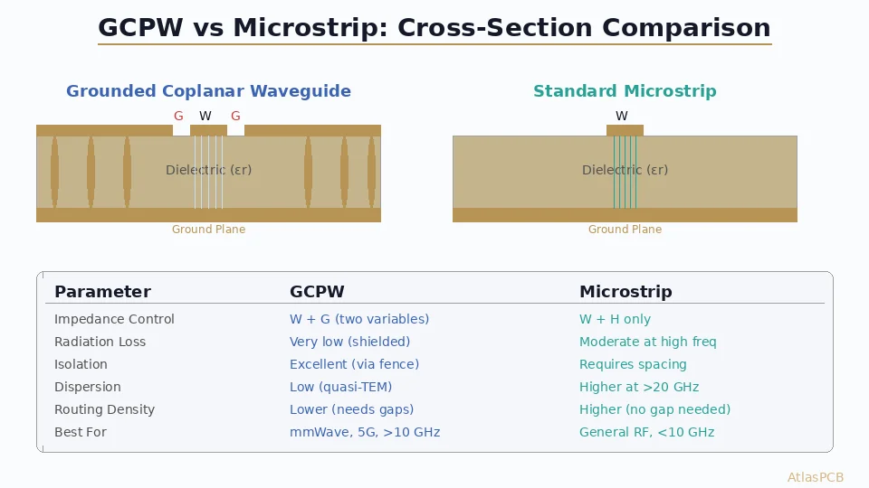
Microstrip vs. Stripline
| Property | Microstrip | Stripline |
|---|---|---|
| Structure | Trace on surface, ground below | Trace between two ground planes |
| Impedance range | 20-120Ω practical | 30-80Ω practical |
| Radiation | Radiates at discontinuities | Shielded — minimal radiation |
| Dispersion | Higher | Lower |
| Effective Dk | ~70-80% of material Dk | ~100% of material Dk |
| Design flexibility | Easy to probe, attach components | Requires via transitions for components |
| Coupling to adjacent traces | Higher | Lower |
When to use microstrip:
- Surface-mount RF components that need direct connection
- Antenna feed lines
- Short RF traces where radiation is acceptable
- Test points and debug access needed
When to use stripline:
- Sensitive traces that need shielding (LNA inputs, oscillator traces)
- Long RF interconnects where radiation must be minimized
- High-isolation requirements between RF channels
- Designs where EMI emissions must be controlled
Impedance Design on RF Materials
For microstrip on Rogers 4003C (Dk 3.38, 20 mil thickness):
| Target Impedance | Trace Width (1oz Cu) | Notes |
|---|---|---|
| 50Ω single-ended | 46 mil (1.17mm) | Standard RF impedance |
| 75Ω single-ended | 25 mil (0.63mm) | Video, some antenna feeds |
| 100Ω differential | 12 mil traces, 8 mil gap | Common for high-speed digital |
Values are approximate — always verify with a field solver using actual material properties.
Critical point: Use Dk at your operating frequency, not the 1MHz datasheet value. Rogers 4003C Dk drops from 3.55 at 1MHz to 3.38 at 10GHz. Using 3.55 for a 10GHz design produces a 2.5% impedance error before any manufacturing tolerance is added.
Design Decision 3: Grounding Strategy
Grounding is the most important aspect of RF PCB layout. More RF problems are caused by poor grounding than by any other design error.
Rule 1: Continuous Ground Plane Under RF Traces
Every RF trace must have a continuous, unbroken ground plane on the immediately adjacent layer. No exceptions.
What “continuous” means:
- No splits or slots crossing under the RF trace path
- No routing of other signals on the ground layer that create gaps
- No power plane cutouts or regions under RF traces
- Via antipads do not create cumulative slots when vias are dense
Why this matters: A slot in the ground plane forces return current to detour around the gap. This detour creates an inductive loop that:
- Changes the trace impedance at the slot location
- Radiates electromagnetic energy (like a slot antenna)
- Couples to circuits on the other side of the ground plane
Even a 0.5mm gap in the ground plane under a 10GHz trace creates a measurable impedance discontinuity.
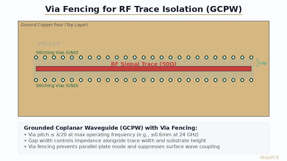
Rule 2: Via Stitching for Ground Continuity
When using multiple ground planes (common in multilayer RF boards), connect them with via stitching:
- Via spacing: ≤λ/20 at the highest operating frequency
- At 10GHz: λ = 30mm, so via spacing ≤1.5mm
- At 5GHz: λ = 60mm, so via spacing ≤3.0mm
- Along RF traces: Via fencing on both sides, spacing ≤λ/10
Via stitching serves two purposes:
- Keeps multiple ground planes at the same potential (prevents parallel plate resonance)
- Creates a via fence that contains electromagnetic fields around RF traces
Rule 3: Component Grounding
RF components (amplifiers, mixers, filters) require low-inductance ground connections. Every ground pad must connect to the ground plane through vias — not through a trace to a distant via.
Best practice: Place multiple vias directly in or immediately adjacent to every RF component ground pad. For QFN ground pads (exposed paddle), use a grid of vias within the paddle area — typically 4-9 vias depending on pad size.
Quantifying “low inductance”: Each via has approximately 0.5-1.0nH of inductance. At 10GHz, 1nH = 63Ω reactance. A single via ground connection to an LNA at 10GHz has 63Ω of ground impedance — unacceptable. Use 4-6 parallel vias to reduce this to 10-15Ω.
Design Decision 4: Isolation and Partitioning
RF-Digital Isolation
Mixed RF+digital boards require physical separation between RF and digital circuits:
- Physical distance — Maintain ≥10mm between RF and digital sections when possible
- Ground plane separation — Use a continuous ground plane but avoid routing digital signals under RF sections
- Power supply isolation — Separate RF and digital power with ferrite beads or LC filters
- Clock routing — Keep digital clocks far from RF sections; clock harmonics fall in RF bands
Channel-to-Channel Isolation
For multi-channel RF systems (e.g., MIMO receivers), isolation between channels is critical:
- Via fences between channels, spacing ≤λ/10
- Separate ground vias for each channel’s return path
- Stripline routing for sensitive channels (provides inherent shielding)
- Physical spacing based on required isolation (>40dB typically needs >5mm + via fence at 5GHz)
Isolation Estimation
| Isolation Method | Typical Isolation @ 5GHz |
|---|---|
| Distance only (10mm) | 20-30 dB |
| Distance + via fence | 40-50 dB |
| Distance + via fence + stripline | 50-60 dB |
| Separate board sections + shield can | 60-80 dB |
Design Decision 5: Via Transitions
Every signal that changes layers passes through a via. At RF frequencies, this via transition is a discontinuity that must be designed, not just placed.
Ground Via Cage
Surround every RF signal via with a ring of ground vias:
- Number of ground vias: 4-8 around each signal via
- Distance from signal via: 2-3x the signal via diameter
- Ground via diameter: Same as signal via or larger
- Purpose: Creates a coaxial-like transition that controls field distribution and minimizes radiation
Via Stub Control
At RF frequencies, the unused portion of a through-hole via (the “stub”) acts as a resonant structure. The quarter-wave resonance frequency of a 1mm stub is approximately 37GHz — but insertion loss degradation begins well below the resonance frequency.
Stub management by frequency:
| Operating Frequency | Maximum Acceptable Stub | Solution |
|---|---|---|
| <3 GHz | 1.5mm | No action needed for most boards |
| 3-10 GHz | 0.5mm | Back-drill or blind vias |
| 10-20 GHz | 0.25mm | Blind vias preferred |
| >20 GHz | <0.1mm | Blind/laser vias mandatory |
For more on via transitions, see our [blind via vs buried via guide]/blog/blind-via-vs-buried-via/).
Design Decision 6: Component Placement
General RF Placement Rules
- Signal flow — Place components in signal-flow order to minimize trace length and crossings
- Short traces — Every millimeter of RF trace adds loss and potential for discontinuities
- Straight traces — Avoid bends when possible; when bending is necessary, use mitered bends (chamfer the outer corner) or curved bends
- Matching components close to the device — Place matching network components as close as possible to the device they serve
- Decoupling at the component — Place RF bypass capacitors within 1mm of the supply pin
Bend Design
When traces must change direction:
- 90° corners: Unacceptable above 1GHz. The excess capacitance at the corner reflects signal.
- 45° mitered bends: Acceptable for most applications. Miter the outer corner at 45°.
- Optimal miter: Remove 60-70% of the corner area (creates a gentle chamfer).
- Curved bends: Best performance. Use a radius ≥3x trace width.
Termination and Matching
Place termination resistors and matching network components on the same layer as the RF trace they connect to. Via transitions to other layers for a matching component defeat the purpose of careful impedance control.
Common RF Layout Mistakes
Mistake 1: Ground Plane Split Under RF Trace
The most common and most damaging RF layout error. Often caused by routing a digital signal on the ground layer that creates a slot under an RF trace.
Impact: Impedance jump + radiation + coupling to signals on the other side of the ground plane.
Fix: Use a different layer for digital routing. Keep the ground layer solid under all RF traces.
Mistake 2: Single Ground Via on RF Component
Connecting an amplifier ground pad to the ground plane with one via. At 10GHz, one via = 63Ω ground impedance.
Impact: Gain reduction, instability, oscillation in amplifiers.
Fix: Multiple ground vias (4-6 minimum) directly under or adjacent to the ground pad.
Mistake 3: Long RF Traces to Save Routing Layers
Running a 10GHz signal 50mm across the board to avoid adding a layer.
Impact: At 10GHz on Rogers 4350B, a 50mm trace loses approximately 0.3dB. On FR4, the same trace loses approximately 1.0dB. If this is your LNA input, you have degraded your system noise figure by 1dB.
Fix: Place the RF signal chain compactly. Add a layer if necessary — it is cheaper than losing 1dB of noise figure.
Mistake 4: No Via Fence Around Sensitive Traces
Running two RF channels 3mm apart on microstrip without via fencing.
Impact: -25dB isolation instead of the -45dB your system requires. Cross-talk between channels.
Fix: Via fence on both sides of each trace, spacing ≤λ/10.
Mistake 5: Ignoring Solder Mask on Impedance
Designing 50Ω microstrip without accounting for solder mask. The mask adds 1-3Ω to microstrip impedance.
Impact: Systematic 2-5% impedance offset on all surface traces.
Fix: Either include solder mask in impedance modeling (recommended) or specify solder mask opening over RF traces (selectively remove mask from RF traces, keeping it elsewhere).
How Atlas PCB Supports RF Design
Atlas PCB provides engineering support specific to RF design challenges:
- Material stocked: Rogers 4003C, 4350B, 5880, Taconic TLY-5 in standard thicknesses
- Hybrid stackup expertise: Proven RF+FR4 hybrid constructions with validated bondply
- Impedance modeling: Field solver using frequency-correct Dk values for the actual material
- Manufacturing capability: PTFE processing (sodium etch, plasma desmear), ±5% impedance with TDR
- Back-drill: Depth-controlled for via stub elimination at high frequencies
Every RF order includes 12-hour human engineering review — covering stackup material compatibility, impedance at operating frequency, via transition analysis, and hybrid interface reliability.
Frequently Asked Questions
What is the most important rule for RF PCB layout?
Maintain an unbroken ground plane directly under every RF trace. Any gap, split, or slot in the ground reference creates impedance discontinuities, radiation, and coupling to other circuits. This single rule prevents more RF failures than all other guidelines combined. If your layout tool shows a ground plane slot under an RF trace, fix it before doing anything else.
When do I need Rogers material instead of FR4 for RF design?
The decision depends on frequency, trace length, and loss budget. Below 1GHz with short traces, FR4 is fine. From 1-3GHz, evaluate your specific insertion loss budget. Above 3GHz, Rogers or equivalent low-loss material is typically required for RF signal traces. For antenna elements, consider Rogers even at lower frequencies because Dk accuracy directly affects radiation pattern and center frequency.
How do I transition from microstrip to stripline in an RF board?
Use a via transition surrounded by a ground via cage. Place 4-8 ground vias in a ring around the signal via, spaced at 2-3x the signal via diameter, with ground via spacing ≤λ/10 at your operating frequency. This creates a coaxial-like structure that minimizes mode conversion and radiation. Keep the signal via stub as short as possible — use back-drilling for frequencies above 5GHz or blind vias for higher frequencies.
Summary
- Continuous ground plane under RF traces is the most important design rule
- Select materials based on operating frequency and loss budget — FR4 below 2GHz, Rogers above 3GHz, evaluate in between
- Use via fences (spacing ≤λ/10) around RF traces and between channels for isolation
- Ground RF components with multiple parallel vias to minimize ground inductance
- Manage via stubs — back-drill or use blind vias above 5GHz
- Mitered or curved bends only — never 90° corners on RF traces
- Include solder mask in microstrip impedance modeling
Designing an RF board? Upload your Gerbers for a free engineering review — we verify impedance, material selection, and hybrid stackup compatibility. Or talk to an engineer to discuss your RF design early in the process.
Related guides: [RF PCB Manufacturer]/blog/rf-pcb-manufacturer/) | [Rogers 4350B vs FR4]/blog/rogers-4350b-vs-fr4/) | [PCB Impedance Control]/blog/pcb-impedance-control/)
Further Reading
- PTFE PCB Manufacturing Services
- Rogers PCB Manufacturing
- Impedance Controlled PCB
- Microstrip vs Stripline: Routing Strategies for Controlled Impedance PCBs
- Rogers 4003C Material Properties: Dk, Df, and Design Considerations
- Taconic TLY-5 PCB: Properties, Applications, and Manufacturing Tips
- PCB Manufacturer with Engineering Review: Why Human DFM Audit Matters
- HDI PCB Design Guide: Stackup Rules, Via Structures & DFM Checklist
- Controlled Impedance PCB: Design, Stackup & Testing Explained
- PCB DFM Checklist: 50 Points to Review Before Sending Gerbers
About AtlasPCB — We specialize in complex PCB manufacturing for HDI, RF, and high-reliability applications. Explore our RF and high-frequency PCB services . Every order includes free engineering review. Get your quote.
Reviewed by AtlasPCB Engineering Team — IPC-certified manufacturing specialists with 15+ years of production experience in HDI, RF, and high-reliability PCB fabrication. Content based on factory floor data and real customer design reviews.
- RF PCB design
- microwave
- transmission line
- grounding
- high frequency layout