· AtlasPCB Engineering · Engineering · 11 min read
PCB Manufacturer with Engineering Review: Why Human DFM Audit Matters
Why automated DRC is not enough for complex PCBs. Learn what a human engineering review catches that software misses, and how to evaluate manufacturers on their pre-production review process.
Every PCB manufacturer advertises “quality” and “engineering support.” Most of them mean automated DRC software that checks your Gerbers against a table of minimum specs and returns a pass/fail report in 5 minutes.
That is not engineering review. That is a file format check.
For complex boards — high layer count, HDI, RF, controlled impedance, tight tolerances — the issues that kill your board are the ones automated tools cannot see. This guide explains what a real engineering review looks like, what it catches, and why it matters.
What Automated DRC Actually Checks
Modern DRC (Design Rule Check) software validates geometric constraints:
- Minimum trace width and spacing
- Minimum drill diameter
- Minimum annular ring
- Pad-to-pad clearance
- Solder mask expansion/opening
- Board outline clearance
- Drill-to-copper clearance
What DRC does well: It catches violations of predefined rules quickly and consistently. Every manufacturer should run DRC on incoming files. It is necessary but not sufficient.
What DRC cannot do:
| What DRC Misses | Why It Matters |
|---|---|
| Stackup feasibility | A 12-layer stackup may pass DRC but be impossible to laminate with available materials |
| Impedance accuracy | DRC does not calculate whether your trace geometry produces 50Ω on the actual stackup |
| Via reliability | A blind via with 1.5:1 aspect ratio passes DRC rules but will fail in production |
| Copper balance | Asymmetric copper distribution causes warpage — invisible to DRC |
| Material compatibility | DRC does not know that standard Tg FR4 is wrong for a 20-layer board |
| Thermal considerations | DRC does not evaluate whether the board survives lead-free reflow |
| Manufacturing-specific limits | Each factory has unique capabilities — DRC uses generic rules |
What Human Engineering Review Catches
A human CAM (Computer-Aided Manufacturing) engineer reviews your files in the context of the specific factory’s capabilities, available materials, and process limits. Here is what that review covers:
1. Stackup Feasibility
Your EDA tool generates a stackup. The manufacturer needs to build it with real materials — and real materials come in specific thicknesses.
Example of what goes wrong: You specify a 10-layer stackup with 4 mil dielectric between layers 3 and 4. The factory’s available prepreg options are 3.5 mil and 4.5 mil. Neither matches your spec. The engineer has to decide: use 3.5 mil (which shifts impedance high) or 4.5 mil (which shifts impedance low). Without human review, the factory picks whichever is in stock.
What the engineer does: Maps your specified dielectric thicknesses to available prepreg and core materials, calculates the impact on impedance, and contacts you if the impedance shift exceeds tolerance. This takes 15-30 minutes for a complex stackup — and saves weeks of debugging impedance failures.
2. Impedance Verification
DRC checks that you have an impedance note in your fab drawing. It does not verify that the specified trace geometry actually produces the target impedance on your stackup.
What the engineer does: Runs your trace width, dielectric thickness (actual, not specified), and copper weight through a field solver. Compares calculated impedance to your target. Identifies any traces that will be out of spec and proposes corrective adjustments (trace width changes or dielectric adjustments).
Common findings:
- Impedance calculated at 52.3Ω when target is 50Ω ±5% — passes, but engineer notes it is near the limit
- Impedance calculated at 54.8Ω when target is 50Ω ±5% — fails. Engineer proposes increasing trace width by 0.3 mil.
- Differential pair impedance is 103Ω when target is 100Ω ±10% — passes, but the spacing-to-width ratio is suboptimal for common-mode rejection
3. Via Structure Analysis
An experienced engineer evaluates via structures for manufacturability and reliability:
Aspect ratio: A 0.25mm via in a 3.0mm board has an aspect ratio of 12:1. Most factories reliably plate up to 10:1. The engineer flags this and proposes either increasing drill size or using blind/buried vias.
Stub length: For high-speed designs, via stubs create resonances. The engineer calculates stub length from the via structure and flags vias that need back-drilling.
HDI stacking: If your design has stacked microvias, the engineer verifies that copper fill is specified and that the stacking order is compatible with the factory’s sequential lamination process.
Buried via span: The engineer verifies that all buried vias fall within valid sub-lamination boundaries — a constraint that your EDA tool may not enforce.
4. Copper Balance Assessment
Unbalanced copper distribution across the board stackup causes warpage during lamination and reflow. This is invisible to DRC but visible to an experienced engineer.
What the engineer checks:
- Total copper area per layer (and per board zone for large boards)
- Symmetry around the board midpoint
- Pour patterns that create uneven copper density
What the engineer recommends: Adding copper thieving in low-density areas, adjusting fill patterns, or adding balance layers. These changes cost nothing in the design but prevent warpage that can make the board un-assemblable.
5. Material Selection Verification
“FR4” appears on thousands of fab drawings without further specification. A human engineer catches:
- Standard Tg FR4 specified for a 16-layer board that needs high-Tg for sequential lamination
- No material specified at all — leaving the factory to choose the cheapest option
- Rogers material specified but no bondply specified for hybrid stackup interface
- Material lead time issues — the specified laminate may require 2-3 weeks to source
6. Manufacturing-Specific Constraints
Every factory has unique capabilities that differ from generic DRC rules:
- Minimum registration tolerance (varies by equipment age and type)
- Minimum plating thickness in high-aspect-ratio vias
- Maximum panel size (your board may not fit their press)
- Back-drill depth accuracy (varies from ±4 mil to ±10 mil between factories)
- Laser drill minimum size (varies between CO2 and UV-YAG equipment)
A human engineer who knows the factory’s specific capabilities catches mismatches that generic DRC rules miss.

Real-World Examples: What Review Caught
Example 1: The Impossible Stackup
The design: 14-layer board, 1.6mm total thickness, controlled impedance on 8 layers.
What DRC said: Pass. All traces meet minimum width, all vias meet minimum drill.
What engineering review found: The specified total thickness of 1.6mm with 14 layers required dielectric thicknesses of 2.5-3.0 mil between most layers. The factory’s thinnest available prepreg was 3.5 mil. The actual minimum achievable thickness was 2.1mm.
Resolution: The engineer contacted the designer with two options: (1) increase board thickness to 2.1mm, or (2) reduce to 12 layers and achieve 1.6mm. The designer chose option 2, which also reduced cost.
Without review: The factory would have built the board at whatever thickness resulted from their standard materials — approximately 2.1mm. The board would not fit the enclosure.
Example 2: The Silent Impedance Failure
The design: 8-layer board with 50Ω single-ended and 100Ω differential impedance.
What DRC said: Pass. Impedance note present in fab drawing.
What engineering review found: The designer specified 6 mil traces on a 4.5 mil dielectric (Dk 4.2) for 50Ω. The field solver calculated 46.3Ω — outside the ±5% tolerance. The designer had used an online calculator with incorrect Dk value for the actual laminate.
Resolution: The engineer adjusted trace width to 5.2 mil to achieve 50.1Ω on the actual stackup and dielectric.
Without review: The board would have been manufactured with 46.3Ω traces. Depending on the application, this might cause signal integrity issues, impedance mismatch at connectors, or fail incoming quality inspection at the assembler.
Example 3: The Warpage Surprise
The design: 6-layer board, 200mm x 150mm, 2oz copper on layers 1-2, 0.5oz on layers 3-6.
What DRC said: Pass.
What engineering review found: Layers 1-2 had 80% copper fill (ground pour + wide traces). Layers 5-6 had 15% copper fill (sparse routing, no pour). The copper imbalance would cause the board to bow toward the heavy copper side — predicted warpage of 1.5%, exceeding the 0.75% IPC Class 3 limit and the 0.5% maximum for BGA assembly.
Resolution: The engineer added copper thieving to layers 5-6 (cross-hatch ground fill in unused areas) and recommended 1oz copper on layers 3-6 instead of 0.5oz to improve balance.
Without review: The board would warp during reflow, causing BGA solder joint opens on one side.
What to Expect from Different Manufacturer Types
| Review Level | What You Get | Typical Turnaround |
|---|---|---|
| No review (cheapest shops) | File format check only, auto-accept | Minutes |
| Automated DRC (commodity) | Geometric rule check, pass/fail report | 30 min - 2 hours |
| Basic human review (mid-tier) | DRC + manual spot check of obvious issues | 4-8 hours |
| Full engineering review (specialist) | Stackup, impedance, via analysis, copper balance, material verification | 8-24 hours |
Price correlation: Full engineering review is typically included in the manufacturer’s pricing for complex boards. It is not a separate line item — it is part of their process. Manufacturers who skip review save cost, which is reflected in lower prices.
The question is not “does review cost extra?” but “does skipping review cost more in failures?”
How to Evaluate a Manufacturer’s Review Process
Ask these questions before placing an order:
“Do you perform human engineering review on every order, or only on request?”
- Good answer: “Every order. Our CAM team reviews files before production.”
- Bad answer: “We can do it if you pay extra for engineering services.”
“How long does your engineering review typically take for a 12-layer controlled-impedance board?”
- Good answer: “4-12 hours depending on complexity.”
- Bad answer: “We review files in real-time” (means automated only).
“What happens if your engineer finds a problem with my design?”
- Good answer: “We contact you with the issue and proposed solution before proceeding.”
- Bad answer: “We adjust as needed to make it manufacturable.” (Silent modification.)
“Can I see a sample DFM report from a previous order?”
- Good answer: Provides a redacted example showing stackup verification, impedance calculation, and DFM comments.
- Bad answer: “We don’t generate reports — we just build the board.”
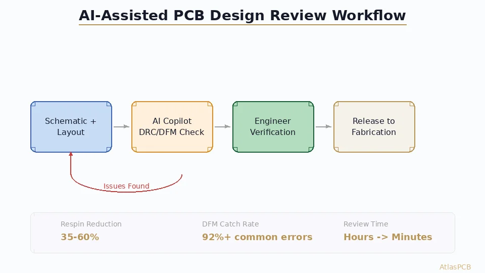
How Atlas PCB’s Engineering Review Works
Every order at Atlas PCB — from 1-piece prototype to production quantity — goes through the same engineering review process:
Within 12 hours of file upload:
- File integrity check — Gerbers complete, drill files present, layer mapping verified
- Stackup verification — Specified stackup mapped to available materials, total thickness confirmed, dielectric thicknesses validated
- Impedance modeling — Every controlled-impedance trace modeled on the actual stackup using a field solver, results compared to targets
- Via analysis — Aspect ratios checked against factory capability, blind/buried via spans validated against sub-lamination plan, stacked vias verified for fill specification
- Copper balance — Per-layer copper distribution assessed, warpage risk evaluated
- Material selection — Laminate grade verified for layer count and thermal requirements
- DFM check — Manufacturing-specific constraints applied (not generic DRC rules)
If issues are found: You receive a detailed report with the issue, impact, and proposed resolution — in English. No changes are made to your design without your approval.
If everything passes: You receive confirmation that your files are production-ready, with the verified stackup and impedance data.
Frequently Asked Questions
What is the difference between DRC and DFM review?
DRC (Design Rule Check) is automated software that checks geometric constraints — minimum trace width, spacing, drill size, annular ring. It is fast and consistent but blind to manufacturing context. DFM (Design for Manufacturability) review is a human engineering assessment that evaluates whether your design will actually work when manufactured at a specific factory — considering material availability, stackup feasibility, impedance accuracy, via reliability, and process-specific limitations. DRC catches rule violations; DFM catches design decisions that will cause failure.
What does a human engineering review catch that automated tools miss?
Human review catches stackup designs that are geometrically valid but cannot be built with available materials, impedance targets that are incompatible with the actual dielectric thickness, via structures that pass DRC but will fail thermal cycling, copper distribution that causes warpage, material grades that are inappropriate for sequential lamination or lead-free reflow, and manufacturing constraints specific to the factory’s equipment. These are contextual issues that require engineering judgment, not just rule checking.
How long should a proper engineering review take?
A thorough review for a complex board (8+ layers, controlled impedance, HDI features) takes 4-12 hours depending on the number of impedance-controlled layers, via complexity, and stackup architecture. Reviews completed in under 1 hour for complex boards are likely automated DRC only. For simple 2-4 layer boards without controlled impedance, 1-2 hours is sufficient. The review investment is small compared to the cost and time of a failed production run.
Summary
- Automated DRC checks geometry; human engineering review checks manufacturability
- The most expensive PCB failures come from issues DRC cannot see: stackup infeasibility, impedance errors, material mismatches, and via reliability risks
- Every complex board (8+ layers, HDI, RF, controlled impedance) should have human engineering review
- Evaluate manufacturers on their review process: who reviews, how long it takes, and what happens when problems are found
- Silent design modifications are the most dangerous failure mode — choose a manufacturer that communicates before changing anything
Want your design reviewed before production begins? Upload your Gerbers for a free 12-hour engineering review — covering stackup, impedance, via structure, and DFM. Or talk to an engineer about your specific design challenges.
Related guides: [PCB DFM Checklist]/blog/pcb-design-rules-trace-width-spacing/) | [PCB Manufacturing Process]/blog/pcb-manufacturing-process/) | [PCB Impedance Control]/blog/pcb-impedance-control/)
Further Reading
[HDI PCB Design Guide: Stackup Rules, Via Structures & DFM Checklist]/blog/hdi-pcb-design-guide/)
[HDI PCB Technology: Microvias, Laser Drilling, and High-Density Design]/blog/hdi-pcb-technology/)
[PCB Sequential Lamination: Process, Design Rules, and When You Need It]/blog/pcb-sequential-lamination/)
[Blind Via vs Buried Via: Design Rules, Cost Impact & When to Use Each]/blog/blind-via-vs-buried-via/)
[Controlled Impedance PCB: Design, Stackup & Testing Explained]/blog/controlled-impedance-pcb/)
[Differential Pair Routing: Rules, Impedance Control, and Layout Best Practices]/blog/differential-pair-routing-pcb/)
[High-Speed PCB Design: Signal Integrity Essentials for Modern Electronics]/blog/high-speed-pcb-design/)
[High-Multilayer FR4 vs Standard FR4: When to Upgrade Material Grade]/blog/high-multilayer-fr4-vs-standard-fr4/)
[PCB DFM Checklist: 50 Points to Review Before Sending Gerbers]/blog/pcb-dfm-checklist/)
[PCB Manufacturing Process: 15 Steps from Gerber to Finished Board]/blog/pcb-manufacturing-process-15-steps/)
About AtlasPCB — We specialize in complex PCB manufacturing for HDI, RF, and high-reliability applications. Explore our free engineering DFM review . Every order includes free engineering review. Get your quote.
Reviewed by AtlasPCB Engineering Team — IPC-certified manufacturing specialists with 15+ years of production experience in HDI, RF, and high-reliability PCB fabrication. Content based on factory floor data and real customer design reviews.
- DFM
- engineering review
- CAM audit
- pcb manufacturer
- design for manufacturing