· AtlasPCB Engineering · Engineering · 8 min read
PCB DFM Checklist: 50 Points to Review Before Sending Gerbers
A comprehensive DFM checklist for PCB designers. 50 verification points covering trace routing, via design, copper balance, stackup, solder mask, silkscreen, and fab notes — organized by category.
Sending Gerbers to a manufacturer without a DFM review is like submitting code without testing. It might work. It probably will not.
This checklist covers 50 verification points organized by category. Work through it after routing is complete and before generating final Gerbers. It will not catch every possible issue — your manufacturer’s engineering review should catch the rest — but it will eliminate the most common and most expensive mistakes.
How to Use This Checklist
- Before layout: Review Sections 1-2 (stackup and technology decisions)
- After routing: Review Sections 3-8 (geometry, via, copper, mask, silkscreen, notes)
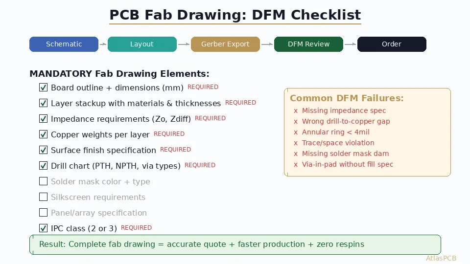
- After Gerber generation: Review Section 9 (output verification)
- Mark N/A for items that do not apply to your design
Section 1: Stackup and Material (6 Points)
- 1.1 Stackup specifies actual material grade (not just “FR4”) — include Tg rating, specific laminate name if critical
- 1.2 Total board thickness is achievable with specified layer count and available prepreg/core thicknesses
- 1.3 Dielectric thicknesses are compatible with target impedance values (verified by field solver, not calculator)
- 1.4 Stackup is symmetric around the midpoint — copper weight, prepreg type, and core thickness are mirrored
- 1.5 High-Tg material specified for boards >8 layers or requiring lead-free reflow at >250°C
- 1.6 RF material specified with exact grade and thickness (Rogers 4003C 20mil, not “Rogers material”)
Section 2: Technology Selection (5 Points)
- 2.1 Minimum trace width is achievable for the specified copper weight (1oz Cu: ≥4mil, 2oz Cu: ≥6mil typical)
- 2.2 Minimum spacing meets manufacturer’s capability for the copper weight
- 2.3 Via types required (through-hole, blind, buried, microvia) are confirmed with manufacturer’s capability
- 2.4 IPC class specified and design rules are compatible (Class 3 requires larger annular ring, see item 4.3)
- 2.5 Surface finish specified (HASL, ENIG, OSP, ENEPIG) and compatible with component requirements (wire bond needs ENEPIG, fine-pitch BGA prefers ENIG)
Section 3: Trace Routing (8 Points)
- 3.1 All traces meet minimum width for the specified copper weight and manufacturer’s capability
- 3.2 All trace spacing meets minimum for voltage rating and manufacturer’s capability
- 3.3 No acid traps — eliminate acute angles (<90°) in copper features where etchant can pool
- 3.4 Differential pairs maintain consistent spacing throughout their length (±10% or tighter)
- 3.5 Differential pair length matching is within specification (typically ±5 mil for high-speed)
- 3.6 No traces routed under board edge that will be cut during depanelization (minimum 0.5mm clearance)
- 3.7 Impedance-controlled traces are on layers specified in the stackup (match fab notes to layout)
- 3.8 No isolated copper features (copper islands) that could float and cause antenna effects or ESD risk
Section 4: Via Design (8 Points)
- 4.1 Through-hole via drill size meets minimum for board thickness (check aspect ratio: thickness ÷ drill ≤ 10:1 standard, ≤8:1 for Class 3)
- 4.2 Via pad size is adequate: pad diameter ≥ drill diameter + 2 × annular ring requirement + 2 × registration tolerance
- 4.3 Annular ring meets IPC class: Class 2 ≥ 0mil (breakout <90°), Class 3 ≥ 1mil (no breakout). Design for ≥5mil to account for registration.
- 4.4 Blind via span is within manufacturer’s capability and sub-lamination plan (verify with manufacturer)
- 4.5 Buried via span is contained within a single sub-lamination core (verify with manufacturer)
- 4.6 Stacked microvias are specified as copper-filled in fab notes (unfilled stacked vias are a reliability failure)
- 4.7 Via-in-pad (if used) is specified as filled and planarized — type specified per IPC-4761 (Type VII for copper fill)
- 4.8 Back-drill vias specify target stub length and reference layer in fab notes (do not assume manufacturer will determine from Gerbers)

Section 5: Copper Balance and Planes (6 Points)
- 5.1 Copper distribution is approximately balanced between top and bottom halves of the stackup (prevents warpage)
- 5.2 Large copper pours have thermal relief connections to pads (prevents tombstoning during reflow)
- 5.3 Ground plane layers are continuous (no large cuts or slots that break return current paths)
- 5.4 Copper thieving or fill added in areas with sparse routing to improve copper balance (reduces warpage and etch uniformity)
- 5.5 No isolated plane islands that could float or cause signal integrity issues
- 5.6 Board edge clearance for copper features ≥ 0.5mm (0.25mm absolute minimum) to prevent copper exposure at board edge
Section 6: Solder Mask (5 Points)
- 6.1 Solder mask expansion (clearance from pad edge to mask edge) is appropriate: 2-3mil for standard, 1.5mil for fine-pitch
- 6.2 Solder mask dams between fine-pitch pads meet manufacturer’s minimum (typically 3-4mil for LPI solder mask)
- 6.3 Via tenting specified where needed (tenting prevents solder from wicking into vias during assembly)
- 6.4 Exposed copper areas (test points, edge connectors, heat sinks) are correctly defined in solder mask layer
- 6.5 Non-functional pads on inner layers — confirm whether solder mask openings are needed (generally not — inner layers do not have solder mask)
Section 7: Silkscreen (4 Points)
- 7.1 No silkscreen over exposed copper pads (silkscreen on pads prevents soldering)
- 7.2 Minimum silkscreen line width meets manufacturer’s capability (typically 4-5mil minimum)
- 7.3 Minimum silkscreen text height is legible (typically 40mil/1mm minimum)
- 7.4 Reference designators placed for post-assembly readability (not hidden under components)
Section 8: Fab Notes and Documentation (5 Points)
- 8.1 Material specification complete: laminate grade, Tg, copper weight per layer, surface finish
- 8.2 Impedance requirements listed with target value, tolerance, trace type (microstrip/stripline), and reference layer
- 8.3 IPC class specified (Class 2 or Class 3) with reference to IPC-6012
- 8.4 Board dimensions and tolerances specified on fab drawing
- 8.5 Special requirements documented: controlled depth drill, back-drill, edge plating, scoring/routing method, panel requirements
Section 9: Output Verification (3 Points)
- 9.1 All Gerber files present and correctly mapped: copper layers, solder mask (top/bottom), silkscreen (top/bottom), paste (top/bottom), board outline, drill files
- 9.2 Drill file includes tool definitions with plated/non-plated designation
- 9.3 Gerbers visually verified in a viewer (Ucamco Reference Gerber Viewer or equivalent) — check for missing features, incorrect mirroring, layer alignment
The Top 10 Most Expensive DFM Mistakes
These are the violations that most often cause board respins, production holds, or field failures:
| Rank | Mistake | Typical Cost |
|---|---|---|
| 1 | Wrong impedance due to incorrect stackup assumption | Full respin + 3-4 weeks |
| 2 | Annular ring violation (Class 3 breakout) | Entire lot rejected |
| 3 | Aspect ratio exceeded — via plating fails | Intermittent field failures |
| 4 | No copper balance — warpage exceeds spec | Lot rejected or assembly failures |
| 5 | Acid traps — etch residue shorts | Random shorts, low yield |
| 6 | Missing impedance spec in fab notes | Manufacturer uses wrong trace width |
| 7 | Stacked microvias without fill spec | Reliability failure in field |
| 8 | Wrong surface finish for application | Solderability or wire bond failure |
| 9 | Missing drill file or wrong format | Production delay, potential re-drill |
| 10 | Board thickness infeasible for layer count | Manufacturer builds at wrong thickness |
How Atlas PCB Uses This Checklist
Every order at Atlas PCB goes through our 12-hour human engineering pre-audit, which covers all 50 points in this checklist plus manufacturing-specific constraints from the factory floor.
What our review adds beyond this checklist:
- Actual material availability mapping (your specified material vs. what is in stock)
- Factory-specific capability limits (not generic industry values)
- Impedance simulation on the actual stackup with actual Dk values
- Historical data from similar builds (known problem areas for comparable designs)
Every order includes this review at no additional cost — from 1-piece prototypes to production runs.
Frequently Asked Questions
What is DFM in PCB design?
DFM (Design for Manufacturability) ensures your PCB design can be reliably manufactured. It covers trace geometry, via design, copper distribution, material selection, and documentation — bridging the gap between what your EDA tool allows and what the factory can actually build. Good DFM practice catches problems that cost thousands of dollars and weeks of time when discovered after fabrication.
When should I run a DFM check on my PCB design?
Run DFM checks at three stages: after schematic review and before layout (stackup and technology decisions), after routing is complete (the most thorough check — all 50 points in this checklist), and after Gerber generation (output file verification). The post-routing check is most critical because it is the last opportunity to catch issues before files go to the factory.
What are the most common DFM violations?
The five most common violations are: insufficient annular ring for registration tolerance (especially on fine-pitch vias), trace width too narrow for the copper weight (1oz Cu needs ≥4mil, 2oz needs ≥6mil), acid traps from acute-angle copper features, missing or incomplete impedance specifications in fab notes, and incomplete drill files (missing tool definitions, no plated/non-plated designation, wrong format).
Summary
- Run this 50-point checklist after routing and before generating Gerbers
- The top cost-saving checks: impedance stackup verification, annular ring for your IPC class, aspect ratio validation, and copper balance
- Fab notes are as important as Gerbers — incomplete notes lead to manufacturer assumptions that may not match your intent
- Your manufacturer should also review your files — this checklist reduces back-and-forth but does not replace engineering review
Ready to get your design reviewed? Upload your Gerbers for a free engineering review — we check all 50 DFM points plus factory-specific constraints. Or [download this checklist as a PDF]/blog/pcb-dfm-checklist/) and use it in your design process.
Related guides: [PCB Manufacturer with Engineering Review]/blog/pcb-manufacturer-engineering-review/) | [PCB Manufacturing Process]/blog/pcb-manufacturing-process/) | [PCB Design Rules]/blog/pcb-design-rules-trace-width-spacing/)
Further Reading
[HDI PCB Technology: Microvias, Laser Drilling, and High-Density Design]/blog/hdi-pcb-technology/)
[Via-in-Pad Design: Filled, Capped, and Plated Over — Complete Guide]/blog/via-in-pad-design/)
[Blind Via vs Buried Via: Design Rules, Cost Impact & When to Use Each]/blog/blind-via-vs-buried-via/)
[Differential Pair Routing: Rules, Impedance Control, and Layout Best Practices]/blog/differential-pair-routing-pcb/)
[Microstrip vs Stripline: Routing Strategies for Controlled Impedance PCBs]/blog/microstrip-vs-stripline/)
[HDI PCB Design Guide: Stackup Rules, Via Structures & DFM Checklist]/blog/hdi-pcb-design-guide/)
[Controlled Impedance PCB: Design, Stackup & Testing Explained]/blog/controlled-impedance-pcb/)
[High-Speed PCB Design: Signal Integrity Essentials for Modern Electronics]/blog/high-speed-pcb-design/)
[Rogers 4003C Material Properties: Dk, Df, and Design Considerations]/blog/rogers-4003c-properties/)
[High-Multilayer FR4 vs Standard FR4: When to Upgrade Material Grade]/blog/high-multilayer-fr4-vs-standard-fr4/)
About AtlasPCB — We specialize in complex PCB manufacturing for HDI, RF, and high-reliability applications. Explore our free engineering DFM review . Every order includes free engineering review. Get your quote.
Reviewed by AtlasPCB Engineering Team — IPC-certified manufacturing specialists with 15+ years of production experience in HDI, RF, and high-reliability PCB fabrication. Content based on factory floor data and real customer design reviews.
- DFM
- design for manufacturing
- pcb checklist
- gerber files
- pcb design review