· AtlasPCB Engineering · Engineering · 9 min read
Via-in-Pad Design: Filled, Capped, and Plated Over — Complete Guide
Comprehensive guide to via-in-pad design for BGA escape routing and high-density PCBs. Covers filled and capped vias, copper plating, IPC standards, solder void prevention, and DFM considerations.
Via-in-pad is not a luxury feature — it is a necessity for modern BGA escape routing. When your package pitch drops below 0.8mm, there is physically no room to route a dog-bone fan-out between pads. The via must go directly in the pad.
But placing a via in a solder pad creates a problem: during reflow, molten solder flows down the via hole (solder wicking), leaving voids in the joint. The solution is filling and capping the via before assembly. This guide covers how to design and specify via-in-pad correctly.
Via-in-Pad Fundamentals
What Is Via-in-Pad?
Via-in-pad (VIP) means placing a plated through-hole or microvia directly within the area of a surface-mount component pad. In standard design practice, vias are placed outside the pad (connected by a short trace or “dog-bone”), but VIP eliminates this offset.
Why Via-in-Pad Exists
Three forces drive via-in-pad adoption:
- BGA pitch reduction — At ≤0.8mm pitch, dog-bone fan-out cannot fit between pads
- Electrical performance — Direct via connection reduces parasitic inductance (critical for decoupling)
- Thermal management — Vias directly under thermal pads provide the shortest thermal path
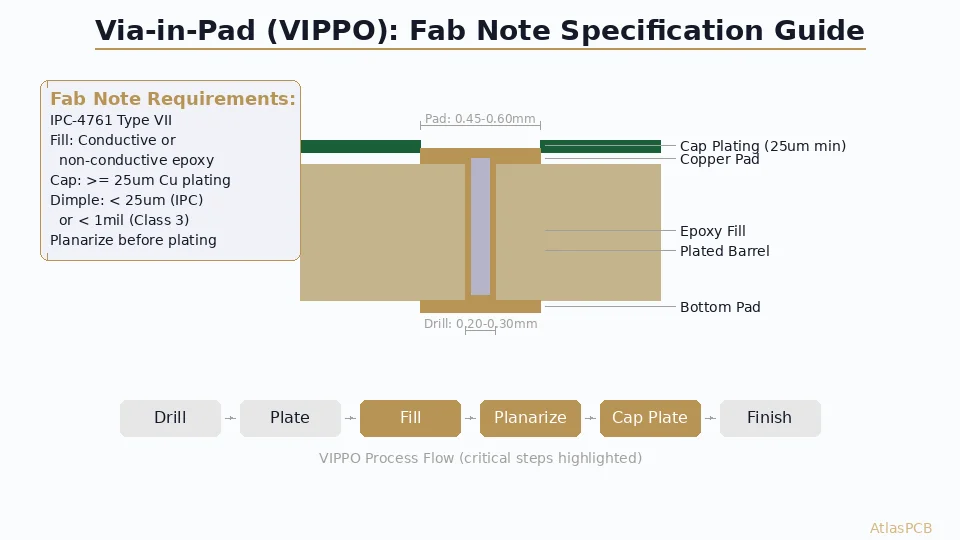
IPC-4761 Via Fill Classifications
IPC-4761 defines seven types of via protection. For via-in-pad, you need to know three:
| IPC-4761 Type | Description | Via-in-Pad Suitable? |
|---|---|---|
| Type I | Tented (dry film covered) | No — film can trap air, void during reflow |
| Type V | Filled (non-conductive) | Marginal — surface may not be flat enough |
| Type VI | Filled (conductive) | Marginal — same surface flatness concern |
| Type VII | Filled and capped (plated over) | Yes — the standard for VIP |
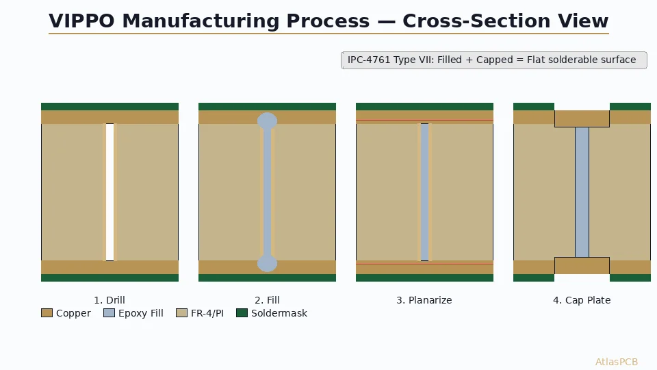
Always specify IPC-4761 Type VII for via-in-pad. This ensures the via is filled with epoxy, planarized (ground flat), then copper-plated to create a surface indistinguishable from a standard pad.
The Via-in-Pad Manufacturing Process
Step-by-Step
- Drill — Mechanical drill (≥8mil) or laser drill (microvia, 3-6mil) creates the via hole
- Electroless + electrolytic copper plate — Standard PTH plating deposits copper on hole walls
- Fill — Non-conductive or conductive epoxy is injected/screened into the via hole
- Cure — Epoxy is thermally cured (typically 150-180°C, 30-60 minutes)
- Planarize — Excess epoxy is ground flat to the copper surface (both sides)
- Cap plate — Additional copper electroplating deposits 15-25μm over the filled via
- Continue processing — Outer layer imaging, etching, solder mask, surface finish
Fill Material Options
| Fill Type | Material | Thermal Conductivity | Typical Use |
|---|---|---|---|
| Non-conductive | Epoxy (e.g., Peters PP2795) | 0.5-1.0 W/m·K | Standard VIP, most applications |
| Conductive (silver) | Silver-filled epoxy | 3-5 W/m·K | Thermal vias, current-carrying vias |
| Conductive (copper) | Copper paste | 8-15 W/m·K | High-current, high-thermal applications |
| Electroplated copper | Solid copper fill | 385 W/m·K | Maximum thermal/electrical performance |
For most BGA escape routing, non-conductive epoxy fill is standard and adequate. Conductive fill is specified when the via must carry significant current or serve as a primary thermal path.
Electroplated Copper Fill
For the highest-performance via fill, some manufacturers offer full electroplated copper fill — the via is plated with copper until completely filled (no epoxy). This provides:
- Highest thermal conductivity (solid copper)
- Highest current capacity
- Best reliability in thermal cycling
- Highest cost (2-3x non-conductive fill)
Electroplated copper fill is common for via diameters ≤10mil (0.25mm). Larger vias are impractical to fill with electroplating due to process time and void risk.
Design Rules
Via Size for Via-in-Pad
The via must be small enough to be reliably filled and large enough to provide adequate plating:
| Via Type | Drill Diameter | Pad Diameter | Fill Method | Max Board Thickness |
|---|---|---|---|---|
| Microvia (laser) | 3-4 mil (75-100μm) | 8-10 mil (200-250μm) | Electroplate copper | 1-2 layers deep |
| Microvia (laser) | 4-6 mil (100-150μm) | 10-14 mil (250-350μm) | Epoxy or electroplate | 1-2 layers deep |
| Small mechanical | 8 mil (200μm) | 16-18 mil (400-450μm) | Epoxy fill | Full board |
| Standard mechanical | 10-12 mil (250-300μm) | 18-22 mil (450-550μm) | Epoxy fill | Full board |
| Large mechanical | 14-16 mil (350-400μm) | 24-28 mil (600-700μm) | Epoxy fill (challenging) | Full board |
Engineer’s Note: Via drill diameter ≤12mil is the practical sweet spot for epoxy-filled VIP. Larger vias (>14mil) are harder to fill without voids, and the fill/planarize cycle becomes less reliable. If your design requires larger vias in pads, consider switching to filled and capped microvias through HDI construction.
BGA Escape Routing with Via-in-Pad
Via-in-pad enables full-field BGA escape. Here is the routing strategy by pitch:
1.0mm pitch BGA:
- Outer 2 rows: Dog-bone fan-out works (0.25mm trace, 0.3mm via between pads)
- Inner rows: Via-in-pad required
- Typical via: 10mil drill, 20mil pad
0.8mm pitch BGA:
- Outer 1 row: Dog-bone fan-out marginally possible
- All inner rows: Via-in-pad required
- Typical via: 8mil drill, 16mil pad
0.65mm pitch BGA:
- All rows: Via-in-pad required (no space for dog-bone)
- Typical via: 4-6mil laser microvia, 10-12mil pad
- HDI construction usually required
0.5mm pitch BGA:
- All rows: Via-in-pad with microvias required
- Typical via: 3-4mil laser microvia, 8-10mil pad
- HDI construction (2-N-2 or higher) required
0.4mm pitch BGA:
- All rows: Via-in-pad with stacked microvias
- Typical via: 3mil laser microvia, 7-8mil pad
- Any-layer HDI construction required
Pad Size Requirements
The pad around a via-in-pad must provide adequate copper for solder joint formation. Minimum pad size is determined by:
- Component pad size (from package datasheet)
- Via drill + annular ring requirement
- Assembly placement accuracy
Rule: The pad must be at least as large as the component pad specified in the datasheet. If the via + annular ring exceeds the component pad, increase the PCB pad accordingly — but check with your assembler that the larger pad does not cause bridging to adjacent pads.
Solder Mask Considerations
Two solder mask approaches for VIP:
Solder Mask Defined (SMD) pad:
- Solder mask overlaps the pad edge
- Pad opening smaller than copper pad
- Better for fine-pitch (≤0.5mm) — masks prevent bridging
- Slightly smaller solder joint
Non-Solder Mask Defined (NSMD) pad:
- Solder mask opening larger than copper pad
- Entire copper pad exposed
- Larger solder joint, better self-alignment during reflow
- Standard for ≥0.65mm pitch
For via-in-pad at ≤0.5mm pitch, SMD pads are generally recommended to prevent solder bridging.
Critical DFM Considerations
Solder Void Prevention
The entire purpose of filling and capping is to prevent solder voids. But even with proper VIP processing, voids can occur if:
| Void Cause | Prevention |
|---|---|
| Incomplete via fill | Specify IPC-4761 Type VII, verify with cross-section |
| Fill material shrinkage | Use low-shrinkage epoxy, verify planarization |
| Cap plating too thin | Specify ≥15μm cap plating thickness |
| Outgassing from fill during reflow | Use fully cured fill material (verify cure cycle) |
| Air trapped under solder paste | Proper stencil design, verify pad flatness |
Acceptance criteria: IPC-A-610 Class 3 allows maximum 25% voiding in BGA solder joints. For via-in-pad joints, Atlas PCB targets <10% voiding through verified fill and cap processes.
Stencil Design for Via-in-Pad
Properly filled and capped VIP pads are flat — standard stencil apertures apply. However, if the cap plating leaves any depression (dimple), adjust:
| Condition | Stencil Aperture Adjustment |
|---|---|
| Flat cap (proper Type VII) | Standard 1:1 aperture |
| Slight dimple (<25μm) | Increase aperture 10-15% to add paste volume |
| Significant dimple (>25μm) | Reject — return to fab for re-planarization |
Aspect Ratio Limits
Via aspect ratio (board thickness : drill diameter) affects plating quality and fill reliability:
| Aspect Ratio | Plating Quality | Fill Reliability | Recommendation |
|---|---|---|---|
| ≤6:1 | Excellent | Excellent | Standard process |
| 6:1 to 8:1 | Good | Good | Specify enhanced plating |
| 8:1 to 10:1 | Marginal | Marginal | Reduce board thickness or increase drill |
| >10:1 | Poor | Poor | Use HDI microvias instead |
For a 1.6mm (62mil) board, maximum reliable VIP drill is 8mil (aspect ratio 7.8:1). For thicker boards, use HDI construction with microvias for via-in-pad connections.
Via-in-Pad for Decoupling Capacitors
Beyond BGA routing, via-in-pad provides a significant electrical benefit for decoupling capacitors.
The Inductance Problem
A standard dog-bone connection from a decoupling capacitor pad to a via adds trace inductance:
| Connection Method | Loop Inductance | Effective Frequency |
|---|---|---|
| Dog-bone, 30mil trace to via | ~1.5 nH | Effective to ~500MHz |
| Dog-bone, 15mil trace to via | ~0.8 nH | Effective to ~1GHz |
| Via-in-pad | ~0.3 nH | Effective to ~3GHz |
At 3GHz+, via-in-pad is the only way to achieve low enough loop inductance for effective decoupling. This is why high-speed FPGA and processor designs universally use VIP for decoupling capacitors.
Layout Pattern
For 0402 or 0201 decoupling capacitors with via-in-pad:
        [Pad 1]          [Pad 2]
         VIP ↓            VIP ↓
    ┌─────────┐      ┌─────────┐
    │  Fill+  │      │  Fill+  │
    │  Cap    │      │  Cap    │
    │  Via    │      │  Via    │
    └────┬────┘      └────┬────┘
         │                │
    Power Plane      Ground Plane
One via connects to the power plane, the other to the ground plane. The inductance is minimized because there is no horizontal trace — just vertical via connections.
HDI Microvia vs Mechanical Via for VIP
| Feature | Laser Microvia VIP | Mechanical Via VIP |
|---|---|---|
| Drill diameter | 3-6 mil (75-150μm) | 8-16 mil (200-400μm) |
| Fill method | Electroplate copper (standard) | Epoxy fill + cap plate |
| Pad size | 8-14 mil (200-350μm) | 16-28 mil (400-700μm) |
| Board thickness coverage | 1-2 layers | Full board |
| Cost | Higher (HDI process) | Lower (standard process) |
| Reliability | Excellent (solid copper fill) | Good (epoxy fill) |
| Thermal performance | Excellent (copper fill) | Moderate (epoxy fill) |
For BGA pitch ≤0.65mm, laser microvia VIP is the only practical option — mechanical drill cannot achieve the required via and pad sizes. See our [HDI PCB Design Guide]/blog/hdi-pcb-design-guide/) for detailed microvia design rules.
Design Checklist for Via-in-Pad
- Confirm VIP is necessary (pitch ≤0.8mm or electrical performance requirement)
- Specify IPC-4761 Type VII (filled and capped) in fab notes
- Select fill material (non-conductive epoxy for standard, conductive for thermal)
- Verify via drill diameter vs. pad size (annular ring ≥4mil)
- Check aspect ratio ≤8:1 for mechanical vias in pad
- Specify cap plating thickness ≥15μm
- Verify pad size meets component datasheet minimum
- Choose SMD vs NSMD pad definition (SMD for ≤0.5mm pitch)
- Add cross-section coupon to panel for fill verification
- Communicate VIP requirement to assembler (stencil design impact)
How Atlas PCB Handles Via-in-Pad
Atlas PCB processes via-in-pad on every HDI and fine-pitch BGA board we manufacture. Our standard VIP process uses non-conductive epoxy fill with copper cap plating ≥20μm, verified by cross-section inspection on every lot.
Atlas PCB supports via-in-pad from 3mil laser microvias to 16mil mechanical vias, with IPC-4761 Type VII fill and cap, cross-section verified fill quality, and ≤10% void acceptance criteria on BGA joints. Every order includes a 12-hour human engineering review where we verify via-in-pad feasibility, pad sizing, and aspect ratios before production — catching issues that automated DRC may not flag.
For BGA escape routing at ≤0.5mm pitch, we routinely build 2-N-2 and 3-N-3 HDI stackups with stacked copper-filled microvias in pad.
Summary
- Via-in-pad is required for BGA escape routing at ≤0.8mm pitch
- Always specify IPC-4761 Type VII — filled and capped with copper plating
- Microvia VIP (laser drill, copper-filled) is standard for ≤0.65mm pitch
- Mechanical VIP (epoxy-filled) works for ≥0.8mm pitch on standard thickness boards
- Aspect ratio ≤8:1 for reliable epoxy fill in mechanical vias
- Decoupling capacitor VIP reduces loop inductance 3-5x vs dog-bone fan-out
Designing a board with fine-pitch BGAs? Upload your Gerbers for a free engineering review — we will verify your via-in-pad specifications and BGA escape routing before production.
Related guides: [HDI PCB Design Guide]/blog/hdi-pcb-design-guide/) | [Blind Via vs Buried Via]/blog/blind-via-vs-buried-via/) | [BGA Escape Routing]/blog/bga-escape-routing/) | [PCB DFM Checklist]/blog/pcb-dfm-checklist/)
Further Reading
[HDI PCB Technology: Microvias, Laser Drilling, and High-Density Design]/blog/hdi-pcb-technology/)
[PCB Manufacturer with Engineering Review: Why Human DFM Audit Matters]/blog/pcb-manufacturer-engineering-review/)
[PCB Manufacturing Process: 15 Steps from Gerber to Finished Board]/blog/pcb-manufacturing-process-15-steps/)
[PCB Surface Finish Guide: HASL, ENIG, OSP and More Compared]/blog/pcb-surface-finish-guide/)
[PCB Solder Mask: Types, Colors, and Functions Explained]/blog/pcb-solder-mask-guide/)
[ENEPIG vs ENIG: Which PCB Surface Finish for Your Design?]/blog/enepig-vs-enig/)
[BGA Soldering and Rework: Challenges, Inspection, and Best Practices]/blog/bga-soldering-rework/)
[PCB Pad Design for BGA, QFN, and Passive Components: Best Practices]/blog/pcb-pad-design-bga-qfn/)
[PCB Thermal Management: Heat Dissipation Techniques for Reliable Electronics]/blog/pcb-thermal-management/)
[PCB Grounding Techniques: Star, Split, and Solid Ground Plane Strategies]/blog/pcb-grounding-techniques/)
About AtlasPCB — We specialize in complex PCB manufacturing for HDI, RF, and high-reliability applications. Explore our HDI PCB manufacturing capabilities . Every order includes free engineering review. Get your quote.
Reviewed by AtlasPCB Engineering Team — IPC-certified manufacturing specialists with 15+ years of production experience in HDI, RF, and high-reliability PCB fabrication. Content based on factory floor data and real customer design reviews.
- via in pad
- BGA routing
- HDI
- pcb design
- filled via
- plated over via