· AtlasPCB Engineering · Engineering · 5 min read
BGA Soldering and Rework: Challenges, Inspection, and Best Practices
Master BGA technology — understand Ball Grid Array soldering challenges, X-ray inspection techniques, common defects (voiding, head-in-pillow, bridging), and professional rework procedures.

Ball Grid Array (BGA) packages offer the highest I/O density and best electrical performance among IC packages. However, their hidden solder joints make them one of the most challenging components to solder, inspect, and rework. This guide covers everything you need to know about BGA assembly.
Why BGA?
Advantages Over QFP/SOIC
- Higher I/O count: 100-2,000+ balls vs 44-256 leads for QFP
- Smaller footprint: Balls under the package, not around the perimeter
- Better electrical performance: Shorter interconnects reduce inductance and improve signal integrity
- Better thermal performance: Large die-attach pad and many thermal balls
- Self-centering: During reflow, surface tension naturally aligns the BGA to its pads
Common BGA Pitches
| Pitch | Ball Count (typical) | Application |
|---|---|---|
| 1.27mm | 100-400 | Legacy, easy to route |
| 1.0mm | 200-700 | Standard digital ICs |
| 0.8mm | 300-1,000 | Processors, FPGAs |
| 0.65mm | 400-1,500 | Advanced processors |
| 0.5mm | 500-2,000 | Mobile SoCs |
| 0.4mm | 500-2,500+ | High-end mobile, AI chips |
BGA Soldering Process
Solder Paste Requirements
- Type 3 paste (25-45um particles) for >=0.65mm pitch
- Type 4 paste (20-38um particles) for 0.5mm pitch
- Type 5 paste (15-25um particles) for 0.4mm and below
- Stencil thickness: 0.10-0.12mm for fine-pitch BGA
Reflow Profile Considerations
- BGA packages have high thermal mass — ensure adequate soak time for temperature equalization
- Maximum delta T across BGA: <10°C during reflow
- Peak temperature: follow IC manufacturer’s MSL (Moisture Sensitivity Level) recommendations
- Cooling rate: 2-4°C/s for optimal solder joint microstructure
PCB Design for BGA
- Pad type: NSMD (Non-Solder Mask Defined) preferred for 0.8mm+ pitch; SMD for <=0.65mm
- Via-in-pad: Required for inner ball rows at <=0.65mm pitch. Must be filled and cap-plated.
- Dogbone routing: For 0.8mm+ pitch, route a short trace to an adjacent via (avoid via-in-pad cost)
- Ground/power planes: Complete planes under BGA for thermal distribution and signal return
BGA Inspection
X-Ray Inspection (Primary Method)
Since BGA solder joints are hidden under the package, X-ray is the only non-destructive way to inspect them.
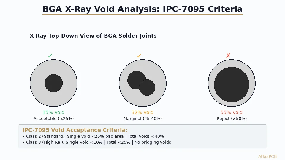
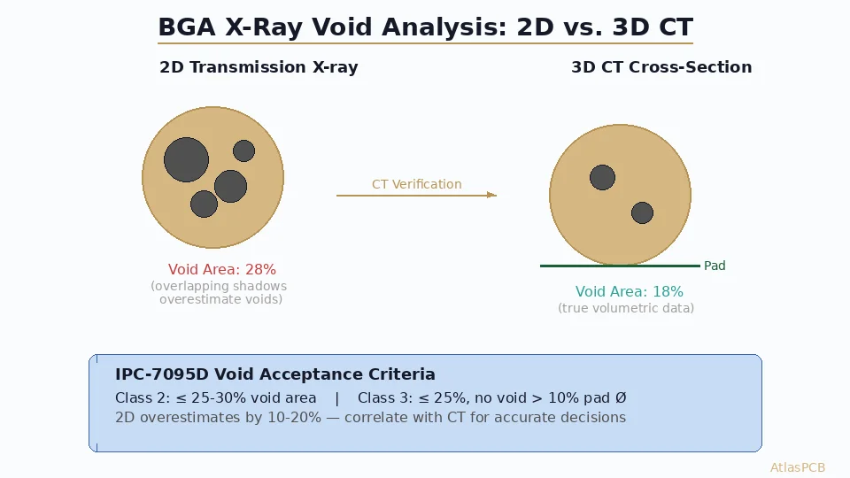
2D X-Ray: Shows a shadow image from one angle. Detects: bridging, missing balls, voiding, misalignment. Fast but limited depth information.
3D CT (Computed Tomography): Reconstructs 3D cross-sections. Can isolate individual ball layers. Detects: head-in-pillow, pad cratering, micro-cracks. Slower but definitive.
What to Look For in X-Ray Images
- Ball shape: Uniform spherical or slightly flattened. Irregular shapes indicate problems.
- Ball alignment: All balls should be on their pads. Offset indicates placement error.
- Bridging: Adjacent balls connected by solder. Caused by excess paste or BGA ball diameter variation.
- Voiding: Dark circles within balls. IPC-7095 allows up to 25% void area per ball.
- Missing balls: Empty pad locations. Either ball was missing from BGA or didn’t wet.

Common BGA Defects
1. Head-in-Pillow (HiP)
The BGA ball touches the paste but doesn’t fully collapse and merge. Creates a partial, unreliable connection.
Cause: Board warpage separates ball from paste during peak reflow temperature.
Prevention: Control warpage (<0.5%), use support pins in reflow oven, optimize reflow profile.
2. Solder Ball Voiding
Trapped flux volatiles create gas bubbles inside solder balls.
Cause: Insufficient preheat, aggressive flux, via-in-pad without fill.
Prevention: Optimize reflow preheat, fill via-in-pad, reduce paste volume for large thermal pads.
3. BGA Bridging
Adjacent solder balls merge together.
Cause: Excessive paste, BGA misalignment, wrong ball size.
Prevention: Verify stencil aperture design, check BGA component quality, verify placement accuracy.
4. Non-Wetting / Cold Joint
Solder doesn’t properly wet the pad or ball surface.
Cause: Oxidized pads or balls, insufficient temperature, expired paste.
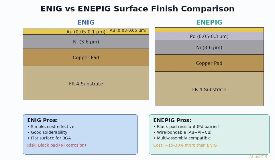
Prevention: Use ENIG finish for BGA sites, verify reflow profile, use fresh paste.
5. Pad Cratering
Fracture in the PCB laminate under the BGA pad, caused by mechanical stress.
Cause: BGA rework at too high temperature, mechanical shock, lead-free solder brittleness.
Prevention: Follow proper rework procedures, use appropriate preheating, handle boards carefully.
BGA Rework
When Rework Is Needed
- Failed BGA must be replaced
- Wrong component placed
- BGA has bridged or open solder joints
- Firmware in BGA package is incorrect (some microcontrollers)
Professional BGA Rework Process
Step 1: Preparation
- Bake the board (125°C, 4 hours) to remove moisture
- Apply liquid flux to the BGA area
- Set up the rework station with correct nozzle size
Step 2: Component Removal
- Preheat board bottom to 150-180°C
- Apply top heat with hot air nozzle (matching BGA outline)
- Ramp to reflow temperature (240-260°C peak)
- When solder melts, lift BGA with vacuum pickup
- Clean pads with solder wick and flux
Step 3: Site Preparation
- Inspect all pads under magnification
- Clean residual solder and flux
- Check for lifted pads or pad cratering
- Apply fresh flux to all pads
Step 4: New Component Placement
- Apply flux to BGA balls or PCB pads
- Place new BGA using vision alignment system
- Verify alignment before reflow
Step 5: Reflow
- Apply the same reflow profile as original assembly
- Monitor with thermocouple if possible
- Allow controlled cooling
Step 6: Post-Rework Inspection
- X-ray to verify all solder joints
- Functional test to verify component operation
- Document rework (for traceability)
Rework Equipment
- BGA rework station: IR or hot-air rework system with bottom preheater. Cost: $5,000-50,000
- Correct nozzle: Must match BGA package size (+/-0.5mm)
- Vision alignment system: Split-prism or camera system for precise alignment
Conclusion
BGA technology enables the high-performance, high-density designs demanded by modern electronics. Success with BGA requires investment in proper PCB design (NSMD pads, via-in-pad, adequate planes), process control (SPI, optimized reflow, SPC), and inspection capability (X-ray). Professional rework capability is essential for prototype and repair scenarios. Work with experienced assembly partners who have proven BGA process capability, especially for fine-pitch (<0.65mm) packages.
Further Reading
[Via-in-Pad Design: Filled, Capped, and Plated Over — Complete Guide]/blog/via-in-pad-design/)
[High-Speed PCB Design: Signal Integrity Essentials for Modern Electronics]/blog/high-speed-pcb-design/)
[ENEPIG vs ENIG: Which PCB Surface Finish for Your Design?]/blog/enepig-vs-enig/)
[PCB Solder Mask: Types, Colors, and Functions Explained]/blog/pcb-solder-mask-guide/)
[PCB Pad Design for BGA, QFN, and Passive Components: Best Practices]/blog/pcb-pad-design-bga-qfn/)
[HDI PCB Design Guide: Stackup Rules, Via Structures & DFM Checklist]/blog/hdi-pcb-design-guide/)
[PCB Surface Finish Guide: HASL, ENIG, OSP and More Compared]/blog/pcb-surface-finish-guide/)
About AtlasPCB — We specialize in complex PCB manufacturing for HDI, RF, and high-reliability applications. Explore our HDI PCB manufacturing capabilities, or get an PCB assembly services . Every order includes free engineering review. Get your quote.
Reviewed by AtlasPCB Engineering Team — IPC-certified manufacturing specialists with 15+ years of production experience in HDI, RF, and high-reliability PCB fabrication. Content based on factory floor data and real customer design reviews.
- BGA
- soldering
- rework
- X-ray inspection