· AtlasPCB Engineering · Engineering · 5 min read
PCB Solder Mask: Types, Colors, and Functions Explained
Everything about PCB solder mask — LPI vs dry film types, color options (green, black, white, red, blue), dam design rules, solder mask opening strategies, and effects on assembly.

The solder mask is the colored coating that gives a PCB its distinctive appearance. But it’s far more than cosmetic — it’s a critical functional layer that affects assembly quality, reliability, and even signal performance. This guide covers everything you need to know.
What Does Solder Mask Do?
- Prevents solder bridging: During reflow or wave soldering, solder mask between pads prevents molten solder from flowing where it shouldn’t
- Protects copper: Prevents oxidation, corrosion, and environmental damage to copper traces
- Electrical insulation: Provides additional insulation between closely spaced traces
- Contamination barrier: Protects against dust, moisture, and handling damage
- Visual contrast: Makes silkscreen text and component outlines easier to read
Solder Mask Types
LPI (Liquid Photo-Imageable) — Industry Standard
The dominant solder mask technology for production PCBs.
Process:
- Liquid epoxy ink is applied via screen printing or curtain/spray coating
- Pre-baked at 75°C to partially cure
- Exposed to UV light through a photomask (or direct imaging)
- Developed to remove unexposed areas (revealing pads)
- Final cure at 150°C
Advantages: High resolution (minimum dam width 3-4 mil), good adhesion, consistent thickness, cost-effective for mass production.
Dry Film Solder Mask
A pre-formed film laminated onto the board surface.
Advantages: Very uniform thickness, good for thick copper boards. Disadvantages: Lower resolution than LPI, higher cost, not suitable for fine-pitch.
Inkjet Solder Mask
Direct digital printing without photomasks.
Advantages: No tooling cost, good for prototypes, can print different colors on the same board. Disadvantages: Lower throughput, higher per-unit cost.
Solder Mask Colors
Green — The Standard
- Why green? Historical reasons: green photoresist was the first to achieve the resolution needed for PCBs, and it provides the best contrast for visual inspection.
- Best inspection contrast: Human eyes are most sensitive to green; defects are easiest to spot.
- Lowest cost: Default color at all manufacturers.
- Best resolution: Green LPI ink achieves the finest feature definition.
Black
- Aesthetics: Premium look for consumer products
- Heat absorption: Absorbs more heat — consider thermal impact
- Inspection difficulty: Harder to visually inspect traces underneath
- Higher cost: Slight premium over green
White
- LED applications: Maximizes light reflection from LED PCBs
- Clean aesthetic: Medical devices, consumer products
- Discoloration risk: Can yellow over time with heat exposure
- Inspection difficulty: Low contrast with silkscreen
Red
- Distinctive appearance: Often used for open-source hardware
- Good contrast: Better than black for visual inspection
- Moderate cost: Slight premium over green
Blue
- Arduino standard: Recognizable for development boards
- Good contrast: Visible traces beneath
- Moderate cost: Similar to red
Matte Black
- Ultra-premium look: Used in high-end consumer electronics
- Anti-glare: Reduces surface reflections
- Highest cost: Among all color options

Solder Mask Design Rules
Solder Mask Opening (SMO) Types
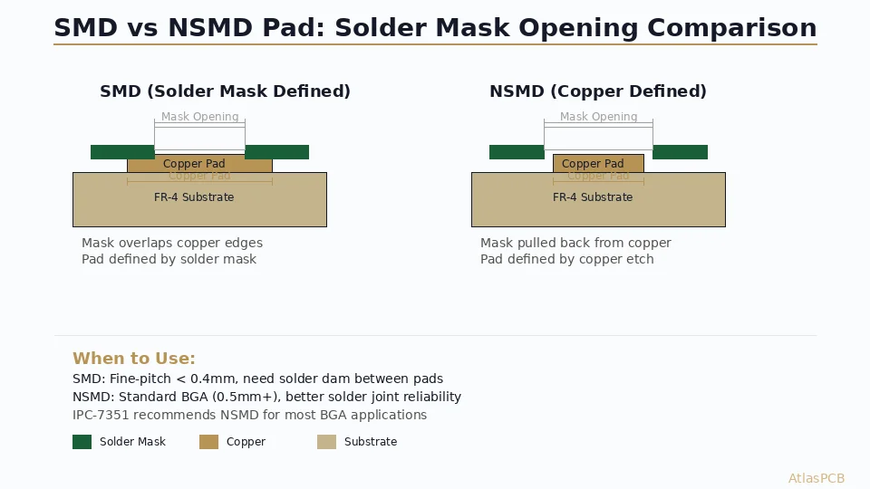
NSMD (Non-Solder Mask Defined):
- Solder mask opening is LARGER than the copper pad
- Copper pad edges are exposed
- Preferred for SMT: Provides larger solderable area and better solder joint reliability
- Typical expansion: 2-3 mil (0.05-0.075mm) per side beyond the copper pad
SMD (Solder Mask Defined):
- Solder mask opening is SMALLER than the copper pad
- Solder mask overlaps the copper pad edges
- Used when: Pad-to-pad spacing is too tight for NSMD, or BGA pad pitch is very fine (< 0.5mm)
- Typical restriction: 2-3 mil per side smaller than the copper pad
Solder Mask Dam
The strip of solder mask between two adjacent pad openings.
| Minimum Dam Width | Capability Level |
|---|---|
| 3 mil (0.075mm) | Advanced |
| 4 mil (0.1mm) | Standard |
| 5 mil (0.13mm) | Conservative |
| 8 mil (0.2mm) | Basic |
If the dam is too narrow: It may wash away during development, leaving no solder mask between pads and increasing the risk of solder bridges.
Solder Mask Clearance on Vias
- Tented vias: Solder mask covers the via completely — prevents solder from wicking into the via during reflow. Recommended for vias near SMD pads.
- Open vias: Via pad is exposed through the solder mask — allows probing but risks solder wicking.
- Plugged and tented: Via is filled with epoxy and covered by solder mask — fully sealed.
Impact on Assembly
Solder Paste Printing
- Solder mask thickness affects stencil-to-board gasketing
- Typical solder mask thickness: 15-25um over copper, 25-40um over substrate
- Inconsistent thickness can cause poor stencil contact and solder paste smearing
Reflow Soldering
- Solder mask acts as a solder dam, containing paste to pad areas
- Green solder mask has the best solder release properties
- Dark colors (black, matte) absorb more IR energy — may need adjusted reflow profiles
Wave Soldering
- Solder mask protects bottom-side SMD components from solder wave
- Minimum solder mask thickness for wave soldering: 20um
Solder Mask and Signal Integrity
At high frequencies (>1 GHz), solder mask affects impedance:
- Solder mask Dk ≈ 3.5-4.0
- Adds parasitic capacitance to outer-layer traces
- For controlled impedance, the field solver must account for solder mask
- Selective solder mask removal over high-speed traces is sometimes used (but adds cost)
Conclusion
Solder mask is a deceptively important PCB layer. Green remains the best default choice for cost, resolution, and inspectability. Choose alternative colors only when aesthetics or specific functional requirements (LED reflection, thermal concerns) demand it. Always specify NSMD openings unless pad spacing forces SMD-defined pads, and work with your manufacturer on minimum dam width capabilities.
Further Reading
[Controlled Impedance PCB: Design, Stackup & Testing Explained]/blog/controlled-impedance-pcb/)
[High-Speed PCB Design: Signal Integrity Essentials for Modern Electronics]/blog/high-speed-pcb-design/)
[PCB Pad Design for BGA, QFN, and Passive Components: Best Practices]/blog/pcb-pad-design-bga-qfn/)
[HDI PCB Design Guide: Stackup Rules, Via Structures & DFM Checklist]/blog/hdi-pcb-design-guide/)
[PCB Manufacturer with Engineering Review: Why Human DFM Audit Matters]/blog/pcb-manufacturer-engineering-review/)
About AtlasPCB — We specialize in complex PCB manufacturing for HDI, RF, and high-reliability applications. Explore our full PCB manufacturing capabilities . Every order includes free engineering review. Get your quote.
Reviewed by AtlasPCB Engineering Team — IPC-certified manufacturing specialists with 15+ years of production experience in HDI, RF, and high-reliability PCB fabrication. Content based on factory floor data and real customer design reviews.
- solder mask
- pcb fabrication
- LPI
- pcb colors