· AtlasPCB Engineering · Engineering · 5 min read
High-Speed PCB Design: Signal Integrity Essentials for Modern Electronics
Master high-speed PCB design — transmission line theory, return paths, crosstalk, power delivery network, and practical guidelines for DDR, PCIe, USB, and Ethernet routing.

When signal edge rates drop below a few nanoseconds, a PCB trace is no longer just a wire — it becomes a transmission line. High-speed PCB design requires understanding signal integrity principles to ensure reliable data transmission. This guide covers the essential concepts and practical guidelines.
When Does “High-Speed” Matter?
Critical length rule: A trace becomes a transmission line when its length exceeds 1/6 of the signal’s electrical wavelength.
For a signal with rise time Tr: Critical length = Tr x v / 6
Where v = propagation velocity (~15cm/ns for FR-4 microstrip)
| Rise Time | Critical Length | Example Interfaces |
|---|---|---|
| 10ns | 25cm | SPI <10MHz, I2C |
| 2ns | 5cm | USB 2.0, 100M Ethernet |
| 500ps | 1.25cm | DDR3, PCIe Gen2 |
| 100ps | 2.5mm | DDR4, PCIe Gen4, USB 3.2 |
| 35ps | 0.9mm | PCIe Gen5, 56G SerDes |
Transmission Line Fundamentals
Impedance Matching
Every high-speed trace must have controlled characteristic impedance matched to the source and load impedance. Common targets:
- 50 ohm single-ended: General purpose, RF
- 85 ohm differential: USB 3.x, PCIe
- 90 ohm differential: USB 2.0
- 100 ohm differential: Ethernet, HDMI, LVDS
Return Path
Every signal current has a return current that flows on the nearest reference plane. At high frequencies, the return current mirrors the signal trace path directly underneath it.
Critical rule: Never break the return path. Slots, splits, or voids in the reference plane under a high-speed trace create large radiating loop antennas and impedance discontinuities.
Propagation Delay
- Microstrip (outer layer): ~6.0 ns/m (167 ps/inch) for FR-4
- Stripline (inner layer): ~7.0 ns/m (180 ps/inch) for FR-4
- Length matching for parallel buses (DDR) must account for these differences
Crosstalk
Crosstalk is unwanted coupling between adjacent traces caused by electromagnetic field interaction.
Types
- Near-End Crosstalk (NEXT): Measured at the same end as the aggressor signal source. Caused by both capacitive and inductive coupling.
- Far-End Crosstalk (FEXT): Measured at the opposite end. In stripline, FEXT cancels to near-zero (capacitive and inductive components cancel). In microstrip, FEXT is significant.
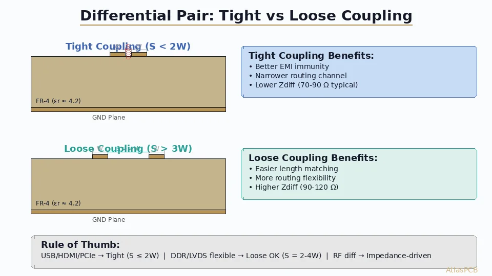
The 3W Rule
Maintain center-to-center spacing of at least 3x the trace width between high-speed signals. This reduces crosstalk to ~5% or less.
For differential pairs: maintain at least 3x the pair width between adjacent pairs (edge-to-edge spacing >= 2x the trace width).
Guard Traces
Ground-connected traces between sensitive signals provide additional isolation. Most effective when connected to ground planes via vias every lambda/20.

Practical Interface Guidelines
DDR3/DDR4 Memory
- Data signals: Length match within byte lane +/-2.5mm (DDR3) or +/-1.0mm (DDR4)
- Address/command: Length match to clock +/-25mm (DDR3) or +/-10mm (DDR4)
- Impedance: 40-60 ohm single-ended (specified by memory controller)
- Routing layer: Stripline preferred for DDR4
- Decoupling: 0.1uF + 0.01uF per VDD pin, placed within 2mm
PCIe Gen3/Gen4
- Differential impedance: 85 ohm +/-10%
- Intra-pair skew: <5 mil (0.13mm)
- Pair-to-pair spacing: >5x trace width
- AC coupling capacitors: 100nF, placed as close to transmitter as possible
- Via transitions: Minimize, use back-drill for stubs >200mil
USB 2.0/3.x
- USB 2.0: 90 ohm differential, max trace length 150mm
- USB 3.0: 85 ohm differential, max trace length 100mm
- Common-mode choke: Recommended near connector for EMI compliance
- Impedance discontinuity at connector: Minimize stub length
Gigabit Ethernet
- 100 ohm differential
- Magnetics placement: <25mm from PHY IC or connector
- Guard ring: Ground pour around Ethernet traces for isolation
- Bob Smith termination: At connector for common-mode noise rejection
Power Delivery Network (PDN)
High-speed ICs require clean, low-impedance power. The PDN must provide current with minimal voltage droop.
Target Impedance
Z_target = V_supply x ripple% / I_max_transient
Example: 1.0V supply, 5% ripple, 2A transient → Z_target = 0.025 ohm
Decoupling Strategy
- Bulk capacitors (100-470uF): Near power entry, handles low-frequency transients
- Mid-range ceramics (1-10uF): Near IC, handles mid-frequency demand
- High-frequency ceramics (0.1uF, 0.01uF): Directly at IC power pins, handles high-frequency noise
- Plane capacitance: Adjacent GND-PWR planes with thin dielectric provide wideband decoupling
Via-to-Pad Connection
- Decoupling capacitor via placement is critical
- Place vias as close to pads as possible (within pad if using via-in-pad)
- Use multiple vias per capacitor pad to reduce via inductance
Layer Transitions and Via Design
Via Stub Problem
When a signal transitions from one layer to another, the unused portion of the through-hole via (the stub) acts as an antenna and causes resonance at:
f_resonance = c / (4 x stub_length x sqrt(Dk))
For a 1.2mm stub in FR-4: f_resonance ≈ 15 GHz. This affects signals above ~7 GHz.
Solutions
- Back-drilling: Remove the unused via stub by controlled-depth drilling from the opposite side. Adds 5-10% to board cost.
- Blind/buried vias: Via only spans the needed layers. No stub.
- Via optimization: Place transitions near the target layer to minimize stub length.
Conclusion
High-speed PCB design is about managing electromagnetic behavior — impedance, return paths, crosstalk, and power delivery. Follow the interface-specific guidelines from IC manufacturers, use field solvers for impedance calculation, simulate critical nets when possible, and work closely with your PCB fabricator on stackup optimization. The fundamentals of controlled impedance, continuous return paths, and proper decoupling apply universally across all high-speed interfaces.
Further Reading
[Via-in-Pad Design: Filled, Capped, and Plated Over — Complete Guide]/blog/via-in-pad-design/)
[Controlled Impedance PCB: Design, Stackup & Testing Explained]/blog/controlled-impedance-pcb/)
[Microstrip vs Stripline: Routing Strategies for Controlled Impedance PCBs]/blog/microstrip-vs-stripline/)
[EMC/EMI Design for PCBs: Passing Compliance on the First Try]/blog/emc-emi-pcb-design/)
[IPC Class 3 Requirements: The Complete Guide for Designers]/blog/ipc-class-3-requirements/)
About AtlasPCB — We specialize in complex PCB manufacturing for HDI, RF, and high-reliability applications. Explore our impedance-controlled PCB manufacturing . Every order includes free engineering review. Get your quote.
Reviewed by AtlasPCB Engineering Team — IPC-certified manufacturing specialists with 15+ years of production experience in HDI, RF, and high-reliability PCB fabrication. Content based on factory floor data and real customer design reviews.
- high-speed design
- signal integrity
- DDR
- PCIe