· AtlasPCB Engineering · Engineering · 10 min read
IPC Class 3 Requirements: The Complete Guide for Designers
Everything PCB designers need to know about IPC Class 3 requirements — acceptability criteria, annular ring, plating thickness, cleanliness, testing, and when Class 3 is actually necessary.
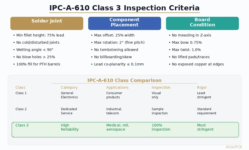
IPC-6012 defines three product classes for rigid printed boards. Class 1 is general electronics. Class 2 is dedicated service electronics — the default for most commercial products. Class 3 is high-reliability electronics — the tightest tolerances, the most documentation, and the highest manufacturing cost.
This guide covers what Class 3 actually requires, when you truly need it, and what it means for your PCB design and manufacturer selection.
The Three IPC Classes at a Glance
| Requirement | Class 1 | Class 2 | Class 3 |
|---|---|---|---|
| Typical use | Consumer, disposable | Commercial, industrial | Military, medical, aerospace |
| Min annular ring (external) | 50μm (2 mil) breakout allowed | 0μm (breakout 90° max) | 25μm (1 mil) min, no breakout |
| Min annular ring (internal) | Breakout 90° allowed | Breakout 180° allowed | Breakout 90° max |
| Min barrel plating | 18μm | 20μm | 25μm |
| Min surface plating | 20μm | 20μm | 25μm |
| Max bow and twist | 1.5% | 1.5% | 0.75% |
| Ionic cleanliness | Not required | Not required | ≤1.56 μg/cm² NaCl equiv. |
| Material traceability | Not required | Recommended | Required |
| Coupon testing | Not required | On request | Required per lot |
Annular Ring: The Most Visible Difference
Annular ring — the copper pad area surrounding a drilled hole — is where Class 2 and Class 3 diverge most visibly.
External Layers
Class 2: Allows tangency (zero annular ring) with breakout up to 90°. The drill hole can touch the edge of the pad — as long as no more than 25% of the hole circumference extends beyond the pad.
Class 3: Requires minimum 1 mil (25μm) annular ring with zero breakout. The drill hole must be completely contained within the pad on every via, on every layer, with at least 1 mil of copper between the hole edge and the pad edge — all the way around.
What This Means for Design
The Class 3 annular ring requirement drives several design constraints:
Larger pads required — If your drill is 0.3mm (12 mil), the minimum pad diameter for Class 3 is 0.3 + 2×(0.025 + registration tolerance) = approximately 0.45mm (18 mil) assuming ±2 mil registration. Class 2 would allow the pad to be the same size as the drill in theory.
Registration budget matters — The 1 mil minimum annular ring means that drill-to-pad misregistration consumes annular ring directly. With ±3 mil registration, you need at least 4 mil annular ring in the design to ensure 1 mil remains after worst-case shift.
BGA fan-out is harder — Fine-pitch BGA escape routing is constrained because pads must be larger relative to vias. This sometimes forces HDI technology earlier than it would be needed under Class 2 rules.
Design rule of thumb for Class 3: Annular ring in your design should be at least (minimum annular ring + registration tolerance + safety margin) = 1 mil + 3 mil + 1 mil = 5 mil minimum design annular ring.
Plating Thickness Requirements
Through-Hole Plating
Class 3 requires minimum 25μm (1 mil) copper plating thickness throughout the via barrel — measured at the thinnest point.
This is a critical reliability parameter. Via barrel plating is the only conductor connecting layers through the board. Under-plated barrels crack during thermal cycling, creating intermittent opens.
What 25μm means in practice:
- The thinnest point in the barrel (usually at the board center for high-aspect-ratio vias) must be ≥25μm
- The manufacturer must plate enough copper at the knee (where the barrel meets the surface) to account for current distribution non-uniformity
- High-aspect-ratio vias (>6:1) are particularly challenging — plating thickness at the center can be 30-50% less than at the ends
Verification: Microsection (cross-section) of plated vias, measured at 3+ locations along the barrel. Class 3 requires coupon testing per production lot.
Surface Plating
Surface copper plating (on external traces and pads) must also meet 25μm minimum. This is measured before any surface finish (ENIG, HASL, etc.) is applied.
Combined with surface finish:
- ENIG: 25μm Cu + 3-5μm Ni + 0.05-0.1μm Au
- HASL: 25μm Cu + 1-25μm Sn/Pb
- OSP: 25μm Cu + 0.2-0.5μm organic
Bow and Twist
Class 3 limit: 0.75% (measured per IPC-TM-650 2.4.22)
This is half the 1.5% limit allowed for Class 1 and Class 2. The tighter limit exists because warped boards cause:
- BGA solder joint opens or shorts during reflow
- Connector mismatch in press-fit applications
- Assembly fixturing problems
- Stress on through-hole components
Achieving 0.75% on complex boards requires:
- Symmetric copper distribution across the stackup
- Balanced dielectric construction
- Controlled lamination parameters (temperature ramp rate, pressure uniformity)
- Copper thieving in low-density areas
- Stress relief after routing (thermal bake)
For high-layer-count boards (16+ layers) with dense copper on outer layers, achieving 0.75% is non-trivial. The manufacturer must actively design the lamination process to control warpage — not just hope for the best.

Cleanliness Requirements
Ionic Contamination
Class 3 limit: ≤1.56 μg/cm² NaCl equivalent (measured per IPC-TM-650 2.3.25)
Ionic contamination on the board surface causes:
- Electrochemical migration (dendritic growth between traces)
- Leakage current between conductors
- Corrosion under environmental stress
The test measures extractable ionic residues by washing the board surface and analyzing the conductivity of the wash solution. The 1.56 μg/cm² limit is stringent — requiring thorough cleaning after every wet process step.
Manufacturing implications:
- Rinse water quality must be monitored (DI water, resistivity >10 MΩ·cm)
- Post-etch, post-plating, and post-solder-mask cleaning steps require validation
- Board storage and handling must prevent recontamination
- Clean room or controlled environment for final inspection and packaging
Visual Inspection
Class 3 tightens visual acceptance criteria across the board:
| Defect | Class 2 Acceptance | Class 3 Acceptance |
|---|---|---|
| Copper void in plating | 5% of length, not in via | Not acceptable |
| Solder mask misregistration | Touches pad OK | Must maintain minimum clearance |
| Conductor width reduction | 20% reduction allowed | 10% reduction maximum |
| Lifted pads | ≤1 per board, repaired | Not acceptable |
| Laminate void | ≤1% of area | ≤0.5% of area |
| Weave exposure | Acceptable if no fibers broken | Not acceptable in functional area |
Testing and Documentation
Required Testing (Class 3)
Microsection — Cross-section of plated vias to verify barrel plating thickness, annular ring, and layer registration. At least 1 coupon per production lot.
Thermal stress — Solder float test (288°C for 10 seconds) on coupons to verify no delamination, blistering, or barrel cracking. Required per IPC-6012 Class 3.
Ionic cleanliness — Extraction and measurement of surface ionic contamination per IPC-TM-650 2.3.25.
Impedance test (if applicable) — TDR measurement on impedance coupons, required for every controlled impedance lot.
Electrical test — 100% continuity and isolation testing of every board.
Required Documentation (Class 3)
| Document | Purpose |
|---|---|
| Material Certificate of Conformance | Traceability to laminate lot, prepreg lot |
| First Article Inspection Report | Dimensional verification of first production board |
| Microsection Report | Via plating thickness and quality |
| Thermal Stress Test Report | Delamination and barrel integrity |
| Impedance Test Report | TDR data (if applicable) |
| Ionic Cleanliness Report | Surface contamination level |
| Electrical Test Report | Continuity/isolation pass/fail |
| Certificate of Conformance | Overall lot acceptance |
This documentation package must accompany every shipment. Not available on request — included as standard.
When You Actually Need Class 3
Class 3 is not free. It costs 20-50% more in fabrication, increases lead time by 2-5 days (additional testing), and constrains your design with tighter annular ring and registration requirements.
You need Class 3 when:
- Human safety depends on the electronics functioning (medical life-support, automotive ASIL C/D, aerospace fly-by-wire)
- Failure causes mission loss (satellite, military deployed systems, deep-sea equipment)
- The product must function after years of storage followed by immediate use (defense, emergency systems)
- Regulatory or contractual requirements specify Class 3 or MIL-PRF-31032
- The operating environment is extreme (wide temperature range, vibration, humidity, altitude)
You probably do not need Class 3 when:
- Consumer electronics, even “premium” consumer products
- IoT devices and sensors (Class 2 is appropriate)
- Telecom infrastructure (Class 2 is standard; some critical path boards may warrant Class 3)
- Industrial controls (Class 2 with enhanced testing is common)
- Prototypes (unless prototypes go directly into qualification testing)
The common mistake: Specifying Class 3 “because we want the best quality” when Class 2 is appropriate. This increases cost and lead time without meaningful reliability improvement for non-critical applications. A well-manufactured Class 2 board from a quality-focused shop is more reliable than a poorly manufactured Class 3 board from a shop that just barely meets the minimum requirements.
Design Checklist for IPC Class 3
Before sending files to a Class 3 manufacturer:
- Annular ring ≥5 mil in design (1 mil minimum + 3 mil registration + 1 mil margin)
- Via aspect ratio within manufacturer’s Class 3 capability (typically ≤8:1)
- Copper distribution balanced for ≤0.75% warpage
- Material grade specified (Tg, Td, specific laminate — not just “FR4”)
- Surface finish specified with Class 3 plating requirements considered
- Class 3 callout on fab drawing (IPC-6012, Class 3)
- All testing requirements listed on fab drawing
- Documentation requirements specified in PO or fab package
How Atlas PCB Handles IPC Class 3
Atlas PCB’s manufacturing partners include IPC Class 3 qualified facilities with documented process capability:
- IPC-6012 Class 3 process — qualified and audited
- Microsection per production lot — barrel plating, annular ring, registration verified
- Thermal stress testing per IPC-TM-650 on every lot
- Ionic cleanliness testing ≤1.56 μg/cm² verified
- Full documentation package with every shipment — material certs, microsection, thermal stress, impedance (if applicable), electrical test
- Material traceability from laminate lot to finished board
- 1-piece minimum — prototype orders receive Class 3 processing and documentation
Every Class 3 order includes 12-hour human engineering pre-audit. Our engineer verifies that your design meets Class 3 annular ring requirements, copper balance supports 0.75% warpage limit, and via structures are compatible with Class 3 plating specifications — before production begins.
Frequently Asked Questions
What is the difference between IPC Class 2 and Class 3?
Class 3 tightens every manufacturing tolerance compared to Class 2. The most impactful differences: minimum 1 mil annular ring with no breakout (Class 2 allows zero annular ring with 90° breakout), 25μm minimum barrel plating (vs 20μm), 0.75% bow and twist limit (vs 1.5%), mandatory ionic cleanliness testing, mandatory microsection per lot, and full material traceability. Class 3 costs 20-50% more but provides measurably higher reliability for applications where failure is not acceptable.
When is IPC Class 3 actually required?
Class 3 is required when the application is safety-critical, mission-critical, or subject to regulatory requirements specifying high-reliability electronics. This includes military and defense systems, aerospace and satellite electronics, medical life-support devices (FDA Class III), safety-critical automotive (ASIL C/D), and nuclear instrumentation. For commercial and industrial products, Class 2 is appropriate and cost-effective. Specifying Class 3 unnecessarily adds cost without proportional reliability improvement.
How much more does IPC Class 3 PCB fabrication cost?
Class 3 adds 20-50% to fabrication cost compared to Class 2, depending on board complexity and the manufacturer’s baseline process. The premium covers tighter process controls (lower yield), additional testing (microsection, thermal stress, ionic cleanliness per lot), documentation requirements, and enhanced inspection criteria. Lead time increases by 2-5 working days due to testing. For prototypes, the percentage premium may be higher because testing costs are amortized over fewer boards.
Summary
- IPC Class 3 requires minimum 1 mil annular ring, 25μm barrel plating, 0.75% bow/twist, and ionic cleanliness testing
- Class 3 costs 20-50% more than Class 2 — justified for safety-critical and mission-critical applications
- Design annular ring ≥5 mil to account for registration tolerance and maintain Class 3 compliance
- Full documentation (microsection, thermal stress, material traceability) must accompany every Class 3 shipment
- Do not specify Class 3 unless the application truly requires it — well-made Class 2 boards are highly reliable for commercial products
Need IPC Class 3 boards from a qualified manufacturer? Upload your Gerbers for a free engineering review — we verify Class 3 design compliance before production. Or talk to an engineer about your reliability requirements.
Related guides: [IPC Standards and PCB Classes]/blog/ipc-standards-pcb-classes/) | [PCB Testing Methods]/blog/pcb-testing-methods/) | [Common PCB Defects and Prevention]/blog/common-pcb-defects-prevention/)
Further Reading
[HDI PCB Design Guide: Stackup Rules, Via Structures & DFM Checklist]/blog/hdi-pcb-design-guide/)
[Controlled Impedance PCB: Design, Stackup & Testing Explained]/blog/controlled-impedance-pcb/)
[PCB Manufacturer with Engineering Review: Why Human DFM Audit Matters]/blog/pcb-manufacturer-engineering-review/)
[ENEPIG vs ENIG: Which PCB Surface Finish for Your Design?]/blog/enepig-vs-enig/)
[PCB Surface Finish Guide: HASL, ENIG, OSP and More Compared]/blog/pcb-surface-finish-guide/)
[PCB DFM Checklist: 50 Points to Review Before Sending Gerbers]/blog/pcb-dfm-checklist/)
[PCB Solder Mask: Types, Colors, and Functions Explained]/blog/pcb-solder-mask-guide/)
[BGA Escape Routing: Strategies for 0.4mm, 0.5mm, and 0.8mm Pitch]/blog/bga-escape-routing/)
[BGA Soldering and Rework: Challenges, Inspection, and Best Practices]/blog/bga-soldering-rework/)
[IPC Class 2 vs Class 3: Which Standard Does Your Board Need?]/blog/ipc-class-2-vs-class-3/)
About AtlasPCB — We specialize in complex PCB manufacturing for HDI, RF, and high-reliability applications. Explore our full PCB manufacturing capabilities . Every order includes free engineering review. Get your quote.
Reviewed by AtlasPCB Engineering Team — IPC-certified manufacturing specialists with 15+ years of production experience in HDI, RF, and high-reliability PCB fabrication. Content based on factory floor data and real customer design reviews.
- IPC Class 3
- high reliability
- pcb quality
- military pcb
- medical pcb