· AtlasPCB Engineering · Engineering · 9 min read
BGA Escape Routing: Strategies for 0.4mm, 0.5mm, and 0.8mm Pitch
Practical guide to BGA escape routing for fine-pitch packages. Covers dog-bone fanout, via-in-pad, layer assignment strategies, and routing channel calculations for 0.4-1.0mm pitch BGAs on 4-12 layer PCBs.
BGA escape routing is where PCB design meets physical reality. The ball grid array’s compact interconnect density is its greatest strength — and the routing challenge is the price you pay for that density.
This guide provides the practical techniques and calculations for escaping signals from BGAs at every common pitch, from 1.0mm commodity packages to 0.4mm high-performance SoCs.
The Escape Problem
A BGA places signals on a 2D grid of solder balls underneath the package. All those signals need to reach other parts of the board. The challenge is extracting (escaping) signals from the interior of the grid to routing channels outside the package footprint.
Key Constraints
- Trace width and spacing must meet manufacturing minimums while fitting between pads
- Via size must be small enough to fit between (or inside) pads
- Number of routing layers must provide enough channels for all interior signals
- Signal integrity requirements constrain trace length and routing topology
The Channel Equation
The number of traces that can pass between two adjacent BGA pads determines how many rows of balls can escape per routing layer:
Channels = floor((Pitch - Pad_Diameter - 2×Clearance) / (Trace_Width + Trace_Space))Escape by Pitch: 1.0mm and 0.8mm
The Comfortable Zone
At 1.0mm and 0.8mm pitch, escape routing is straightforward with standard PCB technology.
1.0mm pitch (typical: 0.5mm pad, 5/5 mil trace/space):
Available gap = 1.0mm - 0.5mm = 0.5mm (19.7mil)
Clearance needed: 2 × 3.5mil = 7mil
Remaining: 12.7mil
Traces: 12.7 / (5+5) = 1.27 → 1 trace between pads
One trace passes between each pair of pads. This means:
- Row 1 (outermost): Escapes directly outward on surface
- Row 2: One trace from Row 3+ passes between Row 1 and 2 pads
- Row 3: Via down to inner routing layer
- Row 4+: Additional routing layers needed
0.8mm pitch (typical: 0.4mm pad, 4/4 mil trace/space):
Available gap = 0.8mm - 0.4mm = 0.4mm (15.7mil)
Clearance needed: 2 × 3mil = 6mil
Remaining: 9.7mil
Traces: 9.7 / (4+4) = 1.21 → 1 trace between pads
Still one trace per channel, but with less margin. Manufacturing tolerance becomes important at this geometry.
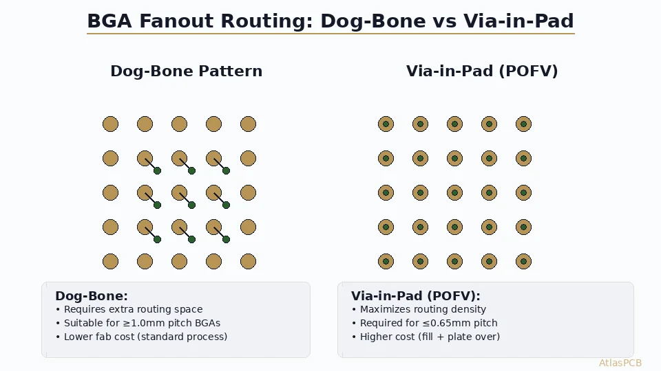
Standard Fanout Pattern (Dog-Bone)
For 0.8mm+ pitch, the standard approach is dog-bone via fanout:
   ○  ○  ○  ○   ← BGA pads (Row 1 - outermost)
   |  |  |  |
   ◎  ◎  ◎  ◎   ← Dog-bone vias (offset from pad)

   ○  ○  ○  ○   ← BGA pads (Row 2)
   |  |  |  |
   ◎  ◎  ◎  ◎   ← Dog-bone vias
Each pad connects to an offset via through a short trace (the “dog-bone neck”). The via drops the signal to an inner layer for routing.
Dog-bone design rules (0.8mm pitch):
- Via pad: 18-20mil
- Via drill: 8-10mil
- Neck width: 4-5mil
- Neck length: 10-15mil
- Via offset direction: alternate between rows to avoid via-to-via clearance violations
Escape at 0.5mm Pitch
The Transition Zone
At 0.5mm pitch, standard dog-bone fanout breaks down for interior rows:
Available gap = 0.5mm - 0.3mm pad = 0.2mm (7.9mil)
Clearance needed: 2 × 3mil = 6mil
Remaining: 1.9mil
Traces: 0 traces between pads
Zero traces can pass between 0.5mm pitch pads using standard design rules. This fundamental geometric constraint drives the requirement for via-in-pad and HDI.
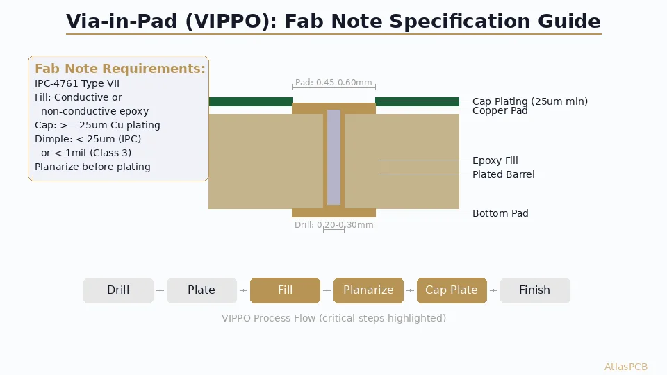
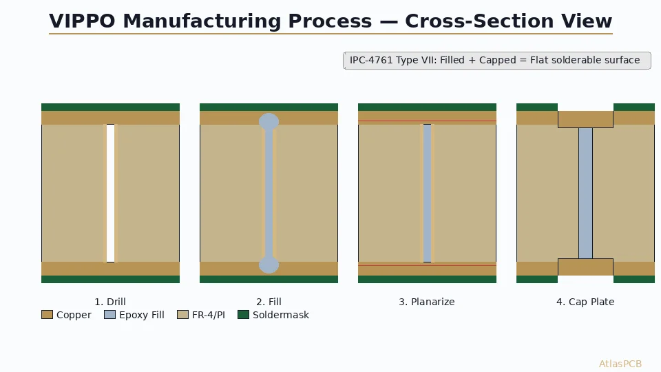
Via-in-Pad Strategy
Via-in-pad eliminates the dog-bone offset, placing the via directly in the BGA pad:
   ⊕  ⊕  ⊕  ⊕   ← BGA pads with via-in-pad (Row 1)

   ⊕  ⊕  ⊕  ⊕   ← BGA pads with via-in-pad (Row 2)
Via-in-pad specifications for 0.5mm pitch:
- Via drill: 8-10mil (0.2-0.25mm)
- Via pad: 12-14mil (0.3-0.35mm) — must fit within BGA pad
- Fill: Conductive or non-conductive epoxy
- Cap plating: Minimum 0.8mil copper over fill
- Surface: Flat — must meet IPC-4761 Type VII (filled and capped)
Layer Assignment for 0.5mm Pitch
With via-in-pad, each inner routing layer can escape 2-3 rows of balls:
| Layer | Rows Escaped | Notes |
|---|---|---|
| L1 (surface) | Rows 1-2 (outermost) | Direct routing outward |
| L3 (inner) | Rows 3-4 | Via from pad to L3, route outward |
| L5 (inner) | Rows 5-6 | Via from pad to L5, route outward |
| L7 (inner) | Rows 7-8 | Via from pad to L7, route outward |
Layer count formula for 0.5mm pitch:
Routing layers needed ≈ ceil(rows_deep / 2)
Total layers ≈ 2 × routing_layers + 2 (for ground/power planes)
A 25×25 ball BGA (0.5mm pitch, 12-13 rows deep from each side) needs approximately 6-7 routing layers → 8-10 total layers.
Escape at 0.4mm Pitch
HDI Territory
At 0.4mm pitch, conventional PCB technology cannot support escape routing. HDI (High Density Interconnect) with microvias and sequential lamination is mandatory.
Available gap = 0.4mm - 0.25mm pad = 0.15mm (5.9mil)
Even with via-in-pad, through-hole vias are too large for the pad
Microvia required: 4mil drill, 8-10mil pad
Microvia Escape Strategy
Stacked microvias connect the surface BGA pad to progressively deeper layers:
L1:  ⊕  ⊕  ⊕  ⊕   ← BGA pads with microvia
     ↓  ↓  ↓  ↓      (microvia L1→L2)
L2:  ●  ●  ●  ●   ← Routing or second microvia
     ↓  ↓  ↓  ↓      (microvia L2→L3)
L3:  ●  ●  ●  ●   ← Routing layer
Stacked microvias allow 3-4 sequential connections from the surface to deep layers. Skip-one-layer microvias (L1→L3) are also available from advanced manufacturers but are more expensive.
HDI design rules for 0.4mm pitch:
| Parameter | Value |
|---|---|
| Microvia drill | 3-4 mil (75-100µm) laser |
| Microvia pad | 8-10 mil (200-250µm) |
| Microvia capture pad | 10-12 mil |
| Trace width | 3-3.5 mil |
| Trace space | 3-3.5 mil |
| Registration tolerance | ±2 mil |
Layer Count for 0.4mm Pitch
Large 0.4mm pitch BGAs (>500 balls) routinely require 10-14 layers with 2-3 sequential lamination cycles:
| Pin Count | Rows Deep | Routing Layers | Total Layers | HDI Build-ups |
|---|---|---|---|---|
| <200 | 6-7 | 4 | 8 | 1+N+1 |
| 200-500 | 8-10 | 5-6 | 10 | 2+N+2 |
| 500-1000 | 12-14 | 7-8 | 12-14 | 2+N+2 or 3+N+3 |
Signal Integrity Considerations
Length Matching in BGA Fanout
For high-speed interfaces (DDR, PCIe, USB), trace lengths must be matched within the BGA escape region. This is challenging because:
- Inner rows have longer escape traces than outer rows
- Signals escaping on different layers have different via stub effects
- The fanout region cannot easily accommodate serpentine length matching
Solutions:
- Pre-plan layer assignments to group length-matched signals on the same escape layer
- Add length compensation outside the BGA footprint (easier to serpentine in open routing channels)
- Use time-domain simulation to account for via transitions rather than relying on physical length matching alone
Via Stub Management
Through-hole vias create stubs that resonate at specific frequencies:
Resonant frequency = c / (4 × stub_length × √Dk)For a standard 62mil board with a signal on L3, the stub extends from L3 to L8 (approximately 50mil). In FR4, the first resonance is at approximately 15GHz.
For signals above 5GHz:
- Back-drill stubs to within 10mil of the signal layer
- Use blind vias that terminate at the target layer
- Use HDI microvias (no stubs by construction)
Power Integrity Under the BGA
A BGA is simultaneously the highest-current-density and highest-switching-speed location on the board. Power delivery to the BGA requires:
- Decoupling capacitors: Place 0201 or 01005 caps within the BGA footprint or immediately adjacent
- Power/ground plane pairs: Dedicate at least one tightly-coupled plane pair in the stackup directly under the BGA
- Via current capacity: Each power/ground via carries a fraction of the total BGA current — verify per-via current does not exceed electromigration limits
Manufacturing Capability Check
Before finalizing your BGA escape design, verify your manufacturer can support the required features:
Capability Matrix
| Feature | Standard PCB | Advanced PCB | HDI |
|---|---|---|---|
| Min drill | 8mil (0.2mm) | 6mil (0.15mm) | 3-4mil laser |
| Min via pad | 16mil | 12mil | 8mil |
| Min trace/space | 4/4mil | 3/3mil | 2.5/2.5mil |
| Via-in-pad fill | No | Yes | Yes |
| Microvias | No | No | Yes (laser) |
| Sequential lamination | No | Limited | Yes |
| Max BGA pitch | 0.8mm+ | 0.5mm | 0.3-0.4mm |
Cost Impact
| Technology | Relative Cost | Typical Application |
|---|---|---|
| Standard PTH | 1× | 0.8mm+ pitch BGA |
| Via-in-pad (filled) | 1.2-1.4× | 0.5mm pitch BGA |
| 1+N+1 HDI | 1.5-2.0× | 0.4mm pitch, low pin count |
| 2+N+2 HDI | 2.0-3.0× | 0.4mm pitch, medium pin count |
| 3+N+3 HDI | 3.0-5.0× | 0.3-0.4mm pitch, high pin count |
Practical Escape Checklist
Before You Start Routing
- Identify BGA pitch and pad size from the component datasheet
- Count signal rows from the outside in (power/ground balls don’t need escape routing — they connect directly to planes via via-in-pad)
- Calculate channels per row using the channel equation
- Determine layer count based on rows requiring escape
- Choose via technology (through-hole, via-in-pad, microvia) based on pitch
- Verify manufacturer capability against your required feature set
During Routing
- Assign layers by row — outermost rows on surface, progressively deeper rows on deeper layers
- Route ground/power balls first — they are simpler (direct via to plane) and constrain signal routing
- Group matched-length signals on the same layer
- Maintain reference plane integrity — avoid splitting ground planes under the BGA
- Check clearances obsessively — DRC violations in the BGA field are the most common escape routing errors
After Routing
- Run DRC with manufacturer-specific rules (not just your default rules)
- Verify via-to-via clearances especially in the BGA field
- Check impedance for controlled-impedance signals in the escape zone
- Simulate critical nets through the via transition (S-parameter or time-domain)
At Atlas PCB, our 12-hour engineering review includes verification of BGA escape routing against our manufacturing capabilities, with specific attention to via-in-pad specifications and HDI build-up requirements.
Frequently Asked Questions
Can I depopulate BGA balls to simplify escape routing?
Yes, if the silicon supports it. Many FPGA and SoC vendors publish recommended ball depopulation patterns that eliminate interior power/ground balls that can be connected through fewer vias. Some application processors have configurable ball maps where unused I/O can be depopulated. Always verify with the component vendor that depopulated balls don’t need to be connected for thermal or electrical reasons. Power balls especially should not be depopulated without thermal analysis.
Should I use non-conductive or conductive fill for via-in-pad?
For most applications, non-conductive epoxy fill is sufficient and less expensive. Conductive fill (copper or silver-filled epoxy) provides lower thermal resistance through the via, which matters for thermal pads under power components. For BGA signal vias, non-conductive fill is standard. For BGA thermal/ground pads where heat transfer through the via is important, conductive fill is preferred. Specify the fill type explicitly in your fabrication notes — don’t leave it to the manufacturer’s default.
How do I handle mixed-pitch BGAs (different pitch in different regions)?
Some packages use finer pitch in the center (where I/O density is highest) and coarser pitch on the perimeter (for power). Design the escape routing for the finest pitch present, then relax rules in coarser regions. The layer count is driven by the finest-pitch region. Use the coarser-pitch perimeter rows for power/ground connections with standard via technology, and reserve the HDI capability for the fine-pitch center.
Further Reading
[HDI PCB Design Guide: Stackup Rules, Via Structures & DFM Checklist]/blog/hdi-pcb-design-guide/)
[HDI PCB Technology: Microvias, Laser Drilling, and High-Density Design]/blog/hdi-pcb-technology/)
[PCB Sequential Lamination: Process, Design Rules, and When You Need It]/blog/pcb-sequential-lamination/)
[Via-in-Pad Design: Filled, Capped, and Plated Over — Complete Guide]/blog/via-in-pad-design/)
[Blind Via vs Buried Via: Design Rules, Cost Impact & When to Use Each]/blog/blind-via-vs-buried-via/)
[High-Speed PCB Design: Signal Integrity Essentials for Modern Electronics]/blog/high-speed-pcb-design/)
[PCB Manufacturer with Engineering Review: Why Human DFM Audit Matters]/blog/pcb-manufacturer-engineering-review/)
[BGA Soldering and Rework: Challenges, Inspection, and Best Practices]/blog/bga-soldering-rework/)
[PCB Pad Design for BGA, QFN, and Passive Components: Best Practices]/blog/pcb-pad-design-bga-qfn/)
[PCB Grounding Techniques: Star, Split, and Solid Ground Plane Strategies]/blog/pcb-grounding-techniques/)
About AtlasPCB — We specialize in complex PCB manufacturing for HDI, RF, and high-reliability applications. Explore our HDI PCB manufacturing capabilities . Every order includes free engineering review. Get your quote.
Reviewed by AtlasPCB Engineering Team — IPC-certified manufacturing specialists with 15+ years of production experience in HDI, RF, and high-reliability PCB fabrication. Content based on factory floor data and real customer design reviews.
- BGA
- escape routing
- pcb design
- via-in-pad
- HDI
- fine pitch