· AtlasPCB Engineering · Engineering · 11 min read
HDI PCB Design Guide: Stackup Rules, Via Structures & DFM Checklist
A practical HDI PCB design guide covering microvia structures, stackup rules, BGA escape routing, via-in-pad design, copper fill requirements, and a complete DFM checklist for HDI boards.
HDI (High Density Interconnect) PCB design enables more functionality in less space — but it requires different design thinking than standard multilayer boards. The rules that work for through-hole vias on 1.6mm FR4 break down when you are routing microvias through 60μm dielectrics.
This guide covers the practical design rules for HDI, from stackup architecture to BGA escape routing to the DFM checklist you should complete before sending files to your manufacturer.
HDI Design Fundamentals
What Makes a Board “HDI”
A PCB qualifies as HDI when it uses one or more of:
- Microvias — laser-drilled vias with diameter ≤150μm (6 mil)
- Blind vias — vias that connect outer layers to inner layers without penetrating the full board
- Sequential buildup — additional layers laminated onto a core in separate press cycles
- Fine lines — trace width/spacing ≤100μm (4 mil)
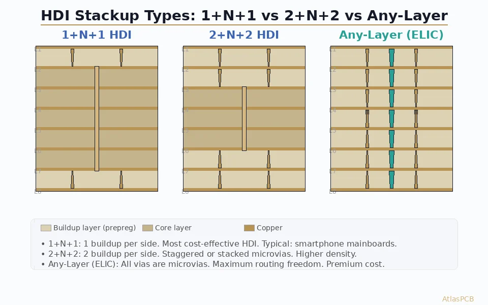
The IPC defines HDI in IPC-2226 using a technology classification system based on via types:
| Type | Description | Via Structure |
|---|---|---|
| Type I | Through vias + blind microvias | 1-N-1 |
| Type II | Through vias + blind + buried microvias | 2-N-2 or similar |
| Type III | Through vias + blind + buried + stacked microvias | 2-N-2 stacked |
| Type IV | Coreless (any-layer) | All microvias, no core |
| Type V | Coreless + stacked microvias | Any-layer stacked |
For most applications, Type I (1-N-1) or Type II (2-N-2) provides sufficient density at reasonable cost.
Stackup Architecture
1-N-1: The Workhorse
One microvia buildup layer on each side of an N-layer core. This is the most common and cost-effective HDI configuration.
L1 — Signal (microvia to L2)     ← Buildup layer
──── Prepreg (60-80μm) ────
L2 — Ground                      ┐
──── Core (100-200μm) ────        │
L3 — Signal                       │ Core
──── Core ────                     │ (standard multilayer)
L4 — Power                        │
──── Core ────                     │
L5 — Signal                       │
──── Core ────                    ┘
L6 — Ground
──── Prepreg (60-80μm) ────
L7 — Signal (microvia to L6)     ← Buildup layer
When to use 1-N-1:
- BGA pitch 0.65-0.8mm where through-hole fan-out is possible but wasteful
- Moderate density increase needed (20-30% more routing vs standard)
- Cost sensitivity — 1-N-1 adds only 30-40% to board cost
Design rules for 1-N-1:
- Microvias span only L1→L2 and LN-1→LN
- Core layers use standard through-hole vias
- L1/L2 and LN-1/LN connection is via microvia; L1-to-L3+ requires microvia + through-hole via
2-N-2: Higher Density
Two buildup layers on each side. Microvias can be staggered or stacked.
L1 — Signal (microvia to L2)           ← Buildup 2
──── Prepreg (60μm) ────
L2 — Signal/Ground (microvia to L1,L3) ← Buildup 1
──── Prepreg (60μm) ────
L3 — Ground                            ┐
──── Core ────                           │ Core
L4 — Power                              │
──── Core ────                          ┘
L5 — Ground
──── Prepreg (60μm) ────
L6 — Signal/Ground                     ← Buildup 1
──── Prepreg (60μm) ────
L7 — Signal (microvia to L6)           ← Buildup 2
Staggered vs. Stacked:
| Aspect | Staggered | Stacked |
|---|---|---|
| Via alignment | Offset between layers | Directly on top |
| Fill requirement | No fill required | Copper fill mandatory |
| Routing flexibility | Lower — offset consumes space | Higher — vertical connection |
| Reliability | Good | Good (when properly filled) |
| Manufacturing difficulty | Moderate | Higher |
| Cost premium | +50-70% vs standard | +70-100% vs standard |
When to use stacked: When you need direct L1→L3 vertical connection (e.g., escaping a 0.4mm pitch BGA to L3 ground plane) and cannot route laterally on L2 to reach a staggered via.
When staggered is fine: When L2 has enough routing space to reach an offset via position, and the lateral routing does not create signal integrity issues.
Any-Layer: Maximum Density
No core. Every layer pair connected by microvias. Any signal on any layer can connect to any adjacent layer.
When to use any-layer:
- Ultra-fine-pitch components (≤0.3mm BGA pitch)
- Extreme density requirements (smartphones, advanced SiP substrates)
- Layer count reduction is paramount (replacing 16+ layer standard with 8-layer any-layer)
Practical considerations:
- Cost: 2-3x standard multilayer
- Lead time: 2-4 weeks longer than standard
- Manufacturer capability: Only Tier 1 HDI shops
- Design complexity: Requires careful planning of via stack structures
BGA Escape Routing
BGA escape routing is the most common reason designs need HDI. Here is how to approach it systematically.
Pitch-Based Strategy
| BGA Pitch | Recommended Via Strategy |
|---|---|
| ≥1.0mm | Through-hole via between pads — HDI not needed |
| 0.8mm | Through-hole via between pads (tight) or via-in-pad (preferred) |
| 0.65mm | 1-N-1 HDI with via-in-pad on L1→L2 |
| 0.5mm | 1-N-1 or 2-N-2 HDI with via-in-pad |
| 0.4mm | 2-N-2 HDI with stacked microvias |
| ≤0.3mm | Any-layer HDI |
Via-in-Pad Design
Via-in-pad places the microvia directly in the BGA pad, eliminating the need for dog-bone fan-out routing. This saves space and improves signal integrity.
Requirements for via-in-pad:
- Via must be filled (copper or conductive paste) and planarized
- Surface planarity: ≤15μm dimple or protrusion per IPC-4761 Type VII
- The filled via becomes a solderable surface — must be flat enough for reliable BGA attachment
Design rules for via-in-pad with microvias:
- Microvia diameter: 100-125μm
- Pad diameter: 250-300μm (for 0.5mm pitch BGA with 270μm pad)
- Via-to-pad centering tolerance: ±50μm
- Fill specification: “Copper filled and planarized, Type VII per IPC-4761”
Call this out explicitly on your fab drawing. Do not assume the manufacturer will fill and planarize. State: “All vias in BGA pads shall be copper-filled and planarized per IPC-4761 Type VII.”
Escape Routing Pattern
For a BGA with via-in-pad on a 1-N-1 HDI:
- Outer two rows — Escape directly via microvia from L1 to L2, route on L2
- Inner rows — Microvia to L2, then through-hole via to inner layers for routing
- Center pins — May require routing on L2 to reach a through-hole via position
For 2-N-2 with stacked microvias:
- Outer rows — Microvia L1→L2, route on L2 or via to L3
- Inner rows — Stacked microvia L1→L2→L3, route on L3
- Core through-hole vias accessible from L3 for connections to deeper layers
The key principle: each buildup layer provides one additional “escape row” from the BGA center.
Impedance Control on HDI Layers
HDI buildup layers use thin dielectrics (40-80μm), which changes impedance behavior:
Microstrip on Buildup Layer
For a 50Ω microstrip on L1 with L2 as reference:
- Dielectric height: 60μm (typical buildup prepreg)
- Dk: 3.8-4.2 (depends on prepreg)
- Required trace width: ~55-65μm (2.2-2.6 mil)
These are much narrower traces than standard PCB design. Verify that your manufacturer can reliably etch and plate traces at this width — minimum production-capable line width for most HDI shops is 50-75μm.
Solder Mask Impact
On L1 microstrip, solder mask adds to the effective dielectric, increasing impedance by 1-5Ω depending on mask thickness. The manufacturer’s field solver should include solder mask in the impedance model.
Stripline in Core
Core layers in an HDI board use the same impedance design rules as standard multilayer. The core dielectric is well-controlled, making stripline impedance more predictable than microstrip on thin buildup layers.
Design recommendation: Place your most impedance-critical traces on core stripline layers (better Dk uniformity) rather than on buildup microstrip layers (thinner dielectric, more variability).
Via Reliability: What the Specs Require
Microvia reliability is determined by the copper plating quality and the via geometry. Key reliability factors:
Microvia Aspect Ratio
Maximum recommended: 1:1 (via depth equal to via diameter)
For a 100μm microvia through a 75μm dielectric, the aspect ratio is 0.75:1 — well within limits. For a 75μm microvia through a 100μm dielectric, the ratio is 1.33:1 — marginal and manufacturer-dependent.
Stacked Microvia Reliability
Stacked microvias are the highest-risk structure in HDI design. Failure mechanism: the interface between stacked vias can crack during thermal cycling if:
- The lower via is not completely copper-filled (void acts as stress concentrator)
- CTE mismatch between fill material and surrounding copper creates strain
- The via stack passes through a material boundary (e.g., buildup to core interface)
Reliability rules for stacked microvias:
- Copper fill ≥95% (verified by cross-section)
- Maximum 3 stack levels for production reliability
- IST qualification testing for new stack configurations
- Avoid stacking across material boundaries (e.g., across a core-to-buildup interface)
IPC-4761 Via Fill Types
| Type | Description | Application |
|---|---|---|
| Type I | Tented via (solder mask over) | Standard, non-BGA areas |
| Type II | Tented and covered (mask both sides) | Non-functional vias |
| Type V | Filled and covered (non-conductive fill + mask) | BGA via-in-pad (non-stacked) |
| Type VI | Filled and capped (metal capped) | Medium reliability stacking |
| Type VII | Filled and planarized (copper-filled, flat) | BGA via-in-pad, stacked microvias |
For stacked microvias and BGA via-in-pad, always specify Type VII.
HDI DFM Checklist
Complete this checklist before sending HDI files to your manufacturer:
Via Design
- Microvia diameter ≥75μm (≥100μm preferred for cost/yield)
- Microvia aspect ratio ≤1:1
- Microvia capture pad ≥ drill + 100μm (50μm annular ring per side)
- Stacked microvias: copper fill specified (Type VII per IPC-4761)
- Stacked depth ≤3 levels
- Via-in-pad: fill and planarize specified in fab notes
- Back-drill specified with target stub length (if applicable)
Stackup
- Stackup reviewed with manufacturer for material availability
- Buildup dielectric thickness matches available prepreg
- Stackup is symmetric around center (prevents warpage)
- Signal layers have adjacent reference planes
- Total thickness within manufacturer’s press capability
Routing
- Trace width meets manufacturer’s minimum for the copper weight
- Trace width/spacing confirmed for target impedance on thin dielectrics
- BGA escape routing verified (enough layers for complete escape)
- No traces routed under BGA without confirming solderable surface
Documentation
- HDI structure clearly specified: “1-N-1” or “2-N-2” etc.
- Via fill type specified per IPC-4761 (Type VII for stacked/via-in-pad)
- Impedance targets per layer with tolerance
- Cross-section and microsection requirements stated
- Stackup drawing included (not just a layer count)
Common HDI Design Mistakes
Mistake 1: Microvia on Thick Dielectric
Specifying a 75μm microvia through a 150μm dielectric (aspect ratio 2:1). The laser drill cannot cleanly form this geometry, and plating uniformity degrades.
Fix: Either increase microvia diameter to 150μm or reduce dielectric thickness to ≤75μm.
Mistake 2: Unfilled Stacked Microvias
Designing stacked microvias without specifying copper fill. The manufacturer may stack unfilled vias, creating a void at the interface that becomes a reliability time bomb.
Fix: Add explicit note: “All stacked microvias shall be copper-filled and planarized per IPC-4761 Type VII.”
Mistake 3: Asymmetric HDI Stackup
Designing a 1-0-N stackup (one buildup on top, none on bottom) for a dense top-side design. The asymmetry causes warpage.
Fix: Use symmetric construction (1-N-1) even if only one side needs HDI. The opposite buildup layer can serve as a routing or ground layer.
Mistake 4: Impedance Calculation with Wrong Dk
Using standard FR4 Dk (4.2) for HDI buildup prepreg. HDI prepregs are thin, high-resin-content materials with Dk ranging from 3.5-4.0.
Fix: Get the actual Dk from your manufacturer for the specific prepreg they will use. Simulate impedance with that value.
Mistake 5: No Stackup Discussion with Manufacturer
Designing the stackup in isolation and sending it as a fixed requirement. The manufacturer may not have the exact prepreg thicknesses specified, forcing substitutions that affect impedance.
Fix: Share your draft stackup with the manufacturer early. They will map it to available materials and confirm impedance feasibility before you finalize routing.
How Atlas PCB Handles HDI Design Support
Atlas PCB provides engineering support throughout the HDI design process:
- Pre-design consultation — Share your BGA map and density requirements; we recommend the optimal HDI configuration (1-N-1, 2-N-2, any-layer) based on cost-performance trade-off
- Stackup optimization — We map your target stackup to available materials and simulate impedance before you finalize routing
- DFM review — 12-hour human engineering review of via structures, aspect ratios, fill specifications, and routing feasibility
- Manufacturing capability — 1-N-1, 2-N-2, and 3-N-3 HDI in production, 75μm minimum microvia, copper fill Type VII
- Minimum order — 1 piece, full engineering review included
Frequently Asked Questions
What is the minimum via size for HDI PCBs?
Production-proven minimum microvia sizes are 75-100μm for CO2 laser and 25-50μm for UV-YAG laser. The manufacturing sweet spot is 100μm diameter with 250μm pad — this combination offers reliable yield at reasonable cost from most HDI-capable manufacturers. Going below 75μm requires UV laser capability and increases cost. Design at 100μm unless density analysis proves you need smaller.
When do I need HDI instead of standard multilayer?
The clearest indicator is BGA pitch: at ≤0.8mm pitch, HDI via-in-pad is typically more efficient than through-hole dog-bone fan-out. Other triggers: standard multilayer design requires 4+ additional layers just for routing density, via stubs degrade signal integrity above 5GHz, or board size is constrained. Calculate the cost of HDI with fewer layers vs. standard multilayer with more layers — HDI often wins when it saves 2+ layers.
What is the maximum number of stacked microvias?
Most manufacturers reliably produce 2-3 stacked levels. Beyond 3 levels, reliability risk increases significantly — the cumulative stress at via interfaces during thermal cycling becomes difficult to manage. All stacked microvias must be copper-filled (IPC-4761 Type VII). If your design needs connections spanning more than 3 buildup layers, use a combination of stacked microvias to reach the core, then a core through-hole via, then stacked microvias on the opposite side.
Summary
- 1-N-1 HDI is the most cost-effective density upgrade; use it when BGA pitch hits ≤0.8mm
- 2-N-2 with stacked microvias for ≤0.5mm pitch; any-layer for ≤0.3mm pitch
- Maintain microvia aspect ratio ≤1:1 and always specify copper fill for stacked structures
- Via-in-pad requires explicit Type VII fill-and-planarize callout on your fab drawing
- Discuss stackup with your manufacturer before finalizing routing — material availability drives the design
- Symmetric stackup construction is mandatory for warpage control
Ready to start your HDI design? Upload your Gerbers for a free engineering review, or talk to an engineer early in your design process to optimize your HDI stackup.
Related guides: [HDI PCB Manufacturer]/blog/hdi-pcb-manufacturer/) | [Blind Via vs Buried Via]/blog/blind-via-vs-buried-via/) | [PCB Via Types Guide]/blog/pcb-via-types-guide/)
Further Reading
[HDI PCB Technology: Microvias, Laser Drilling, and High-Density Design]/blog/hdi-pcb-technology/)
[How to Design an HDI Stackup: Step-by-Step for First-Time Designers]/blog/how-to-design-hdi-stackup/)
[Via-in-Pad Design: Filled, Capped, and Plated Over — Complete Guide]/blog/via-in-pad-design/)
[Microstrip vs Stripline: Routing Strategies for Controlled Impedance PCBs]/blog/microstrip-vs-stripline/)
[High-Speed PCB Design: Signal Integrity Essentials for Modern Electronics]/blog/high-speed-pcb-design/)
[Controlled Impedance PCB: Design, Stackup & Testing Explained]/blog/controlled-impedance-pcb/)
[PCB DFM Checklist: 50 Points to Review Before Sending Gerbers]/blog/pcb-dfm-checklist/)
[PCB Manufacturer with Engineering Review: Why Human DFM Audit Matters]/blog/pcb-manufacturer-engineering-review/)
[PCB Solder Mask: Types, Colors, and Functions Explained]/blog/pcb-solder-mask-guide/)
[BGA Escape Routing: Strategies for 0.4mm, 0.5mm, and 0.8mm Pitch]/blog/bga-escape-routing/)
About AtlasPCB — We specialize in complex PCB manufacturing for HDI, RF, and high-reliability applications. Explore our HDI PCB manufacturing capabilities, or get an multilayer PCB fabrication up to 30 layers . Every order includes free engineering review. Get your quote.
Reviewed by AtlasPCB Engineering Team — IPC-certified manufacturing specialists with 15+ years of production experience in HDI, RF, and high-reliability PCB fabrication. Content based on factory floor data and real customer design reviews.
- HDI
- microvia
- pcb design
- BGA routing
- via in pad
- stackup design