· AtlasPCB Engineering · Engineering · 10 min read
HDI PCB Manufacturer: How to Choose the Right Partner for Complex Boards
A practical guide to evaluating HDI PCB manufacturers. Covers microvia capability, sequential lamination, laser drill specs, and what separates reliable suppliers from the rest.
When your design has BGA components with pitch below 0.8mm, routing channels that standard vias cannot support, or board size constraints that demand higher density — you need HDI. And you need a manufacturer who does HDI as a core competency, not an afterthought.
This guide explains what to evaluate when choosing an HDI PCB manufacturer, what questions to ask, and what red flags to watch for.
When Standard PCBs Are Not Enough
Standard multilayer PCBs use mechanical drilling for through-hole vias — typically 0.2mm (8 mil) minimum diameter. These vias consume routing space on every layer they pass through, whether that layer uses the connection or not.
HDI technology solves this with microvias, blind vias, and buildup layer construction. The result: more routing density in fewer layers.
You need HDI when:
- Your design includes BGA packages with ≤0.8mm pitch (0.5mm pitch almost always requires HDI)
- Standard fan-out routing cannot escape a BGA in the available area
- Board size is constrained and you cannot add layers to gain routing channels
- Signal integrity requirements demand shorter via stubs (microvias have negligible stub length)
- Your competitor’s product is smaller than yours and you need to match the form factor
HDI Classification: 1-N-1, 2-N-2, and Any-Layer
Understanding HDI classification is essential for specifying your board and evaluating manufacturer capability.
1-N-1 (Type II HDI)
One buildup layer on each side of an N-layer core. Microvias connect layer 1 to layer 2 and layer N-1 to layer N. The core layers use conventional through-hole vias.
Manufacturing complexity: Low-to-moderate. One additional lamination cycle per side. Most HDI-capable manufacturers handle this reliably.
Typical application: Smartphones, tablets, compact IoT devices. Enables BGA escape routing that through-hole vias cannot achieve.
2-N-2 (Type III HDI)
Two buildup layers on each side. This introduces a choice between staggered microvias (offset between layers) and stacked microvias (directly on top of each other).
| Via Structure | Manufacturing | Reliability | Routing Flexibility |
|---|---|---|---|
| Staggered | Easier — no fill required | Good — stress distributed | Moderate — offset reduces escape options |
| Stacked (copper-filled) | Harder — requires via fill + planarization | Excellent when filled properly | Maximum — direct vertical connections |
Stacked microvias require copper filling. Unfilled stacked vias are a reliability risk — the void inside the lower via creates a stress concentration point during thermal cycling. If your manufacturer claims to do stacked microvias but does not copper-fill them, walk away.
Any-Layer HDI
No core. Every layer is a buildup layer with microvias connecting any two adjacent layers. This provides maximum routing density — vias can be placed under any BGA pad on any layer without consuming routing channels on other layers.
Manufacturing complexity: Very high. Requires multiple sequential lamination cycles (one per layer pair), copper-filled vias at every level, and extremely tight registration.
Typical application: Leading-edge smartphones, wearables, advanced SiP (System-in-Package) substrates.
Not every HDI manufacturer can do any-layer. This capability requires investment in equipment and process development. Verify with production samples, not marketing claims.
7 Things to Verify Before Placing an HDI Order
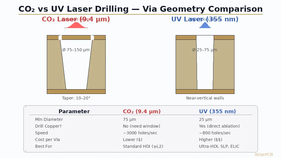
1. Laser Drill Capability
HDI microvias are drilled by laser — either CO2 or UV-YAG. The type of laser determines the minimum via size, material compatibility, and throughput.
| Parameter | CO2 Laser | UV-YAG Laser |
|---|---|---|
| Minimum via diameter | 75-100μm | 25-50μm |
| Drills through copper? | No — requires window opening | Yes — direct copper ablation |
| Speed | Fast (high throughput) | Slower per via |
| Material compatibility | Standard FR4, some RF laminates | All dielectrics including thin films |
| Typical application | 1-N-1 and 2-N-2 HDI | Any-layer, ultra-fine pitch, substrate-like |
Ask: “What laser type do you use? What is your minimum production-proven via size?” The answer should be specific — “75μm production-proven, 50μm in qualification” — not “we can do small vias.”
2. Sequential Lamination and Registration
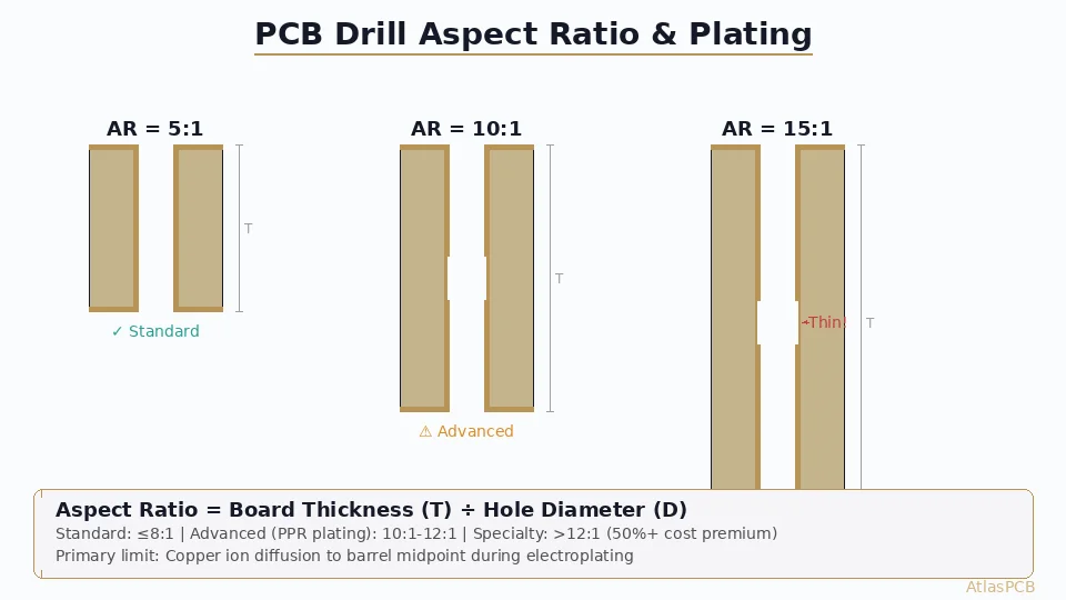
Each buildup layer requires a separate lamination cycle. A 2-N-2 board has at least 4 lamination cycles (core + 2 buildup on each side). Registration error accumulates.
Critical metric: Layer-to-layer registration after all lamination cycles. For HDI, you need ±25-50μm (±1-2 mil) to maintain annular ring on microvias.
Verification: Request cross-section photos from a recent HDI production run showing via-to-pad alignment. If they cannot provide this, they do not have a controlled process.
3. Via Fill and Planarization
For stacked microvias and via-in-pad designs, the manufacturer must fill vias with copper or conductive paste, then planarize the surface for the next buildup layer.
Copper-filled vias provide the best electrical and thermal performance and are required for stacked structures. The fill process must achieve ≥95% fill (measured by cross-section) with no voids.
Surface planarity after filling should be ≤15μm dimple/protrusion per IPC-4761 Type VII. Poor planarity causes solder paste bridging and opens during component assembly.
4. Via Reliability Testing
HDI microvias are smaller and thinner than through-hole vias, making them more susceptible to thermal fatigue. Reliable manufacturers test via integrity using:
- IST (Interconnect Stress Testing) — accelerated thermal cycling using internal resistance heating. IPC-TM-650 2.6.26 standard.
- Thermal cycling — 500-1000 cycles from -55°C to +125°C per IPC-6012 Class 3.
- Microsection analysis — cross-section inspection of via barrel plating thickness, via fill quality, and interface integrity.
Ask: “Do you perform IST or thermal cycling on HDI production lots? What is your pass/fail criteria?” Any manufacturer doing serious HDI work will have data.
5. Line Width and Space Capability
HDI boards often need fine lines to route between BGA pads. Verify the manufacturer’s production-capable (not theoretical) minimum line/space:
| HDI Order | Typical Min Line/Space | Advanced |
|---|---|---|
| 1-N-1 | 75/75μm (3/3 mil) | 50/50μm |
| 2-N-2 | 75/75μm (3/3 mil) | 50/50μm |
| Any-layer | 50/50μm (2/2 mil) | 30/30μm |
Production-capable means they run this spec routinely with acceptable yield — not that they made one sample once. Ask for their yield rate at the specified line/space.
6. Material Selection for HDI
HDI stackups use thin prepregs and cores for buildup layers — typically 40-100μm dielectric between copper layers. Material selection affects:
- Laser drill quality — some resins drill cleaner than others under CO2 laser
- Dielectric constant stability — critical for impedance control on thin dielectrics
- CTE matching — z-axis CTE mismatch between core and buildup causes via stress
Common HDI materials:
- Standard: Shengyi S1000-2, ITEQ IT-180A (adequate for 1-N-1)
- Mid-range: Panasonic Megtron 4 (low Df for high-speed, good HDI processability)
- Premium: Panasonic Megtron 6, Isola I-Speed (very low loss, any-layer HDI)
For most HDI applications below 10GHz, standard high-Tg FR4 works fine. Do not over-specify materials — it adds cost without benefit if your signals do not demand it.
7. Engineering Review and DFM Feedback
HDI designs have more ways to fail in manufacturing than standard multilayer boards. A proper engineering review should catch:
- Microvia aspect ratio violations (laser via in too-thick dielectric)
- Via-in-pad without fill specification (will cause solder voiding)
- Stacked via without copper fill (reliability risk)
- Fine-line routing in areas with poor copper balance (etching uniformity issue)
- Impedance targets incompatible with the specified stackup
Red flag: If a manufacturer accepts your HDI Gerbers without a single question or DFM comment, they are either very experienced with your exact design — or they are not reviewing the files at all. The second case is far more common.
Typical HDI Stackup Configurations
1+6+1 (8-layer, 1-N-1)
The most common HDI configuration. One microvia layer on each side of a 6-layer core.
L1 — Signal (microvia to L2)
L2 — Ground
L3 — Signal (through-hole vias)
L4 — Power
L5 — Signal
L6 — Ground
L7 — Signal
L8 — Signal (microvia to L7)
Cost premium over standard 8-layer: ~30-40%. Significant density improvement for BGA escape routing.
2+4+2 (8-layer, 2-N-2)
Two buildup layers on each side of a 4-layer core. Enables stacked microvias from L1 to L3.
L1 — Signal (stacked microvia L1→L2→L3)
L2 — Signal/Ground (microvia to L1 and L3)
L3 — Ground
L4 — Power
L5 — Ground
L6 — Signal/Ground
L7 — Signal
L8 — Signal
Cost premium over standard 8-layer: ~60-80%. Required for 0.4mm pitch BGA with full fan-out.
Any-Layer 8L
No core. All 8 layers connected by microvias. Any pad on any layer can connect to any adjacent layer.
Cost premium over standard 8-layer: ~100-150%. Used when density requirements cannot be met any other way.
For more on HDI stackup planning, see our [HDI PCB technology guide]/blog/hdi-pcb-technology/).
Common HDI Manufacturing Defects
Understanding failure modes helps you evaluate whether a manufacturer’s process controls are adequate.
| Defect | Cause | Prevention |
|---|---|---|
| Microvia barrel crack | Insufficient plating thickness, CTE mismatch | 20μm+ plating, IST qualification |
| Via fill void | Incomplete copper fill, trapped chemistry | Cross-section inspection, >95% fill spec |
| Pad cratering | Excessive drill energy, weak resin-glass interface | Laser parameter optimization, material selection |
| Registration failure | Accumulated lamination error | Optical registration, X-ray verification |
| Impedance drift | Thin dielectric tolerance variation | Field solver modeling, TDR verification |
| Delamination | Moisture absorption, insufficient cure | Baking before lamination, cure monitoring |
How Atlas PCB Handles HDI
Atlas PCB partners with manufacturers whose primary business includes HDI production — not manufacturers who occasionally accept an HDI order.
- HDI orders: 1-N-1, 2-N-2, and 3-N-3 in production. Any-layer available for qualified designs.
- Microvia: Minimum 75μm laser-drilled, copper-filled for stacked structures
- Registration: ±25μm layer-to-layer on buildup layers
- Line/space: 50/50μm production-capable on inner layers
- Via fill: Copper-filled with ≤15μm dimple per IPC-4761 Type VII
- Testing: IST qualification on new stackup configurations
- Minimum order: 1 piece — same engineering review as a 1000-piece production order
Every HDI order includes a 12-hour human engineering pre-audit. Our CAM engineer reviews your microvia stack structure, aspect ratios, impedance feasibility on the proposed stackup, and via reliability risks before production begins. If anything does not work, we contact you directly.
Frequently Asked Questions
What makes a manufacturer qualified for HDI PCBs?
A qualified HDI manufacturer needs UV or CO2 laser drilling equipment for microvias under 150μm, sequential lamination presses with optical registration, copper-filled via capability for stacked structures, and process controls for via reliability testing (IST or thermal cycling). Do not rely on website claims alone — ask for their minimum via size in production (not R&D), maximum buildup order with production yield data, and cross-section photos from recent HDI lots.
What is the difference between 1-N-1, 2-N-2, and any-layer HDI?
1-N-1 has one buildup layer on each side of an N-layer core — microvias connect only the outermost layer to the layer beneath it. 2-N-2 adds a second buildup layer with staggered or stacked microvias, enabling connections spanning two buildup layers. Any-layer HDI eliminates the core entirely, allowing microvia connections between any two adjacent layers throughout the entire stackup. Each step up significantly increases manufacturing complexity and cost.
How much more does HDI cost compared to standard multilayer PCBs?
HDI boards typically cost 30-80% more than an equivalent-density standard multilayer board, depending on the HDI order and via structure. The premium covers laser drilling, sequential lamination cycles, copper via filling, and tighter process controls. However, HDI frequently reduces total layer count — a 12-layer standard board may be replaced by an 8-layer 1-N-1 HDI — partially offsetting the per-layer cost increase. For most BGA-heavy designs, the trade-off favors HDI.
Summary
- HDI is required when BGA pitch drops below 0.8mm or routing density exceeds through-hole via limits
- Evaluate manufacturers on laser drill capability, sequential lamination registration, and via fill quality — not just “we do HDI”
- Stacked microvias must be copper-filled; accept no alternatives
- Request IST or thermal cycling data and cross-section photos from recent production
- HDI adds cost per layer but often reduces total layer count, making the net cost impact smaller than expected
Ready to get your HDI board manufactured right? Upload your Gerbers for a free engineering review, or talk to an engineer about your HDI stackup requirements.
Related guides: [HDI PCB Technology]/blog/hdi-pcb-technology/) | [PCB Via Types Guide]/blog/pcb-via-types-guide/) | [PCB Stackup Design Guide]/blog/pcb-stackup-design-guide/)
Further Reading
[HDI PCB Design Guide: Stackup Rules, Via Structures & DFM Checklist]/blog/hdi-pcb-design-guide/)
[PCB Sequential Lamination: Process, Design Rules, and When You Need It]/blog/pcb-sequential-lamination/)
[How to Design an HDI Stackup: Step-by-Step for First-Time Designers]/blog/how-to-design-hdi-stackup/)
[Via-in-Pad Design: Filled, Capped, and Plated Over — Complete Guide]/blog/via-in-pad-design/)
[Blind Via vs Buried Via: Design Rules, Cost Impact & When to Use Each]/blog/blind-via-vs-buried-via/)
[High-Speed PCB Design: Signal Integrity Essentials for Modern Electronics]/blog/high-speed-pcb-design/)
[High-Multilayer FR4 vs Standard FR4: When to Upgrade Material Grade]/blog/high-multilayer-fr4-vs-standard-fr4/)
[Multilayer PCB Stackup Design Guide: 8 to 30+ Layers Step by Step]/blog/multilayer-pcb-stackup-design-guide/)
[PCB DFM Checklist: 50 Points to Review Before Sending Gerbers]/blog/pcb-dfm-checklist/)
[PCB Manufacturer with Engineering Review: Why Human DFM Audit Matters]/blog/pcb-manufacturer-engineering-review/)
About AtlasPCB — We specialize in complex PCB manufacturing for HDI, RF, and high-reliability applications. Explore our HDI PCB manufacturing capabilities . Every order includes free engineering review. Get your quote.
Reviewed by AtlasPCB Engineering Team — IPC-certified manufacturing specialists with 15+ years of production experience in HDI, RF, and high-reliability PCB fabrication. Content based on factory floor data and real customer design reviews.
- HDI
- microvia
- pcb manufacturer
- high density interconnect
- laser drilling