· AtlasPCB Engineering · Engineering · 9 min read
How to Design an HDI Stackup: Step-by-Step for First-Time Designers
A step-by-step guide to designing your first HDI PCB stackup. Covers HDI order selection, microvia planning, sub-lamination structure, impedance considerations, and common mistakes.
Your first HDI design is always harder than it should be. Standard PCB stackup rules still apply, but HDI adds new variables: microvia layers, sequential lamination sequence, via stacking rules, and buildup dielectric constraints.
This guide walks through HDI stackup design step by step — from determining whether you need HDI at all, through selecting the right HDI order, to building and validating a complete stackup.
Step 1: Determine If You Need HDI
Before investing in an HDI stackup, confirm that standard through-hole technology cannot meet your requirements.
You need HDI when:
| Indicator | Standard PCB | HDI Required |
|---|---|---|
| BGA pitch | ≥0.8mm | <0.8mm |
| BGA pin count | <400 pins | 400+ pins on a single BGA |
| Via size in BGA field | 0.3mm drill fits between pads | Via too large for pad-to-pad spacing |
| Routing channels | Enough space between vias | No routing channels between through-hole vias |
| Board area | Flexible | Constrained — cannot increase board size |
| Via stub length | Acceptable for signal speed | Stubs cause signal integrity issues (>5GHz) |
If none of these apply, standard multilayer with through-hole vias is cheaper and simpler. Do not use HDI unless you need it.
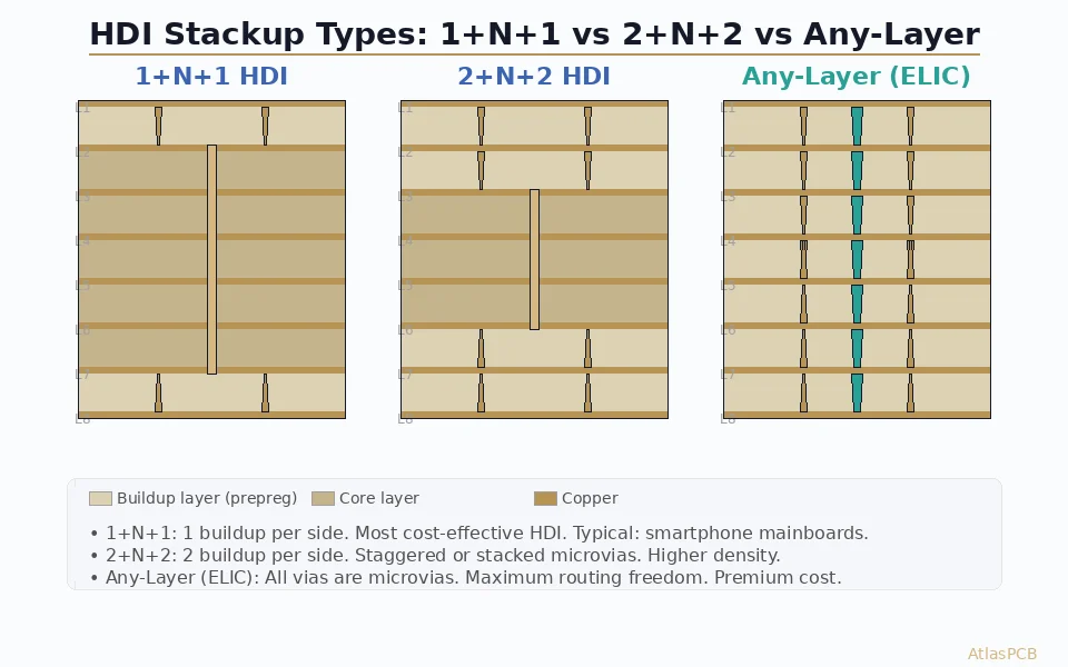
Step 2: Select the HDI Order
The “HDI order” describes how many buildup layers are on each side of the core.
1-N-1: One Buildup Layer Per Side
Structure: 1 microvia layer + N core layers + 1 microvia layer
When to use:
- BGA pitch 0.65-0.8mm
- One level of microvia escape is sufficient
- Moderate routing density improvement is needed
Example: 1+6+1 = 8 layers total
L1 (buildup) — μvia to L2
L2 (core top)
L3 (core)
L4 (core)
L5 (core)
L6 (core)
L7 (core bottom)
L8 (buildup) — μvia to L7
Manufacturing impact: One additional lamination cycle per side (2 total). Adds approximately 30-40% to cost vs standard 8-layer.
2-N-2: Two Buildup Layers Per Side
Structure: 2 microvia layers + N core layers + 2 microvia layers
When to use:
- BGA pitch 0.4-0.5mm
- Two levels of microvia escape needed for full BGA fan-out
- Higher routing density required
Example: 2+4+2 = 8 layers total
L1 (buildup 2) — μvia to L2
L2 (buildup 1) — μvia to L1 and L3
L3 (core top)
L4 (core)
L5 (core)
L6 (core bottom)
L7 (buildup 1) — μvia to L6 and L8
L8 (buildup 2) — μvia to L7
Via structure decision: Staggered or stacked microvias between buildup layers.
- Staggered: L1→L2 microvia is offset from L2→L3 microvia. Easier to manufacture (no fill required on lower via). Lower cost.
- Stacked: L1→L2 microvia sits directly on top of L2→L3 microvia. Maximum routing density. Requires copper-filled vias — non-negotiable.
Manufacturing impact: Two additional lamination cycles per side (4 total). Adds approximately 60-80% to cost vs standard 8-layer.
Any-Layer: No Core
Structure: All layers are buildup layers with microvias connecting any two adjacent layers.
When to use:
- BGA pitch ≤0.4mm
- Maximum possible routing density
- Board area is absolutely fixed and cannot accommodate additional layers
Manufacturing impact: One lamination cycle per layer pair. Extremely high manufacturing complexity. Adds approximately 100-150% to cost vs equivalent layer count standard PCB.
Only use any-layer when 2-N-2 cannot meet your density requirements. The cost and manufacturing risk increase substantially.
Step 3: Determine Layer Count and Assignment
With the HDI order selected, assign functions to each layer:
Layer Function Priority
- Signal layers adjacent to ground planes — for impedance control and return current paths
- Ground planes — continuous, unbroken copper for reference and shielding
- Power planes — can be split for multiple voltages but keep large continuous areas
- Signal routing layers — for less critical signals that do not need controlled impedance
Example: 1+6+1 HDI (8 layers)
| Layer | Function | Type | Impedance |
|---|---|---|---|
| L1 | Top signal + BGA fan-out | Microstrip | 50Ω SE |
| L2 | Ground | Reference plane | — |
| L3 | High-speed signal | Stripline | 50Ω SE, 100Ω diff |
| L4 | Power (3.3V, 1.8V, 1.2V) | Split plane | — |
| L5 | Ground | Reference plane | — |
| L6 | Signal routing | Stripline | 50Ω SE |
| L7 | Ground | Reference plane | — |
| L8 | Bottom signal + BGA fan-out | Microstrip | 50Ω SE |
Key rules:
- Every signal layer has an adjacent ground plane
- Power planes are sandwiched between ground planes (good decoupling)
- Top and bottom layers are buildup (microvia access for BGA)
Step 4: Select Dielectric Thicknesses
HDI stackups have two types of dielectric layers:
Core Dielectrics (Between Core Layers)
Standard prepreg and core materials, same as conventional multilayer. Typical thicknesses: 3-10 mil depending on impedance requirements and total thickness target.
Buildup Dielectrics (Microvia Layers)
Thinner dielectrics for the buildup layers. Typical range:
| HDI Application | Buildup Dielectric Thickness | Notes |
|---|---|---|
| Standard 1-N-1 | 60-75μm (2.5-3 mil) | Compatible with 100μm laser via |
| Standard 2-N-2 | 50-65μm (2-2.5 mil) | Balances via size and impedance |
| High-density | 40-50μm (1.5-2 mil) | Requires 50-75μm laser via |
| Any-layer | 25-40μm (1-1.5 mil) | Ultra-thin, 25-50μm laser via |
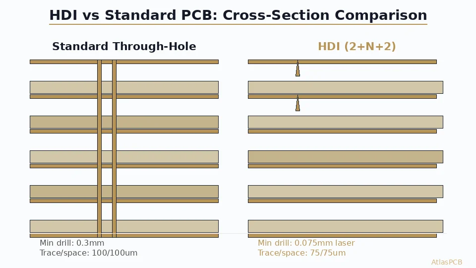
Constraint: Microvia aspect ratio must not exceed 1:1. A 100μm (4 mil) microvia in a 75μm (3 mil) dielectric has aspect ratio 0.75:1 — acceptable. The same via in a 120μm (4.7 mil) dielectric has aspect ratio 1.2:1 — marginal to unacceptable.
Impedance impact: Thinner buildup dielectrics require narrower traces to maintain 50Ω impedance. On a 60μm dielectric with Dk 4.0, a 50Ω microstrip trace is approximately 85μm (3.3 mil) wide — requiring fine-line capability from the manufacturer.
Step 5: Plan the Microvia Structure
Via-in-Pad
For fine-pitch BGAs, microvias are placed directly in the BGA pad (via-in-pad). This eliminates the need for a separate via pad and fan-out trace, saving space.
Requirements for via-in-pad:
- Via must be filled (copper or conductive paste)
- Surface must be planarized (≤15μm dimple per IPC-4761 Type VII)
- Specify in fab notes: “Via-in-pad, copper-filled and planarized”
Fan-Out Strategy
Dog-bone fan-out: Via is placed adjacent to the BGA pad, connected by a short trace. Used when via-in-pad is not needed or not available.
Direct via-in-pad: Microvia directly in the BGA pad. Saves space but requires filled vias.
For 1-N-1:
- Outer ring of BGA pads: route to edge without vias
- Inner ring: via-in-pad microvias L1→L2
- Core area: microvias L1→L2, then through-hole vias from L2 for deeper layer access
For 2-N-2:
- Outer ring: direct routing
- Second ring: L1→L2 microvias
- Inner rings: stacked microvias L1→L2→L3 for deep escape
Step 6: Validate with Manufacturer
This step is not optional. Send your preliminary stackup to the manufacturer before starting layout. The manufacturer validates:
- Material availability — Are the specified prepreg and core thicknesses available?
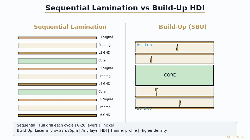
- Sub-lamination plan — Does the proposed layer structure match their sequential lamination process?
- Microvia feasibility — Can they drill the specified via size in the specified dielectric thickness?
- Impedance verification — Does the proposed geometry produce the target impedance with their actual Dk values?
- Total thickness — Is the final board thickness within spec for your application?
Common findings at validation:
- Specified dielectric is not available → manufacturer proposes nearest alternative
- Impedance requires trace width adjustment for actual Dk → manufacturer provides corrected values
- Via structure requires copper fill that was not specified → manufacturer adds requirement
- Total thickness exceeds target → need to reduce a dielectric or eliminate a layer
Getting this feedback before layout saves weeks compared to discovering it after Gerber submission.
Common HDI Stackup Mistakes
Mistake 1: Designing Without Manufacturer Input
The single most common and most expensive mistake. Your EDA tool does not know what prepreg thicknesses your manufacturer stocks, what microvia size they can drill, or how their sequential lamination process works.
Fix: Send stackup to manufacturer before layout. Get written confirmation of feasibility.
Mistake 2: Stacked Microvias Without Copper Fill
Stacked microvias with unfilled lower vias create a void that fails under thermal stress. This is a known reliability failure mode documented in IPC-2226.
Fix: Always specify copper-filled vias for any stacked microvia structure. Add to fab notes: “Stacked microvias must be copper-filled per IPC-4761 Type VII.”
Mistake 3: Exceeding Microvia Aspect Ratio
Laser-drilled microvias are reliable at aspect ratios ≤1:1. Exceeding this creates plating voids in the via barrel.
Fix: Ensure microvia diameter ≥ dielectric thickness. If you need a thicker dielectric, increase the via size proportionally.
Mistake 4: Impedance Not Calculated for Buildup Layers
Designers calculate impedance for core layers but forget that buildup layers have different (thinner) dielectrics. A 50Ω trace on a core layer is not 50Ω on a buildup layer if the dielectric thickness is different.
Fix: Calculate impedance separately for every unique dielectric-trace combination in the stackup.
Mistake 5: Asymmetric Buildup
A stackup with 2 buildup layers on top and 1 on bottom creates asymmetric stress that causes warpage.
Fix: Keep buildup symmetric: if you have 2 layers on top, have 2 on bottom. If your design only needs buildup on one side, add a dummy buildup on the other for mechanical balance.
How Atlas PCB Supports HDI Stackup Design
Atlas PCB provides engineering support for HDI stackup design — not just manufacturing. Our process:
- Review your BGA/routing requirements — determine minimum HDI order needed
- Propose stackup options — with actual materials from our stock
- Simulate impedance — on the proposed stackup using Polar SI field solver
- Validate with manufacturing — confirm sub-lamination plan, via feasibility, and total thickness
- Deliver verified stackup — ready for layout, with impedance-correct trace widths
This service is included with every HDI order — from 1-piece prototype to production. Send us your BGA datasheet and board requirements, and we will propose a stackup before you start layout.
Talk to an engineer about your HDI stackup requirements, or upload your Gerbers if you already have a design ready for review.
Frequently Asked Questions
How do I decide between 1-N-1, 2-N-2, and any-layer HDI?
The decision is primarily driven by BGA pitch. For 0.65-0.8mm pitch, 1-N-1 provides enough microvia density for fan-out with one level of laser vias. For 0.4-0.5mm pitch, 2-N-2 is typically required — two levels of microvias enable full BGA escape routing. Any-layer HDI is reserved for ≤0.4mm pitch or extremely area-constrained designs where every routing channel matters. Always start with the lowest HDI order that meets your requirements — each step up adds 30-50% in cost and manufacturing complexity.
What dielectric thickness should I use for HDI buildup layers?
Standard HDI buildup dielectrics range from 50-75μm (2-3 mil). This thickness supports 75-100μm laser-drilled microvias at acceptable aspect ratios (≤1:1). For high-density designs, 25-50μm (1-2 mil) dielectrics are used with smaller microvias. Choose your dielectric thickness based on three constraints: microvia aspect ratio (diameter ≥ dielectric thickness), impedance target (thinner dielectric needs narrower traces), and manufacturer’s available materials.
Do I need to coordinate my HDI stackup with the manufacturer?
Absolutely yes. HDI stackups must align with the manufacturer’s sequential lamination process, available prepreg/core thicknesses, laser drill capability, and via fill process. Designing without manufacturer input frequently results in stackups that cannot be built as specified — leading to costly redesign after Gerber submission. Best practice: send your preliminary stackup to the manufacturer before starting layout and get written confirmation of feasibility.
Related guides: [HDI PCB Manufacturer]/blog/hdi-pcb-manufacturer/) | [HDI PCB Technology]/blog/hdi-pcb-technology/) | [PCB Via Types Guide]/blog/pcb-via-types-guide/)
Further Reading
[HDI PCB Design Guide: Stackup Rules, Via Structures & DFM Checklist]/blog/hdi-pcb-design-guide/)
[PCB Sequential Lamination: Process, Design Rules, and When You Need It]/blog/pcb-sequential-lamination/)
[Via-in-Pad Design: Filled, Capped, and Plated Over — Complete Guide]/blog/via-in-pad-design/)
[Controlled Impedance PCB: Design, Stackup & Testing Explained]/blog/controlled-impedance-pcb/)
[High-Speed PCB Design: Signal Integrity Essentials for Modern Electronics]/blog/high-speed-pcb-design/)
[Multilayer PCB Stackup Design Guide: 8 to 30+ Layers Step by Step]/blog/multilayer-pcb-stackup-design-guide/)
[BGA Escape Routing: Strategies for 0.4mm, 0.5mm, and 0.8mm Pitch]/blog/bga-escape-routing/)
[PCB Pad Design for BGA, QFN, and Passive Components: Best Practices]/blog/pcb-pad-design-bga-qfn/)
[PCB Grounding Techniques: Star, Split, and Solid Ground Plane Strategies]/blog/pcb-grounding-techniques/)
About AtlasPCB — We specialize in complex PCB manufacturing for HDI, RF, and high-reliability applications. Explore our HDI PCB manufacturing capabilities, or get an multilayer PCB fabrication up to 30 layers . Every order includes free engineering review. Get your quote.
Reviewed by AtlasPCB Engineering Team — IPC-certified manufacturing specialists with 15+ years of production experience in HDI, RF, and high-reliability PCB fabrication. Content based on factory floor data and real customer design reviews.
- HDI stackup
- microvia
- pcb design
- sequential lamination
- high density interconnect