· AtlasPCB Engineering · Engineering · 4 min read
PCB Pad Design for BGA, QFN, and Passive Components: Best Practices
Optimize PCB pad design for reliable soldering — BGA pad strategies, QFN thermal pad design, passive component pad geometry for anti-tombstoning, and IPC-7351 land pattern standards.

Proper pad design is critical for reliable solder joints. Incorrect pad geometry leads to tombstoning, voiding, insufficient solder, or bridging. This guide covers pad design best practices for the most common component types.
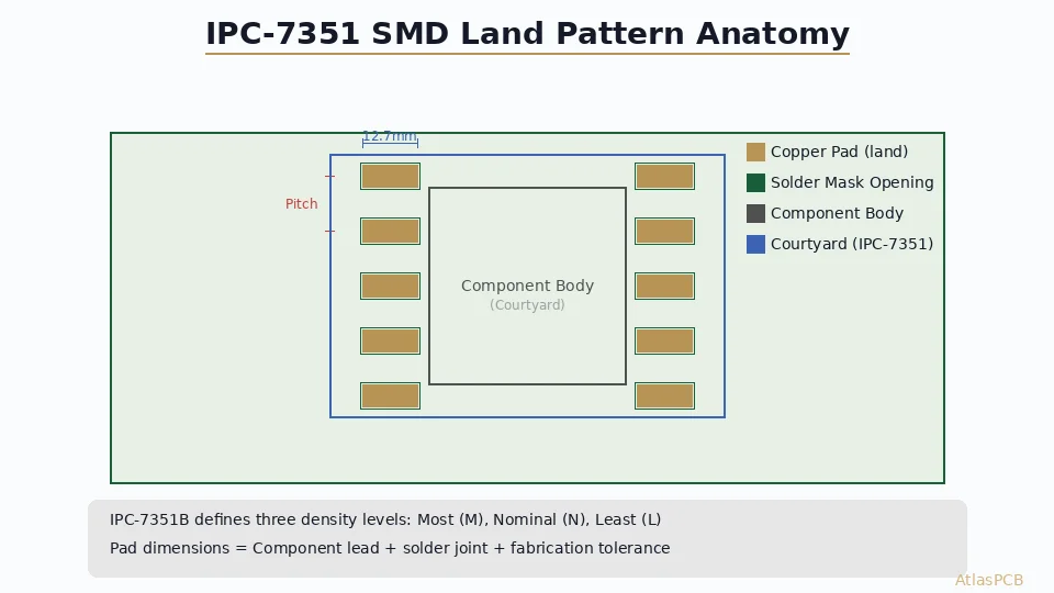
IPC-7351 Land Pattern Standard
IPC-7351 defines three density levels for pad design:
| Level | Description | Pad Size | Use Case |
|---|---|---|---|
| Level A (Most) | Maximum land size | Largest pads | Best soldering yield, prototyping |
| Level B (Nominal) | Standard land size | Medium pads | General production (recommended default) |
| Level C (Least) | Minimum land size | Smallest pads | Maximum density, experienced assembly |
BGA Pad Design
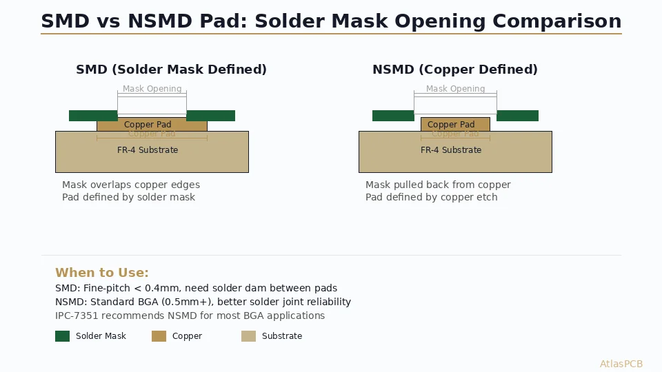
NSMD vs SMD Pads
NSMD (Non-Solder Mask Defined):
- Solder mask opening is larger than the copper pad
- Copper pad edges are exposed
- Preferred for >=0.65mm pitch: Provides more consistent pad size (defined by etching, not solder mask alignment)
- Solder joint is stronger (solder wraps around pad edge)
SMD (Solder Mask Defined):
- Solder mask opening is smaller than copper pad
- Solder mask constrains the solder to a smaller area
- Required for <=0.5mm pitch: NSMD pads are too small for reliable solder mask registration
BGA Pad Sizing
| BGA Pitch | Ball Diameter | NSMD Pad | SMD Opening | Solder Mask |
|---|---|---|---|---|
| 1.27mm | 0.76mm | 0.65mm | N/A | 0.75mm opening |
| 1.0mm | 0.60mm | 0.50mm | N/A | 0.60mm opening |
| 0.8mm | 0.45mm | 0.38mm | 0.35mm | 0.43mm opening |
| 0.65mm | 0.35mm | 0.30mm | 0.28mm | 0.35mm opening |
| 0.5mm | 0.30mm | 0.25mm | 0.23mm | 0.28mm opening |
| 0.4mm | 0.25mm | N/A | 0.20mm | 0.23mm opening |
Via-in-Pad for BGA
- Required for inner ball rows at <=0.65mm pitch
- Via must be filled (epoxy or copper) and cap-plated to create flat surface
- Without fill: solder wicks into via creating a void and weak joint
- With dogbone: route short trace (0.2mm wide) to adjacent via (0.8mm+ pitch)

QFN (Quad Flat No-Lead) Pad Design
QFN Ground/Thermal Pad
The exposed ground pad on the bottom of QFN packages requires special attention:
- Pad size: Match the component’s exposed pad specification (typically 80-90% of package dimension)
- Solder paste: Use a segmented stencil pattern (divided into 4-9 smaller squares) to reduce voiding. 50-60% paste coverage is typical.
- Thermal vias: Array of 0.3mm vias on 1.0mm pitch within the thermal pad. Use tented vias (solder mask covered) to prevent solder wicking.
- Solder mask: NSMD for signal pads; the thermal pad may be SMD or NSMD depending on manufacturer recommendation
QFN Signal Pad Design
- Pad extends 0.2-0.3mm beyond the QFN lead toe for visual inspection of solder fillet
- Pad width matches lead width (or slightly wider, +0.05mm per side)
- Solder mask opening: 0.05mm larger than copper pad per side
Passive Component Pad Design
Anti-Tombstoning Design
Tombstoning (one end lifts during reflow) is the #1 defect for small passives (0402, 0201).
Prevention through pad design:
- Symmetric pads: Both pads MUST be identical size and shape
- Equal copper connection: Same trace width entering both pads from same direction, or no trace (via only)
- Equal thermal mass: If one pad connects to a ground plane, use thermal relief on both pads (or neither)
- Pad extension: IPC-7351 Level B provides adequate anti-tombstone margin
Standard Passive Pad Sizes (Level B, Recommended)
| Package | Pad Width | Pad Length | Gap (center) |
|---|---|---|---|
| 0201 | 0.28mm | 0.30mm | 0.20mm |
| 0402 | 0.50mm | 0.50mm | 0.50mm |
| 0603 | 0.80mm | 0.80mm | 0.80mm |
| 0805 | 1.00mm | 1.20mm | 0.90mm |
| 1206 | 1.50mm | 1.50mm | 1.60mm |
Common Pad Design Mistakes
- Asymmetric passive pads — causes tombstoning
- BGA pad too small — insufficient solder volume, weak joints
- QFN thermal pad without segmented stencil — massive voiding (>50%)
- Missing thermal relief on plane-connected pads — cold joints during hand soldering
- Via-in-pad without fill — solder wicking creates voids
- Solder mask on pads — insufficient solder coverage area
Conclusion
Pad design directly impacts assembly yield and solder joint reliability. Follow IPC-7351 Level B as your default, use NSMD pads for BGA (>=0.65mm), segment the QFN thermal pad stencil, and ensure passive component pads are perfectly symmetric. These details may seem small, but they’re the difference between 99.9% yield and 95% yield at production volumes.
Further Reading
[Via-in-Pad Design: Filled, Capped, and Plated Over — Complete Guide]/blog/via-in-pad-design/)
[PCB Solder Mask: Types, Colors, and Functions Explained]/blog/pcb-solder-mask-guide/)
[BGA Soldering and Rework: Challenges, Inspection, and Best Practices]/blog/bga-soldering-rework/)
[PCB Grounding Techniques: Star, Split, and Solid Ground Plane Strategies]/blog/pcb-grounding-techniques/)
[HDI PCB Design Guide: Stackup Rules, Via Structures & DFM Checklist]/blog/hdi-pcb-design-guide/)
About AtlasPCB — We specialize in complex PCB manufacturing for HDI, RF, and high-reliability applications. Explore our HDI PCB manufacturing capabilities . Every order includes free engineering review. Get your quote.
Reviewed by AtlasPCB Engineering Team — IPC-certified manufacturing specialists with 15+ years of production experience in HDI, RF, and high-reliability PCB fabrication. Content based on factory floor data and real customer design reviews.
- pad design
- BGA
- QFN
- land pattern