· AtlasPCB Engineering · Engineering · 5 min read
PCB Grounding Techniques: Star, Split, and Solid Ground Plane Strategies
Master PCB grounding — understand solid ground planes, star grounding, split planes, analog-digital ground separation, and best practices for noise-free circuit operation.

Proper grounding is the foundation of every well-functioning electronic circuit. Poor grounding causes noise coupling, ground bounce, EMI failures, and mysterious intermittent issues. This guide explains the most effective PCB grounding strategies.
Why Grounding Matters
The ground system serves three critical functions:
- Signal return path: Every signal current must return to its source through the ground
- Reference voltage: Ground defines the 0V reference for all circuits
- Shielding: Ground planes shield sensitive circuits from external interference
When ground is compromised, signals have no clean return path, reference voltages shift, and circuits malfunction.
Grounding Strategies
1. Solid Ground Plane (Recommended Default)
A continuous, unbroken copper ground plane on one or more layers.
Advantages:
- Lowest impedance return path for all signals
- Best EMI shielding
- Consistent impedance for controlled impedance traces
- Simplifies design — one ground for everything
When to use: Almost always. This is the default recommendation for 90% of PCB designs.
Key rules:
- No slots, cuts, or splits under high-speed signal traces
- No routing of signal traces on ground plane layers
- Via stitching around the board perimeter (every 5-10mm)
2. Star Grounding
All ground connections radiate from a single common point, like a star. Used primarily in audio and precision analog circuits.
Advantages:
- Prevents ground current from one circuit flowing through another circuit’s ground path
- Excellent for low-frequency analog (audio, precision measurement)
Disadvantages:
- Only works at low frequencies (below ~1 MHz)
- Impractical for high-density digital boards
- Long ground traces have high inductance
When to use: Audio amplifiers, precision DAC/ADC reference circuits, laboratory instrumentation.
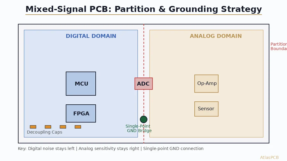
3. Split Ground Plane
The ground plane is physically divided into separate regions (analog ground, digital ground, power ground) connected at a single point.
Advantages:
- Prevents digital switching noise from coupling into sensitive analog circuits
- Each ground domain has clean return paths within its region
Disadvantages:
- Signals crossing the split create large return current loops (EMI nightmare)
- Must carefully route all signals to stay within their ground domain
- Complexity increases dramatically with multiple splits
When to use: Mixed-signal boards with high-resolution ADCs (>16-bit) where analog noise floor is critical. But even then, a solid plane with careful partitioning is often better.

Analog-Digital Ground Separation
The most common grounding question: “Should I separate analog and digital ground?”
Modern Best Practice: Single Ground Plane with Partitioning
- Use a single, solid ground plane — no splits
- Partition the layout: Place analog components in one area, digital in another
- Route signals carefully: Keep digital noise current away from analog signal paths
- Connect ADC/DAC AGND and DGND pins together at the IC (follow datasheet recommendation)
- Use guard traces or ground copper between sensitive analog and noisy digital traces
Why Single Ground Is Usually Better
- Split planes create return current discontinuities that are worse than the noise they prevent
- Modern ADCs and mixed-signal ICs are designed for single ground plane operation
- The IC’s internal AGND/DGND connection is already optimized
When Split Ground Is Still Appropriate
- Isolated power supplies (galvanic isolation)
- Safety isolation requirements (medical, high voltage)
- Very high-precision measurement (24-bit ADC with nanovolt sensitivity)
Ground Bounce
What It Is
When multiple digital outputs switch simultaneously, the transient current through ground inductance creates a voltage spike on the ground rail. This shifts the ground reference voltage temporarily, potentially causing logic errors.
How to Minimize
- Multiple ground vias near IC ground pins (reduces inductance)
- Decoupling capacitors close to power/ground pins
- Controlled slew rate outputs where possible
- Spread switching events — avoid simultaneous output transitions
- Low-ESL capacitors (reverse geometry, LICC) for high-speed decoupling
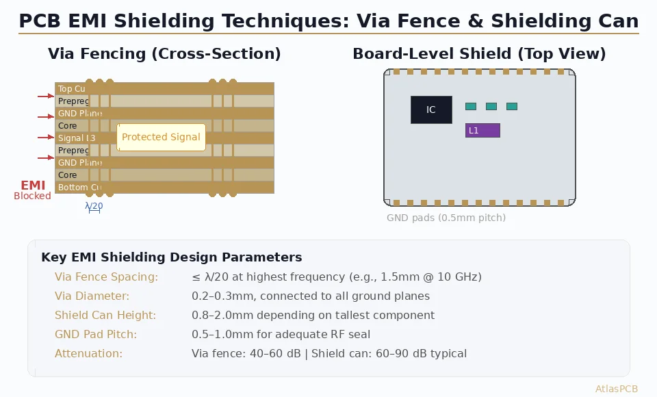
Via Stitching
Ground via stitching connects ground planes on different layers and provides shielding.
Guidelines
- Board perimeter: Via stitching every 5-10mm around the board edge creates a ground cage
- Between sections: Via fence between RF and digital sections
- Under ground pours: Every 5-10mm to ensure the pour is actually connected to the ground plane
- Near signal vias: Place a ground via within 1mm of every high-speed signal via (provides local return path)
- Via diameter: 0.3mm typical, same as standard vias
Common Grounding Mistakes
- Routing traces across ground plane splits — creates huge EMI loop
- Connecting ground only at board edge — long ground path = high inductance
- Ground pour islands — floating copper not connected to ground is worse than no copper
- Daisy-chaining ground through multiple components — creates shared impedance
- Ignoring return current path — every signal needs a low-impedance return, and it flows on the nearest reference plane directly under the signal trace
Conclusion
Start with a solid ground plane — it’s correct for the vast majority of designs. Only consider split grounds for specific isolation requirements. Partition your layout to separate noisy and sensitive circuits physically, not electrically. Follow the IC manufacturer’s grounding recommendations, use adequate decoupling, and stitch your ground planes with vias. Good grounding is invisible when done right but painfully obvious when done wrong.
Further Reading
[Controlled Impedance PCB: Design, Stackup & Testing Explained]/blog/controlled-impedance-pcb/)
[EMC/EMI Design for PCBs: Passing Compliance on the First Try]/blog/emc-emi-pcb-design/)
[IPC Class 3 Requirements: The Complete Guide for Designers]/blog/ipc-class-3-requirements/)
About AtlasPCB — We specialize in complex PCB manufacturing for HDI, RF, and high-reliability applications. Explore our impedance-controlled PCB manufacturing . Every order includes free engineering review. Get your quote.
Reviewed by AtlasPCB Engineering Team — IPC-certified manufacturing specialists with 15+ years of production experience in HDI, RF, and high-reliability PCB fabrication. Content based on factory floor data and real customer design reviews.
- grounding
- EMI
- pcb design
- noise reduction