· AtlasPCB Engineering · Engineering · 7 min read
PCB Sequential Lamination: Process, Design Rules, and When You Need It
A practical guide to PCB sequential lamination — what it is, how it works, when your board requires it, and the design rules that prevent costly manufacturing failures. Covers sub-composite planning, registration tolerance, material selection, and cost optimization.
Sequential lamination is the manufacturing process that makes complex multilayer PCBs possible. If your board uses blind vias, buried vias, or any HDI microvia structure, it goes through sequential lamination — and your design decisions directly affect whether it gets built reliably or becomes an expensive pile of scrap.
This guide covers the process, the design rules you need to follow, and the cost tradeoffs that matter when specifying a sequentially laminated board.
What Is Sequential Lamination?
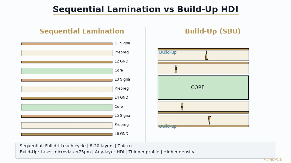
Standard PCB lamination bonds all layers at once in a single press cycle. You stack prepreg, copper foil, and inner layer cores, apply heat and pressure, drill all the way through, and plate. Every via spans the full stackup.
Sequential lamination builds the board in stages. The manufacturer starts with one or more inner cores, drills and plates vias on those cores (creating buried vias), then bonds additional layers on top through another full press cycle. This process repeats until all layers are complete.
Single Lamination vs Sequential Lamination
Single Lamination
Sequential Lamination
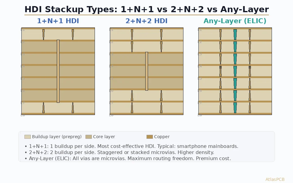
Each cycle is called a lamination stage or sub-composite. A typical 12-layer board with blind and buried vias might require 2-3 lamination stages, while a complex HDI board with 5+N+5 structure requires 10+ stages.
Why It Matters
Without sequential lamination, every via must pass through every layer. That wastes routing real estate on inner layers and limits design density. Sequential lamination enables:
- Buried vias — connect inner layers without touching the surface
- Blind vias — connect a surface layer to inner layers without penetrating the full board
- Stacked and staggered microvias — HDI structures with laser-drilled vias built up one layer at a time
- Higher routing density — inner layers freed from through-via obstacles
The Sequential Lamination Process
Stage 1: Core Fabrication
The process begins with inner layer cores — double-sided copper-clad laminate with circuits etched on both sides.
- Inner layers are imaged, etched, and inspected (AOI)
- Critical cores receive buried vias: drilled, plated, and filled
- Each core is a self-contained unit with its own registration targets
Stage 2: First Lamination
The inner cores are stacked with prepreg (uncured fiberglass/resin sheets) and additional copper foil. This assembly goes into a hydraulic press:
- Temperature: 180–200°C (typical for FR-4/high-Tg materials)
- Pressure: 200–400 PSI
- Duration: 60–120 minutes depending on stackup thickness
After pressing, the assembly is a solid panel. New drill holes (blind vias) are drilled from the outside surface into — but not through — the panel.
Stage 3: Drill and Plate
Blind vias are drilled (mechanical or laser), then plated with copper. For HDI, laser drilling creates microvias (typically 75–150μm diameter) that are then copper-filled.
Stage 4: Repeat
Additional layers are added through further lamination cycles. Each cycle repeats: layup → press → drill → plate.
Final Stage: Through-Hole Vias and Surface Finish
After all sequential laminations are complete, through-hole vias (spanning the full stackup) are drilled, plated, and the board receives its surface finish (ENIG, HASL, etc.).

Design Rules for Sequential Lamination
1. Plan Your Sub-Composites First
Before drawing a single trace, define your lamination stages. Each stage must be a viable standalone unit that can be processed independently.
| Stackup Type | Lamination Stages | Build Sequence |
|---|---|---|
| 8L with blind vias | 2 | Core (L3–L6) → add L1-2 & L7-8 |
| 12L blind + buried | 3 | Core (L5–L8) → blind vias → add L1-4 & L9-12 |
| 1+N+1 HDI | 2 | Core (standard ML) → HDI buildup layers |
| 2+N+2 HDI | 4 | Core → HDI L1 → HDI L2 (both sides) |
| 3+N+3 HDI | 6 | Core → 3 sequential HDI buildups per side |
Rule: The stackup must be symmetric about the center. Asymmetric stackups warp during lamination because the resin flow and thermal expansion are uneven.
2. Registration Tolerance Budget
Each lamination cycle introduces registration error. These errors are cumulative.
| Parameter | IPC Class 2 | IPC Class 3 |
|---|---|---|
| Layer-to-layer registration | ±100μm (4 mil) | ±75μm (3 mil) |
| Layer-to-drill registration | ±125μm (5 mil) | ±100μm (4 mil) |
| Cumulative (3 stages) | ±175μm (7 mil) | ±130μm (5 mil) |
Design impact: Your annular ring must accommodate the worst-case cumulative registration error. For each additional lamination stage, add 25–50μm (1–2 mil) to your annular ring calculation. If your CAD tool’s default annular ring works for single lamination, it probably does not work for sequential.
3. Material Selection
The dielectric material must survive multiple thermal cycles without degradation.
| Property | Single Lam. | 2–3 Cycles | 4+ Cycles |
|---|---|---|---|
| Minimum Tg | 130°C | 170°C | 170–180°C |
| Minimum Td | 300°C | 340°C | 350°C+ |
| Z-axis CTE | <70 ppm/°C | <60 ppm/°C | <50 ppm/°C |
| Recommended | S1000-2, IT158 | S1170G, IT180A | Megtron 6, TU-872 |
Why this matters: Each press cycle subjects the entire assembly to 180–200°C. Standard FR4 (Tg 130°C) softens above its Tg, causing layer shift, delamination, and barrel crack in plated vias. High-Tg materials maintain dimensional stability through repeated thermal excursions.
4. Via Fill Requirements
In sequential lamination, any via that will have additional layers built on top of it must be filled and planarized.
- Unfilled vias under new lamination create resin voids (outgassing) and dimples that compromise the next layer’s adhesion
- Copper fill (electroplated) is the standard for HDI microvias — provides the best thermal and electrical reliability
- Resin fill + cap plate is acceptable for larger mechanical vias (>0.3mm) that serve as buried vias
5. Keep Copper Balance Symmetric
Each sub-composite should have approximately equal copper distribution on both sides. Copper imbalance causes:
- Differential thermal expansion during pressing
- Panel bow and twist after lamination
- Registration shift in subsequent stages
Rule of thumb: Keep copper coverage within 15% between paired layers (e.g., L1 vs L2, L3 vs L4).
Cost Optimization Strategies
Sequential lamination is inherently expensive. Here is how to minimize cost without compromising design intent.
Cost Impact by Lamination Stages
Relative cost multiplier vs single-lamination board of equivalent layer count
Reduce Lamination Stages
Every eliminated stage saves 30–50% of incremental cost. Common optimizations:
- Use through-hole vias where possible — if a connection spans the full stack, a through-hole via costs nothing extra
- Consolidate blind vias — if blind vias on layer 1→2 and layer 1→3 can be replaced with a single 1→3 blind via, you eliminate one drill operation
- Consider staggered vs. stacked microvias — staggered microvias avoid the need for copper fill between stages
Right-Size Your Stackup
Not every 12-layer board needs sequential lamination. Ask:
- Can through-hole vias route the same connections? (Often yes, with creative routing)
- Can you eliminate 2 layers by using blind vias, but the blind vias require sequential lamination — is the net cost lower? (Run the numbers with your manufacturer)
- Is the density truly needed, or can a larger board area avoid HDI entirely?
Communicate Early with Your Manufacturer
Your PCB manufacturer’s CAM team can review your proposed stackup before you finalize the design. A good manufacturer will:
- Confirm the stackup is manufacturable at their facility
- Identify cost-saving alternatives (e.g., different via structures)
- Flag registration risks before they become production failures
At AtlasPCB, every sequentially laminated order goes through a 12-hour human engineering review specifically because these boards have the highest DFM failure rate. We catch stackup problems before they reach production.
Key Takeaways
Sequential lamination enables blind vias, buried vias, and HDI — if your design uses any of these, it requires sequential lamination
Design the stackup first, route second — sub-composite planning determines everything else
Registration tolerances are cumulative — add annular ring margin for each lamination stage
Use high-Tg materials — standard FR4 will not survive multiple press cycles reliably
Fill all vias that will be laminated over — unfilled vias cause voids and delamination
Optimize for fewer stages — every eliminated lamination cycle saves 30-50% incremental cost
Need help with a sequentially laminated PCB? Upload your Gerber files for a free engineering review, or talk to an engineer about your stackup requirements.
Further Reading
[HDI PCB Design Guide: Stackup Rules, Via Structures & DFM Checklist]/blog/hdi-pcb-design-guide/)
[HDI PCB Technology: Microvias, Laser Drilling, and High-Density Design]/blog/hdi-pcb-technology/)
[Blind Via vs Buried Via: Design Rules, Cost Impact & When to Use Each]/blog/blind-via-vs-buried-via/)
[High-Multilayer FR4 vs Standard FR4: When to Upgrade Material Grade]/blog/high-multilayer-fr4-vs-standard-fr4/)
[PCB DFM Checklist: 50 Points to Review Before Sending Gerbers]/blog/pcb-dfm-checklist/)
[PCB Manufacturer with Engineering Review: Why Human DFM Audit Matters]/blog/pcb-manufacturer-engineering-review/)
[PCB Manufacturing Process: 15 Steps from Gerber to Finished Board]/blog/pcb-manufacturing-process-15-steps/)
[PCB Gerber Files: What They Are and How to Generate Them]/blog/pcb-gerber-files-guide/)
[ENEPIG vs ENIG: Which PCB Surface Finish for Your Design?]/blog/enepig-vs-enig/)
[PCB Surface Finish Guide: HASL, ENIG, OSP and More Compared]/blog/pcb-surface-finish-guide/)
About AtlasPCB — We specialize in complex PCB manufacturing for HDI, RF, and high-reliability applications. Explore our HDI PCB manufacturing capabilities, multilayer PCB fabrication up to 30 layers, or get an full PCB manufacturing capabilities . Every order includes free engineering review. Get your quote.
Reviewed by AtlasPCB Engineering Team — IPC-certified manufacturing specialists with 15+ years of production experience in HDI, RF, and high-reliability PCB fabrication. Content based on factory floor data and real customer design reviews.
- sequential lamination
- multilayer pcb
- pcb manufacturing
- HDI
- pcb stackup
- high layer count