· AtlasPCB Engineering · Engineering · 12 min read
PCB Manufacturing Process: 15 Steps from Gerber to Finished Board
A complete walkthrough of the PCB manufacturing process in 15 steps — from Gerber file input through inner layer imaging, lamination, drilling, plating, solder mask, surface finish, to electrical testing and final inspection.
Understanding how PCBs are manufactured helps you design better boards, communicate more effectively with your manufacturer, and diagnose problems when they occur. This guide walks through the complete manufacturing process in 15 steps, with emphasis on what matters for quality and what can go wrong.
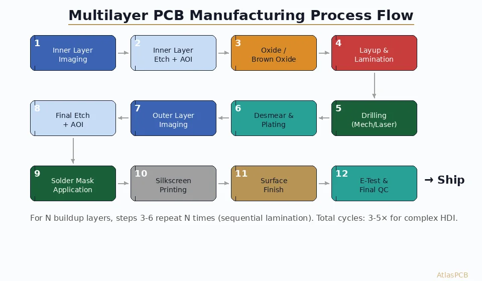
Overview: The 15 Steps
| Step | Process | Critical For |
|---|---|---|
| 1 | Engineering review / CAM | Catching design issues before production |
| 2 | Inner layer imaging | Trace accuracy on inner layers |
| 3 | Inner layer etching | Trace width control |
| 4 | AOI (inner layer) | Defect detection before lamination |
| 5 | Oxide treatment | Layer adhesion during lamination |
| 6 | Layup and lamination | Dielectric thickness, impedance, registration |
| 7 | Drilling | Hole position, size, quality |
| 8 | Desmear + electroless copper | Via connectivity |
| 9 | Electrolytic copper plating | Via reliability, conductor thickness |
| 10 | Outer layer imaging | Outer trace accuracy |
| 11 | Outer layer etching | Outer trace width control |
| 12 | Solder mask | Insulation, solder control |
| 13 | Surface finish | Solderability, shelf life |
| 14 | Routing / profiling | Board dimensions |
| 15 | Electrical test + final inspection | Functionality verification |
Step 1: Engineering Review and CAM Processing
Before any physical manufacturing begins, the manufacturer’s CAM (Computer-Aided Manufacturing) team processes your design files.
What happens:
- Gerber files are imported and verified for completeness
- Layer registration is checked (copper to drill alignment)
- Design rules are verified against manufacturing capability
- Panelization — your board is arranged in an array on a production panel (typically 18” × 24” or 21” × 24”)
- Impedance is simulated on the actual stackup
- Tooling holes, fiducials, and test coupons are added to the panel
What can go wrong: Missing layers, mismatched drill-to-copper alignment, impedance incompatibility with available materials. This is why human engineering review matters — see our [engineering review guide]/blog/pcb-manufacturer-engineering-review/) for detail on what a proper review catches.
Step 2: Inner Layer Imaging
For multilayer boards (4+ layers), inner layer copper patterns are created through photolithographic imaging.
Process:
- Clean copper-clad laminate (core material) is coated with photosensitive dry film resist
- A phototool (or LDI — Laser Direct Imaging) exposes the resist with the circuit pattern
- Unexposed resist is developed (washed away), leaving resist covering the areas that should remain as copper
Key quality factors:
- LDI vs phototool: LDI (Laser Direct Imaging) provides ±0.5 mil accuracy with no phototool distortion. Film-based phototools are cheaper but introduce dimensional error from film stretch and alignment.
- Clean room environment: Particles trapped under the resist cause open circuits or short circuits. Inner layer imaging should happen in a controlled environment (Class 10,000 or better).
- Registration accuracy: The pattern must align precisely to tooling holes that will be used for layer-to-layer registration during lamination.
Step 3: Inner Layer Etching
The exposed copper (areas not protected by resist) is chemically removed, leaving the circuit pattern.
Process:
- The panel passes through an etching machine (typically cupric chloride or ammoniacal etchant)
- Etchant dissolves exposed copper
- Remaining resist is stripped, revealing the finished copper pattern
Critical parameter — etch factor: Etching is not perfectly vertical. The etchant undercuts beneath the resist, creating a trapezoidal trace cross-section instead of rectangular. The ratio of copper thickness to undercut is the etch factor (typically 3:1 for standard processes).
Impact on impedance: The trapezoidal cross-section affects impedance. A 5 mil designed trace may etch to 4.2 mil at the top and 5 mil at the base. Field solvers account for this — simple impedance calculators do not.
Impact on fine lines: For trace widths below 3 mil, etch factor becomes the limiting factor. This is why ultra-fine-line circuits require special processes (semi-additive or modified semi-additive).
Step 4: Automated Optical Inspection (AOI)
After etching, every inner layer is inspected by AOI — a camera-based system that compares the actual copper pattern to the design data.
What AOI catches:
- Open circuits (broken traces)
- Short circuits (copper bridges between traces)
- Trace width violations
- Missing features
- Registration errors
Why this matters: Inner layer defects discovered after lamination are irreparable — the board is scrap. AOI at this stage catches defects before the expensive lamination step, saving material and time.
Limitation: AOI catches pattern defects visible from above. It does not detect subsurface issues (voids in copper, laminate defects) that require cross-section or electrical testing.
Step 5: Oxide Treatment (Brown Oxide / Black Oxide)
Before lamination, inner layer copper surfaces are chemically treated to improve adhesion to the prepreg resin.
Process: The copper surface is treated with a chemical oxide process (brown oxide or black oxide) that creates a micro-rough copper oxide layer. This increases the copper surface area and creates a mechanical bond with the prepreg resin during lamination.
Alternative: Some manufacturers use organic bonding agents (reduced oxide alternatives) that provide adhesion without the oxide layer. These are common for fine-line inner layers where oxide crystals could bridge narrow gaps.
What can go wrong: Insufficient oxide treatment leads to delamination — layers separating under thermal stress. Excessive treatment can cause oxide crystals to bridge between closely spaced traces, creating shorts (known as “pink ring” defects).
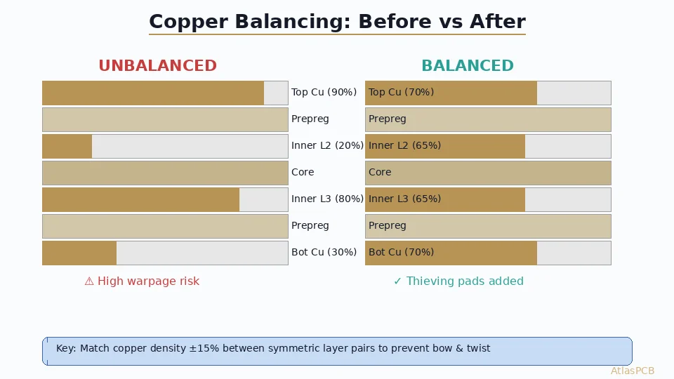
Step 6: Layup and Lamination
This is the most critical step for multilayer boards. All layers are assembled and permanently bonded under heat and pressure.
Process:
- Layup: Inner layers, prepreg sheets, and outer copper foils are stacked in precise order using registration pins or optical alignment
- Press loading: The stack is placed in a hydraulic press (vacuum-assisted for high-layer-count boards)
- Heating: Temperature ramps to 180-190°C (for standard FR4), melting the prepreg resin
- Pressure: 250-400 PSI forces resin to flow and fill the spaces around inner layer copper patterns
- Cure: Temperature is held for 60-120 minutes to fully cure the resin
- Cool-down: Controlled cooling to prevent thermal shock and warpage
Critical parameters:
- Temperature profile: Too hot = resin degradation, excessive flow. Too cool = incomplete cure, delamination risk.
- Pressure: Too high = crushed dielectric (impedance shift), too low = voids and poor adhesion.
- Vacuum: Essential for removing air bubbles that become delamination initiation sites.
- Registration: Layer-to-layer alignment must be maintained through the entire press cycle. For high-layer-count boards, this is the primary quality challenge.
For sequential lamination (HDI, 10+ layer boards with buried vias): Steps 2-6 are repeated for each sub-lamination, with the previously laminated structure used as a “core” for the next buildup.
Step 7: Drilling
After lamination, holes are drilled through the panel for vias and component mounting.
Process types:
| Drill Type | Method | Min Diameter | Application |
|---|---|---|---|
| Through-hole | Mechanical CNC | 0.15mm (6 mil) | Standard vias, component holes |
| Blind via | Controlled depth CNC | 0.15mm (6 mil) | L1 to L2/L3 connections |
| Blind microvia | UV/CO2 laser | 0.075mm (3 mil) | HDI L1-L2 connections |
| Buried via | Mechanical (in sub-lam) | 0.15mm (6 mil) | Inner layer connections |
| Back-drill | Controlled depth CNC | 0.45mm (18 mil) | Stub removal for high-speed |
Critical parameters:
- Position accuracy: ±1-2 mil for standard, ±0.5 mil for HDI. Determines annular ring compliance.
- Hole quality: Clean hole walls are essential for plating adhesion. Smear (resin residue) on hole walls blocks copper deposition.
- Aspect ratio: Board thickness ÷ drill diameter. Most manufacturers reliable up to 10:1; above that requires specialized process.
- Drill wear: Drill bits degrade with use. A worn bit produces oversized, rough holes. Hit counts (holes per bit) are controlled — typically 500-3000 hits depending on material and drill size.
Step 8: Desmear and Electroless Copper
After drilling, holes are chemically processed to prepare for plating.
Desmear: Chemical (potassium permanganate) or plasma treatment removes resin smear from hole walls. Smear blocks copper-to-copper connections at inner layer intersections. This step is critical — insufficient desmear causes intermittent connections.
Electroless copper: A thin layer of copper (0.5-1.0μm) is deposited on hole walls through chemical reduction. This makes the non-conductive hole wall electrically conductive so that electrolytic plating can follow.
For PTFE materials: Chemical desmear does not work. Plasma desmear is required — a separate piece of equipment that not all manufacturers have.
Step 9: Electrolytic Copper Plating
Copper is electroplated onto the panel surface and into the holes to build up conductor thickness.
Targets:
- Hole barrel plating: ≥20μm (Class 2), ≥25μm (Class 3)
- Surface copper: ≥25μm total (base copper + plated copper)
Process challenges:
- Throwing power: Getting plating deep into high-aspect-ratio holes. The center of a deep hole plates slower than the opening, creating a “dogbone” profile. Modern pulse plating and additive chemistry improve throwing power.
- Uniformity: Copper thickness varies across the panel — edges plate thicker than the center. Anode geometry, bath agitation, and current density control manage this variation.
- Via fill: For copper-filled vias (required for HDI stacked microvias and via-in-pad), specialized DC plating with bottom-up fill chemistry is used.
Step 10: Outer Layer Imaging
The outer copper pattern is created using the same photolithographic process as inner layers (Step 2), but applied to the outer surfaces of the laminated panel.
Two main approaches:
- Tent and etch: Resist covers the traces; exposed copper is etched away (similar to inner layers)
- Pattern plating: Resist covers the spaces; copper + tin/tin-lead is plated onto exposed traces; resist is stripped; the thin copper between traces is etched away while the plated tin protects the traces
Pattern plating is more common for fine-line outer layers because it achieves better trace definition.
Step 11: Outer Layer Etching
Excess copper is removed from outer layers, completing the circuit pattern.
Process is similar to Step 3, with an additional consideration: the tin or tin-lead plating from pattern plating must be stripped after etching.
Outer layer etch factor is typically worse than inner layers because the copper is thicker (base copper + plated copper). This is why outer layer minimum trace width is often larger than inner layer minimum.
Step 12: Solder Mask Application
Solder mask (typically green, though other colors are available) is applied to protect copper from oxidation, prevent solder bridging during assembly, and provide electrical insulation.
Process:
- Liquid photoimageable (LPI) solder mask is applied by screen printing or curtain coating
- The mask is exposed through a phototool with the solder mask pattern (openings over pads)
- Unexposed mask is developed (washed away), opening the pads
- The mask is thermally cured
Key quality factors:
- Registration: Solder mask must align to the copper pattern within the specified tolerance (typically ±2-3 mil)
- Thickness: 0.5-1.5 mil over traces. Too thin = poor insulation. Too thick = interference with fine-pitch pads.
- Dam width: Minimum solder mask dam between adjacent pads. Typically 3-4 mil minimum. Below this, the dam breaks during development.
- Impedance impact: Solder mask adds 1-3Ω to surface microstrip impedance. This should be included in impedance modeling.
Step 13: Surface Finish
The exposed copper pads receive a surface finish to protect against oxidation and provide a solderable surface.
| Finish | Process | Shelf Life | Planarity | Cost | Best For |
|---|---|---|---|---|---|
| HASL (leaded) | Hot air solder leveling | 12+ months | Poor | Low | General through-hole |
| Lead-free HASL | Same, lead-free solder | 12+ months | Poor | Low-Med | RoHS, through-hole |
| ENIG | Electroless Ni + immersion Au | 12+ months | Excellent | Medium | BGA, fine-pitch |
| OSP | Organic solderability preservative | 6 months | Excellent | Low | Cost-sensitive SMT |
| Immersion silver | Chemical silver deposition | 6 months | Excellent | Medium | High-frequency |
| Immersion tin | Chemical tin deposition | 6 months | Good | Medium | Press-fit |
| ENEPIG | Ni + Pd + Au | 12+ months | Excellent | High | Wire bonding, mixed assembly |
For controlled impedance: HASL creates uneven pad surfaces (dome shape) that can affect impedance on surface traces near pads. ENIG, OSP, and immersion finishes provide flat surfaces.
For high-frequency: Immersion silver has the lowest impact on RF signal loss among common finishes. ENIG’s nickel layer is magnetic and lossy at RF frequencies.
Step 14: Routing and Profiling
Individual boards or arrays are cut from the production panel.
Methods:
- CNC routing: Standard method, ±2 mil accuracy, smooth edges
- V-scoring: Shallow grooves cut on both sides for snap-apart arrays
- Tab routing: Boards connected by breakaway tabs in panelized arrays
- Laser routing: For very tight tolerances or thin boards
Controlled-depth routing is used for features like edge plating cavities and stepped boards.
Step 15: Electrical Testing and Final Inspection
Electrical test: Every board undergoes 100% continuity and isolation testing.
- Flying probe: Two or more probes test each net for continuity and each gap for isolation. Slower but requires no custom fixture. Standard for prototypes.
- Bed of nails (fixture test): All points tested simultaneously using a custom fixture. Fast but requires fixture investment. Standard for production quantities.
Final inspection:
- Visual inspection under magnification (IPC-A-600 criteria)
- Dimensional measurement
- Impedance test data review (if applicable)
- Documentation compilation (CoC, test data, material certs for Class 3)
- Packaging for shipment
How Atlas PCB Ensures Quality Across All 15 Steps
Atlas PCB’s manufacturing partners maintain process controls at every step:
- Step 1: 12-hour human engineering review on every order
- Steps 2-3: LDI for inner layer imaging (no film distortion)
- Step 4: 100% AOI on inner layers before lamination
- Step 6: Vacuum-assisted press with programmable profiles per material
- Step 7: CNC drill with automatic tool measurement + laser drill for HDI
- Step 9: Pulse plating with throwing power control for high-aspect-ratio vias
- Step 12: LPI solder mask with ±2 mil registration
- Step 15: 100% electrical test + TDR impedance verification for controlled impedance orders
Every shipment includes quality documentation appropriate to the product class.
Frequently Asked Questions
How long does PCB manufacturing take?
Prototype lead times: 2-4 layer boards take 5-7 working days, 6-8 layers take 7-10 days, 10-16 layers take 10-15 days, and 20+ layers take 15-25 days with standard materials in stock. HDI, blind/buried vias, special materials, and IPC Class 3 testing add 3-10 days. These timelines start after engineering review is complete and files are approved for production.
What files does a PCB manufacturer need?
A complete fabrication package includes: Gerber files (RS-274X or Gerber X2) for every copper, mask, and silkscreen layer plus board outline; Excellon drill files for each drill type; a fabrication drawing with stackup, impedance, material, and finish specifications; and any special instructions. Missing or ambiguous files delay production. The most common issue is incomplete drill information for boards with multiple drill types (through, blind, buried).
What is the most critical step in PCB manufacturing?
For multilayer boards, lamination (Step 6) is most critical because it permanently bonds layers, determines dielectric thickness, and sets impedance. Lamination errors are irreversible. For all boards, drilling (Step 7) and plating (Step 9) are critical for via reliability — the plated through-hole is the most mechanically stressed feature during thermal cycling.
Summary
- PCB manufacturing involves 15 major steps from Gerber input to finished board
- Lamination is the most critical step for multilayer boards — it sets dielectric thickness and impedance
- Inner layer AOI before lamination catches defects that would otherwise scrap the entire panel
- Drill quality and plating thickness determine via reliability
- Surface finish choice affects solderability, shelf life, impedance, and cost
- 100% electrical testing verifies connectivity on every board
Ready to manufacture your next board? Upload your Gerbers for a free engineering review — we catch issues at Step 1 so they do not become problems at Step 15.
Related guides: [PCB Manufacturer with Engineering Review]/blog/pcb-manufacturer-engineering-review/) | [PCB DFM Checklist]/blog/pcb-dfm-checklist/) | [PCB Testing Methods]/blog/pcb-testing-methods/)
Further Reading
[HDI PCB Design Guide: Stackup Rules, Via Structures & DFM Checklist]/blog/hdi-pcb-design-guide/)
[HDI PCB Technology: Microvias, Laser Drilling, and High-Density Design]/blog/hdi-pcb-technology/)
[PCB Sequential Lamination: Process, Design Rules, and When You Need It]/blog/pcb-sequential-lamination/)
[Via-in-Pad Design: Filled, Capped, and Plated Over — Complete Guide]/blog/via-in-pad-design/)
[Blind Via vs Buried Via: Design Rules, Cost Impact & When to Use Each]/blog/blind-via-vs-buried-via/)
[Controlled Impedance PCB: Design, Stackup & Testing Explained]/blog/controlled-impedance-pcb/)
[PCB Gerber Files: What They Are and How to Generate Them]/blog/pcb-gerber-files-guide/)
[ENEPIG vs ENIG: Which PCB Surface Finish for Your Design?]/blog/enepig-vs-enig/)
[PCB Surface Finish Guide: HASL, ENIG, OSP and More Compared]/blog/pcb-surface-finish-guide/)
[PCB Solder Mask: Types, Colors, and Functions Explained]/blog/pcb-solder-mask-guide/)
About AtlasPCB — We specialize in complex PCB manufacturing for HDI, RF, and high-reliability applications. Explore our full PCB manufacturing capabilities . Every order includes free engineering review. Get your quote.
Reviewed by AtlasPCB Engineering Team — IPC-certified manufacturing specialists with 15+ years of production experience in HDI, RF, and high-reliability PCB fabrication. Content based on factory floor data and real customer design reviews.
- pcb manufacturing
- fabrication process
- inner layer
- lamination
- plating
- solder mask