· AtlasPCB Engineering · Engineering · 7 min read
ENEPIG vs ENIG: Which PCB Surface Finish for Your Design?
Detailed comparison of ENEPIG and ENIG surface finishes for PCB manufacturing. Covers layer structure, cost, wire bonding capability, signal integrity, and decision criteria for RF, BGA, and mixed-technology boards.
Surface finish selection determines solder joint reliability, wire bonding capability, and long-term field performance. For high-reliability electronics, the choice between ENIG and ENEPIG is one of the most consequential decisions in your PCB specification.
This guide provides the engineering detail you need to make that decision correctly.
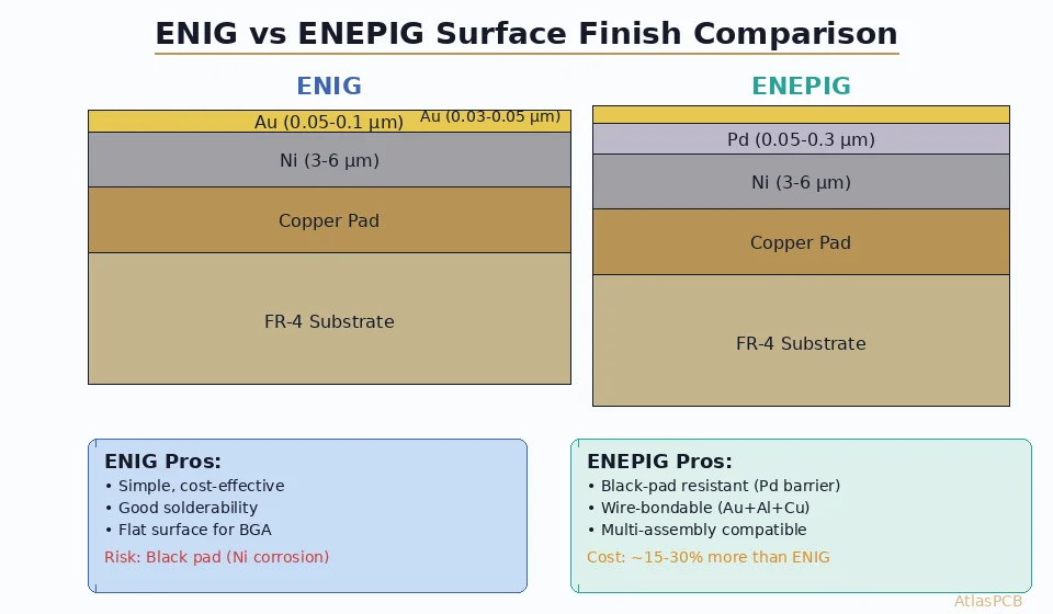
Layer Structure Comparison
Understanding what each finish actually deposits on your copper pads is essential to understanding their performance differences.
ENIG Structure
| Layer | Material | Typical Thickness | Function |
|---|---|---|---|
| Base | Copper pad | Per design | Conductor |
| Layer 1 | Electroless Nickel (Ni-P) | 3-6 µm | Barrier / solderable surface |
| Layer 2 | Immersion Gold (Au) | 0.05-0.1 µm | Oxidation protection |
Total process steps: copper activation → electroless nickel → immersion gold.
The immersion gold layer is thin by design — it exists only to protect the nickel from oxidation during storage. During soldering, gold dissolves into the solder and the joint forms between tin and nickel.
ENEPIG Structure
| Layer | Material | Typical Thickness | Function |
|---|---|---|---|
| Base | Copper pad | Per design | Conductor |
| Layer 1 | Electroless Nickel (Ni-P) | 3-6 µm | Barrier layer |
| Layer 2 | Electroless Palladium (Pd) | 0.05-0.15 µm | Barrier / bonding surface |
| Layer 3 | Immersion Gold (Au) | 0.03-0.08 µm | Oxidation protection |
Total process steps: copper activation → electroless nickel → electroless palladium → immersion gold.
The palladium layer is the critical differentiator. It serves as both a diffusion barrier between nickel and gold, and as a bonding surface for wire bonding applications.
The Black Pad Problem
Black pad is ENIG’s Achilles heel, and it is the primary technical driver for ENEPIG adoption.
Root Cause
During immersion gold deposition, gold ions displace nickel atoms through a galvanic exchange reaction:
Ni → Ni²⁺ + 2e⁻ (nickel dissolves) Au³⁺ + 3e⁻ → Au (gold deposits)
When this exchange becomes too aggressive — due to bath chemistry imbalance, excessive dwell time, or high nickel phosphorus content — the nickel surface corrodes unevenly. The result is a phosphorus-rich, amorphous nickel layer at the interface that is brittle, non-wettable, and mechanically weak.
Detection Difficulty
Black pad defects are invisible during incoming inspection. The gold layer looks normal. The defect only manifests during soldering or, worse, as a field failure months or years later. X-ray inspection cannot detect it. Cross-sectioning is the only reliable verification method, but it is destructive and impractical for production screening.
Failure Mode
Solder joints formed over black pad appear normal during initial inspection but have reduced mechanical strength. Under thermal cycling or mechanical shock, the joint fractures at the brittle nickel-gold interface — not through the solder bulk, as would be expected. Failure analysis reveals a dark, corroded nickel surface, giving the defect its name.
Industry Incidence
Conservative estimates place black pad occurrence at 1-5% of ENIG boards industry-wide, but the rate varies enormously by plating house. Shops with tight process control may see near-zero rates; shops with poorly maintained baths may see 10%+ rates. The unpredictability is the core problem.
How ENEPIG Eliminates Black Pad
The electroless palladium layer in ENEPIG is deposited onto the nickel using an autocatalytic process — not an exchange reaction. This means the nickel surface is not attacked during palladium deposition.
The subsequent immersion gold layer is deposited onto palladium, not nickel. Palladium is far more noble than nickel, so the galvanic exchange is much less aggressive. The result is a gold layer that protects the palladium without corroding it.
During soldering, gold dissolves into the solder first, then palladium dissolves, and the solder joint ultimately forms between tin and nickel — but through an intact, un-corroded nickel surface.
Performance Comparison
Solderability
| Parameter | ENIG | ENEPIG |
|---|---|---|
| Initial wetting | Excellent | Excellent |
| After 3x reflow | Good | Excellent |
| After 6x reflow | Degraded | Good |
| Shelf life (solderability) | 12 months | 12+ months |
| Black pad risk | 1-5% | Eliminated |
Both finishes offer excellent initial solderability. The difference appears after multiple thermal exposures, where ENEPIG’s palladium barrier maintains surface integrity better than ENIG’s thin gold-over-nickel structure.
Wire Bonding
| Parameter | ENIG | ENEPIG |
|---|---|---|
| Gold wire bonding | Poor | Good |
| Aluminum wire bonding | Not supported | Excellent |
| Pull strength (25µm Al) | N/A | >3.5 gf typical |
| Bond pad shear | N/A | >15 gf typical |
Wire bonding is ENEPIG’s strongest differentiator. If your design includes any wire-bonded components (COB, bare die, certain sensors), ENEPIG is mandatory.
Signal Integrity
| Parameter | ENIG | ENEPIG |
|---|---|---|
| Contact resistance | Low | Slightly lower |
| Insertion loss impact | Negligible at <6GHz | Negligible at <6GHz |
| Press-fit connector compatibility | Good | Good |
| Switch/connector cycling | Good | Excellent |
For most RF applications below 6GHz, the signal integrity difference between ENIG and ENEPIG is negligible. Above 10GHz, the additional palladium layer can marginally improve contact surface stability for gold-plated connector interfaces.
Cost Analysis
Per-Board Cost Differential
ENEPIG typically costs 15-30% more than ENIG, but the absolute cost difference depends on board complexity and panel utilization.
| Board Type | ENIG Adder | ENEPIG Adder | Delta |
|---|---|---|---|
| Simple 2L (100×100mm) | ~$0.40/board | ~$0.55/board | +$0.15 |
| 6L HDI (150×100mm) | ~$1.80/board | ~$2.30/board | +$0.50 |
| 12L complex (200×150mm) | ~$4.50/board | ~$5.80/board | +$1.30 |
These are approximate adders relative to HASL. Actual pricing varies by manufacturer and volume.
Total Cost of Ownership
The raw per-board premium for ENEPIG must be weighed against:
- Black pad failure cost: A single field failure investigation typically costs $5,000-$50,000 in engineering time, customer communication, and corrective action
- Rework cost: Black pad boards cannot be reworked — the entire board must be scrapped
- Multiple reflow tolerance: Boards requiring 3+ reflow cycles are at higher black pad risk with ENIG
For high-reliability applications, ENEPIG’s premium is typically less than 1% of total assembly cost — trivial insurance against black pad risk.
Decision Framework
Choose ENIG When
- SMT-only assembly with standard pitch components (≥0.5mm BGA pitch)
- ≤2 reflow cycles in total assembly process
- Cost-sensitive applications where black pad risk is acceptable
- Standard commercial/consumer products where field failure cost is manageable
- Your plating house has proven ENIG process control with documented low black pad rates
Choose ENEPIG When
- Wire bonding is required (any type — gold or aluminum)
- Mixed technology — SMT + wire bonding on the same board
- Ultra-fine pitch BGA (≤0.4mm) where surface planarity is critical
- Multiple reflow cycles (≥3) increase black pad risk
- High-reliability applications — medical devices, aerospace, automotive safety systems
- Long field life requirements — infrastructure, industrial controls (10+ year service life)
- Zero tolerance for black pad — when a single field failure is unacceptable
The Gray Zone
For boards that fall between these clear cases — standard BGA pitch, 2-3 reflow cycles, moderate reliability requirements — the decision often comes down to your manufacturer’s ENIG process maturity. A manufacturer with excellent ENIG controls may give you better results with ENIG than a different manufacturer would with ENEPIG.
At Atlas PCB, our partner facilities maintain tight SPC on both ENIG and ENEPIG lines. We can advise on which finish is appropriate based on your specific design requirements and assembly process.
Specification Checklist
When specifying either finish, include these parameters in your fabrication notes:
ENIG
Surface Finish: ENIG per IPC-4552 Rev B
Nickel thickness: 3-6 µm (mid-phosphorus, 6-9% P)
Gold thickness: 0.05-0.10 µm
Solderability: J-STD-003, Category 3
ENEPIG
Surface Finish: ENEPIG per IPC-4556
Nickel thickness: 3-6 µm (mid-phosphorus, 6-9% P)
Palladium thickness: 0.05-0.15 µm
Gold thickness: 0.03-0.08 µm
Wire bonding: [specify if required — Al or Au, wire diameter]
Frequently Asked Questions
Can I switch from ENIG to ENEPIG without redesigning my board?
Yes. ENEPIG is a direct drop-in replacement for ENIG with identical pad geometry and soldermask requirements. No layout changes, no stackup changes, no BOM changes. The only difference is a line item change in your fabrication specification. Solder paste, reflow profiles, and inspection criteria remain the same.
Does ENEPIG affect impedance-controlled traces?
No. Surface finish is applied only to exposed copper pads, not to internal traces or covered traces under soldermask. Impedance-controlled traces are embedded in the stackup and unaffected by surface finish selection. The only potential interaction is on exposed copper test points used for impedance verification — but this is a measurement artifact, not a design impact.
Are there applications where neither ENIG nor ENEPIG is the right choice?
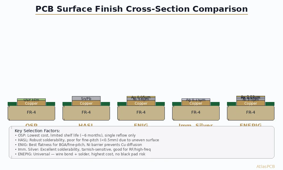
Yes. For press-fit connector applications with heavy insertion forces, hard electrolytic gold (1-2µm) is preferred over both ENIG and ENEPIG. For high-frequency edge connectors, hard gold over nickel is standard. For cost-sensitive consumer electronics with simple assembly, HASL or OSP may be more appropriate. For soldering-only applications requiring maximum shelf life at minimum cost, immersion tin or immersion silver are also viable.
Further Reading
- [HDI PCB Design Guide: Stackup Rules, Via Structures & DFM Checklist]/blog/hdi-pcb-design-guide/)
- [High-Speed PCB Design: Signal Integrity Essentials for Modern Electronics]/blog/high-speed-pcb-design/)
- [PCB Surface Finish Guide: HASL, ENIG, OSP and More Compared]/blog/pcb-surface-finish-guide/)
About AtlasPCB — We specialize in complex PCB manufacturing for HDI, RF, and high-reliability applications. Explore our HDI PCB manufacturing capabilities, RF and high-frequency PCB services, or get an full PCB manufacturing capabilities . Every order includes free engineering review. Get your quote.
Reviewed by AtlasPCB Engineering Team — IPC-certified manufacturing specialists with 15+ years of production experience in HDI, RF, and high-reliability PCB fabrication. Content based on factory floor data and real customer design reviews.
- ENEPIG
- ENIG
- surface finish
- pcb manufacturing
- wire bonding
- BGA