· AtlasPCB Engineering · Engineering · 5 min read
PCB Surface Finish Guide: HASL, ENIG, OSP and More Compared
A comprehensive comparison of PCB surface finishes including HASL, lead-free HASL, ENIG, OSP, Immersion Silver, Immersion Tin, and ENEPIG — their pros, cons, costs, and best applications.

The surface finish on a PCB protects exposed copper pads from oxidation and ensures reliable soldering during assembly. Choosing the wrong finish can lead to solderability issues, reduced shelf life, or unnecessary cost. This guide compares the most common surface finishes to help you select the right one.
Why Surface Finish Matters
Bare copper oxidizes rapidly when exposed to air. Within hours, a thin oxide layer forms that can impair solderability. The surface finish serves three purposes:
- Protect copper from oxidation during storage and handling
- Ensure solderability during component assembly
- Provide a reliable contact surface for connectors, test points, and wire bonding
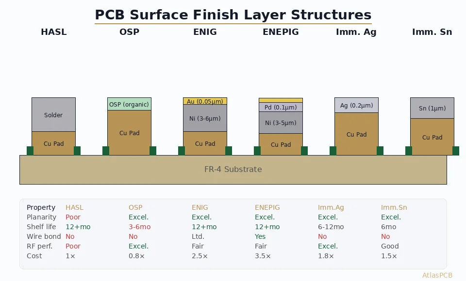
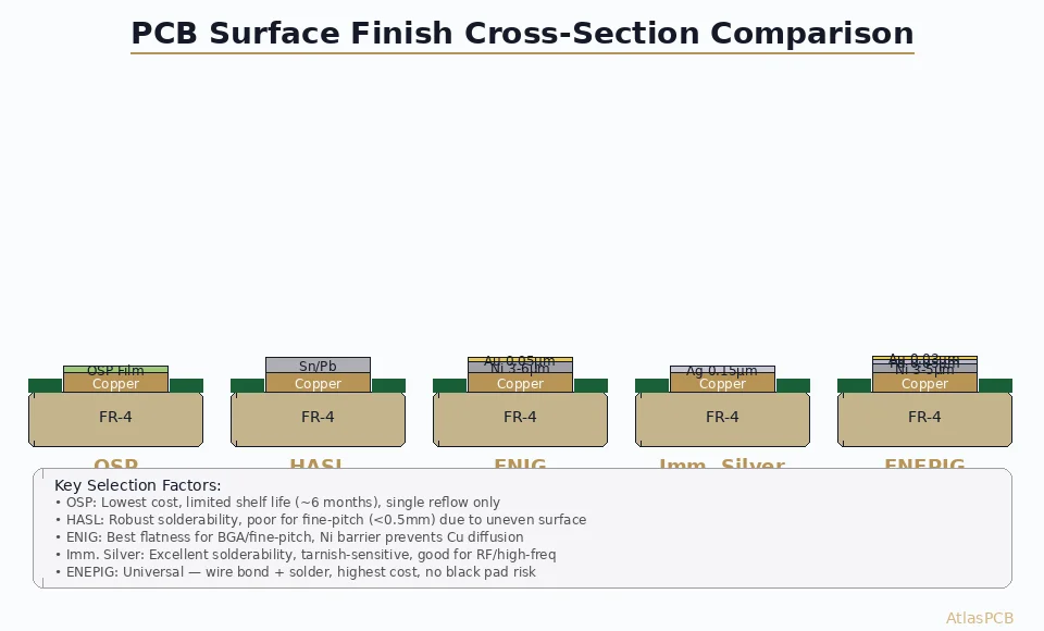
HASL (Hot Air Solder Leveling)
Process
The board is dipped into a bath of molten tin-lead solder (63Sn/37Pb), then excess solder is blown off with hot air knives, leaving a thin, even solder coating on all exposed pads.
Advantages
- Excellent solderability — the pad surface is already solder
- Long shelf life — 12+ months
- Lowest cost among all finishes
- Reworkable — easy to rework and resolder
- Proven reliability — decades of industry experience
Disadvantages
- Uneven surface — solder tends to dome on pads, making it unsuitable for fine-pitch SMD components (< 0.5mm pitch)
- Thermal shock — the high-temperature dipping process (250°C+) can stress the board
- Contains lead — not RoHS compliant (standard HASL)
- Not suitable for HDI — poor coplanarity for BGA and QFN pads
Best For
- Through-hole heavy designs
- Cost-sensitive consumer products
- Prototyping where surface flatness is not critical
Lead-Free HASL
Same process as standard HASL but uses a lead-free alloy (typically SAC305: 96.5Sn/3.0Ag/0.5Cu) with a higher melting point (~217°C vs ~183°C for SnPb).
Advantages
- RoHS compliant
- Good solderability and shelf life
- Low cost
Disadvantages
- Higher process temperature increases thermal stress
- Surface coplanarity slightly worse than standard HASL
- Still not ideal for fine-pitch components
ENIG (Electroless Nickel / Immersion Gold)
Process
A 3-6 um layer of electroless nickel is deposited on the copper, followed by a thin 0.05-0.1 um layer of immersion gold. The gold protects the nickel from oxidation; the nickel provides the solderable surface.
Advantages
- Excellent surface flatness — ideal for fine-pitch SMD, BGA, and QFN
- Long shelf life — 12+ months
- Good for wire bonding (aluminum wire)
- RoHS compliant
- Consistent pad coplanarity — critical for automated assembly
- Good corrosion resistance
Disadvantages
- Higher cost — typically 2-3x the cost of HASL
- Black pad risk — a rare nickel corrosion defect that can cause brittle solder joints (mitigated by proper process control)
- Signal loss at high frequencies — the nickel layer is magnetic and can increase insertion loss in RF applications
- Not ideal for press-fit connectors — nickel hardness can cause issues
Best For
- Fine-pitch SMD and BGA assemblies
- Products requiring long storage before assembly
- Mixed technology boards (SMD + through-hole)
- Consumer electronics, medical devices
OSP (Organic Solderability Preservative)
Process
A thin (0.2-0.5 um) organic compound (typically benzimidazole) is applied to the copper surface through a chemical bath. It provides a temporary protective coating.
Advantages
- Flat copper surface — ideal for fine-pitch components
- Lowest cost flat finish option
- Environmentally friendly — no metals involved
- Simple process — easy rework by cleaning and recoating
- Good for high-frequency — no additional metal layers to affect signal
Disadvantages
- Short shelf life — 6 months maximum, sensitive to humidity
- Limited reflow cycles — typically only 2-3 reflow passes before the coating degrades
- Not suitable for through-hole — wave soldering damages the coating
- Handling sensitive — fingerprints can damage the coating
- Not visible — difficult to inspect pad coverage visually
Best For
- High-volume SMD-only production with short storage times
- High-frequency/RF applications where ENIG’s nickel layer is problematic
- Cost-sensitive designs requiring flat pads
Immersion Silver
Process
A 0.1-0.4 um layer of silver is deposited on the copper through a chemical displacement reaction.
Advantages
- Excellent solderability and wetting
- Very flat surface — good for fine-pitch
- Good for high-frequency — silver has the highest conductivity of any metal
- RoHS compliant
- Lower cost than ENIG
Disadvantages
- Tarnish sensitive — silver tarnishes when exposed to sulfur compounds in air
- Moderate shelf life — 6-12 months in proper packaging
- Handling sensitive — requires gloves; skin oils cause tarnishing
- Micro-voiding risk — small voids can form in solder joints (manageable with proper reflow profiles)
Best For
- High-frequency/RF applications
- EMI shielding (silver’s conductivity helps)
- Membrane switches and dome contacts
Immersion Tin
Process
A ~1 um layer of tin is chemically deposited on the copper surface.
Advantages
- Flat surface — good coplanarity
- Good solderability for tin-lead and lead-free solders
- Compatible with press-fit connectors
- RoHS compliant
- Moderate cost
Disadvantages
- Tin whisker risk — tin can grow microscopic whiskers that cause short circuits (mitigated by process controls)
- Short shelf life — 6 months; tin intermetallic growth over time
- Handling sensitive — requires gloves
- Multiple reflow limitations — tin diffuses into copper after first reflow
Best For
- Press-fit connector applications
- Backplanes
- Cost-effective flat finish where ENIG is too expensive
ENEPIG (Electroless Nickel / Electroless Palladium / Immersion Gold)
Process
Similar to ENIG but adds a 0.05-0.15 um palladium layer between nickel and gold. Layering: Cu → Ni (3-5 um) → Pd (0.05-0.15 um) → Au (0.03-0.05 um).
Advantages
- Eliminates black pad risk (palladium acts as a barrier)
- Excellent for gold wire bonding and aluminum wire bonding
- Universal finish — compatible with all soldering and bonding methods
- Best shelf life and reliability
Disadvantages
- Highest cost — palladium is expensive
- Limited supplier availability — not all fabricators offer this finish
Best For
- Wire bonding applications (gold and aluminum wire)
- High-reliability products (aerospace, medical implants)
- Mixed assembly with both soldering and wire bonding
Comparison Summary
| Finish | Flatness | Shelf Life | Cost | Fine-Pitch | RoHS | RF/HF |
|---|---|---|---|---|---|---|
| HASL (SnPb) | Poor | 12+ mo | Lowest | No | No | Fair |
| Lead-free HASL | Poor | 12+ mo | Low | No | Yes | Fair |
| ENIG | Excellent | 12+ mo | High | Yes | Yes | Fair |
| OSP | Excellent | 6 mo | Lowest | Yes | Yes | Best |
| Imm. Silver | Excellent | 6-12 mo | Medium | Yes | Yes | Very Good |
| Imm. Tin | Good | 6 mo | Medium | Yes | Yes | Good |
| ENEPIG | Excellent | 12+ mo | Highest | Yes | Yes | Fair |
Conclusion
There is no single “best” surface finish — the right choice depends on your component types, assembly process, storage requirements, operating frequency, and budget. For general purpose SMD designs, ENIG offers the best balance of reliability and manufacturability. For cost-sensitive high-volume production, lead-free HASL or OSP may be more appropriate. For RF/high-frequency applications, OSP or immersion silver is preferred due to the absence of magnetic nickel layers.
Further Reading
[HDI PCB Design Guide: Stackup Rules, Via Structures & DFM Checklist]/blog/hdi-pcb-design-guide/)
[ENEPIG vs ENIG: Which PCB Surface Finish for Your Design?]/blog/enepig-vs-enig/)
[EMC/EMI Design for PCBs: Passing Compliance on the First Try]/blog/emc-emi-pcb-design/)
[IPC Class 3 Requirements: The Complete Guide for Designers]/blog/ipc-class-3-requirements/)
About AtlasPCB — We specialize in complex PCB manufacturing for HDI, RF, and high-reliability applications. Explore our RF and high-frequency PCB services, or get an full PCB manufacturing capabilities . Every order includes free engineering review. Get your quote.
Reviewed by AtlasPCB Engineering Team — IPC-certified manufacturing specialists with 15+ years of production experience in HDI, RF, and high-reliability PCB fabrication. Content based on factory floor data and real customer design reviews.
- surface finish
- ENIG
- HASL
- OSP