· AtlasPCB Engineering · Engineering · 5 min read
PCB Via Types: Through-Hole, Blind, Buried, and Microvias Explained
Understand all PCB via types — through-hole, blind, buried, microvia, and via-in-pad. Learn their construction, aspect ratios, cost implications, and when to use each type.

Vias are the vertical connections that link copper traces on different PCB layers. Choosing the right via type affects routing density, signal integrity, manufacturing cost, and board reliability. This guide explains each via type and when to use it.
Through-Hole Via (Standard Via)
Description
A plated hole that passes through ALL layers of the PCB, from top to bottom. The most common and least expensive via type.
Specifications
- Drill diameter: 0.2-0.5mm (8-20 mil) typical
- Pad diameter: 0.4-0.8mm (drill + 2x annular ring)
- Aspect ratio: Up to 8:1 standard (10:1 advanced)
- Plating thickness: 20-25um copper minimum
Advantages
- Lowest cost — standard drilling process
- Highest reliability — full barrel plating
- No special manufacturing required
- Good current carrying capacity
Disadvantages
- Consumes routing space on ALL layers (the hole passes through every layer)
- Creates stub length on unused layers, causing signal integrity issues at high frequencies
- Limits component placement density
Best For
- General purpose routing
- 2-layer and 4-layer boards
- Through-hole component connections
- Power and ground connections
Blind Via
Description
A plated hole that connects an outer layer to one or more inner layers, but does NOT pass through the entire board. Visible only from one side.
Specifications
- Drill diameter: 0.1-0.3mm
- Depth: 1-3 layers deep (from outer layer)
- Aspect ratio: Typically ≤1:1 for laser-drilled, up to 1:1.2
- Manufacturing: Laser drilling (microvia) or controlled-depth mechanical drilling
Advantages
- Saves routing space on layers it doesn’t penetrate
- Reduces stub length for better signal integrity
- Enables higher routing density
Disadvantages
- Requires sequential lamination (adds processing steps)
- Higher cost than through-hole vias
- Depth control is critical — requires process precision
- Limited number of layers it can connect
Best For
- HDI designs requiring high routing density
- Fine-pitch BGA breakout
- Signal integrity improvement (reducing stubs)
Buried Via
Description
A plated hole that connects two or more INNER layers but does NOT reach either outer surface. Completely hidden inside the board.
Specifications
- Drill diameter: 0.15-0.3mm
- Connection: Inner layer to inner layer only
- Manufacturing: Drilled and plated before lamination of outer layers
Advantages
- Maximum routing space preservation on outer layers
- No impact on component placement
- Excellent for dense multi-layer designs
Disadvantages
- Most expensive via type for conventional PCBs
- Requires separate drilling and plating cycle
- Must be manufactured before final lamination
- Registration between buried via layers is critical
Best For
- Complex multi-layer boards (8+ layers)
- Designs where outer layer routing space is premium
- High-density signal routing between inner layers

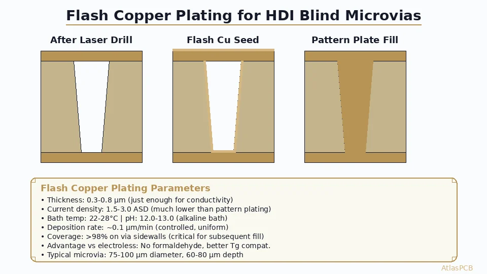
Microvia
Description
A very small via (≤150um / 6mil diameter) typically laser-drilled, connecting adjacent layers. The defining feature of HDI PCBs.
Specifications
- Drill diameter: 75-150um (3-6 mil)
- Pad diameter: 200-350um (8-14 mil)
- Depth: Single layer span (adjacent layers only)
- Aspect ratio: ≤1:1 for reliable plating
- Manufacturing: CO2 or UV laser drilling
Types of Microvia Arrangements
Stacked Microvias:
- Multiple microvias directly aligned on consecutive layers
- Each via is copper-filled before the next buildup layer is laminated
- Maximum density but highest cost
- Required for fine-pitch BGA (<0.5mm) breakout
Staggered Microvias:
- Microvias on consecutive layers are offset from each other
- Don’t require copper fill
- Lower cost than stacked
- Use more routing space due to offset
Skip Microvias:
- Single via spans two dielectric layers instead of one
- More difficult to manufacture reliably
- Not recommended for most designs
Advantages
- Smallest via footprint — maximum routing density
- Excellent signal integrity (minimal stub, low inductance)
- Enables fine-pitch BGA breakout (0.3-0.5mm pitch)
- Can be placed directly in pads (via-in-pad)
Disadvantages
- Requires HDI manufacturing (higher base cost)
- Limited to single-layer span (unless stacked)
- Copper fill adds cost for stacked configurations
- Not all fabricators have laser drilling capability
Best For
- Smartphone and tablet PCBs
- Fine-pitch BGA breakout
- High-speed serial interfaces
- Any design requiring maximum density
Via-in-Pad
Description
A via placed directly within an SMD pad, rather than routed to the via through a trace. Can use any via type (through-hole, blind, or microvia).
Why Via-in-Pad?
- BGA breakout: The only way to route inner BGA balls on fine-pitch packages
- Thermal performance: Direct thermal path from component pad to inner copper planes
- Shorter trace length: Signal goes straight down, minimizing trace stub
Requirements
- Via MUST be filled (non-conductive epoxy or copper fill) and cap-plated
- If not filled, solder will wick into the via during reflow, creating a void and weak solder joint
- Planarized surface required for reliable solder paste printing
Cost Impact
- Via fill and cap plating adds $1-5 per board (depending on via count)
- Essential for BGA pitch ≤0.65mm
Via Comparison Summary
| Feature | Through-Hole | Blind | Buried | Microvia |
|---|---|---|---|---|
| Drill size | 0.2-0.5mm | 0.1-0.3mm | 0.15-0.3mm | 0.075-0.15mm |
| Pad size | 0.4-0.8mm | 0.3-0.6mm | 0.35-0.6mm | 0.2-0.35mm |
| Layers connected | All | Outer to inner | Inner to inner | Adjacent only |
| Aspect ratio | ≤8:1 | ≤1:1.2 | ≤8:1 | ≤1:1 |
| Manufacturing | Standard | Sequential lam | Pre-lamination | HDI/Laser |
| Cost impact | Baseline | +20-40% | +30-50% | +30-50% |
| Signal integrity | Fair (stub) | Good | Good | Best |
| Density impact | Low | Medium | Medium | Highest |
Choosing the Right Via Type
- Start with through-hole vias — they’re cheapest and most reliable
- Use blind vias when through-hole routing is too dense or stubs cause SI problems
- Use buried vias when inner layer routing space is critical
- Use microvias when component pitch demands it or signal integrity requirements are extreme
- Always discuss via strategy with your fabricator early in the design process
Conclusion
Via selection directly impacts PCB cost, manufacturability, and performance. Most designs can use through-hole vias exclusively. As density and speed requirements increase, blind vias and microvias become necessary. Understanding each via type’s capabilities and limitations ensures you choose the most cost-effective solution for your specific design requirements.
Further Reading
[HDI PCB Design Guide: Stackup Rules, Via Structures & DFM Checklist]/blog/hdi-pcb-design-guide/)
[HDI PCB Technology: Microvias, Laser Drilling, and High-Density Design]/blog/hdi-pcb-technology/)
[PCB Sequential Lamination: Process, Design Rules, and When You Need It]/blog/pcb-sequential-lamination/)
[Via-in-Pad Design: Filled, Capped, and Plated Over — Complete Guide]/blog/via-in-pad-design/)
[Blind Via vs Buried Via: Design Rules, Cost Impact & When to Use Each]/blog/blind-via-vs-buried-via/)
[High-Speed PCB Design: Signal Integrity Essentials for Modern Electronics]/blog/high-speed-pcb-design/)
[BGA Escape Routing: Strategies for 0.4mm, 0.5mm, and 0.8mm Pitch]/blog/bga-escape-routing/)
About AtlasPCB — We specialize in complex PCB manufacturing for HDI, RF, and high-reliability applications. Explore our HDI PCB manufacturing capabilities . Every order includes free engineering review. Get your quote.
Reviewed by AtlasPCB Engineering Team — IPC-certified manufacturing specialists with 15+ years of production experience in HDI, RF, and high-reliability PCB fabrication. Content based on factory floor data and real customer design reviews.
- pcb vias
- blind via
- buried via
- microvia
- via-in-pad