· AtlasPCB Engineering · Engineering · 5 min read
PCB Stackup Design: Best Practices for Signal Integrity and EMI Control
Master PCB stackup design — understand symmetric construction, signal-ground pairing, common 4/6/8-layer stackups, material selection, impedance impact, and EMI reduction strategies.

The PCB stackup — the arrangement of copper and dielectric layers — is one of the most critical decisions in board design. A well-designed stackup ensures controlled impedance, minimizes EMI, provides adequate power delivery, and maintains manufacturability.
Stackup Design Principles
1. Symmetry
The stackup must be symmetric about the center to prevent warping during lamination and reflow. Asymmetric stackups cause the board to bow or twist due to uneven thermal expansion.
2. Signal-Ground Pairing
Every signal layer should be adjacent to a ground (or power) plane. This provides:
- Low-impedance return path for signals
- Controlled impedance (trace geometry referenced to plane)
- EMI shielding (plane acts as a shield)
3. Plane Separation
Ground and power planes should be placed adjacent to each other with thin dielectric between them for maximum decoupling capacitance.
4. High-Speed Signals on Inner Layers
Route high-speed signals as striplines (between two ground planes) rather than microstrips (outer layers). Striplines have lower radiation and better shielding.
Common Stackup Configurations
4-Layer Standard (Most Popular)
Layer 1: Signal (Top)          — Microstrip
         Prepreg (~0.2mm)
Layer 2: Ground Plane          — Reference for L1
         Core (~1.0mm)
Layer 3: Power Plane           — Reference for L4
         Prepreg (~0.2mm)
Layer 4: Signal (Bottom)       — Microstrip
Total thickness: ~1.6mm Advantages: Two dedicated planes, good impedance control, low cost Limitations: Only 2 routing layers; ground and power separated by thick core
4-Layer High-Speed Variant
Layer 1: Signal + Power (Top)
         Prepreg (~0.1mm, thin)
Layer 2: Ground Plane
         Core (~1.2mm)
Layer 3: Ground Plane
         Prepreg (~0.1mm, thin)
Layer 4: Signal + Power (Bottom)
Advantages: Both signal layers have adjacent ground plane; GND-GND pair provides excellent decoupling Limitations: No dedicated power plane; power must be routed as traces or split planes on signal layers
6-Layer Standard
Layer 1: Signal (Top)
         Prepreg
Layer 2: Ground Plane
         Core
Layer 3: Signal (Inner)
         Prepreg
Layer 4: Signal (Inner)
         Core
Layer 5: Power Plane
         Prepreg
Layer 6: Signal (Bottom)
Advantages: 3 routing layers; L1 and L6 reference ground/power planes Concern: L3 and L4 reference each other (not ideal for controlled impedance)
6-Layer Improved
Layer 1: Signal (Top)
         Prepreg (~0.1mm)
Layer 2: Ground Plane
         Core (~0.3mm)
Layer 3: Signal (Inner)
         Core (~0.3mm)
Layer 4: Power Plane
         Core (~0.3mm)
Layer 5: Signal (Inner)
         Prepreg (~0.1mm)
Layer 6: Ground Plane → Signal (Bottom)
Better version: L3 references L2 (ground), L5 references L6 — but L6 doubles as signal+ground
8-Layer Recommended
Layer 1: Signal (Top)
         Prepreg (~0.1mm)
Layer 2: Ground Plane
         Core (~0.3mm)
Layer 3: Signal (Inner)
         Prepreg (~0.2mm)
Layer 4: Power Plane
         Core (~0.3mm)
Layer 5: Ground Plane
         Prepreg (~0.2mm)
Layer 6: Signal (Inner)
         Core (~0.3mm)
Layer 7: Ground Plane
         Prepreg (~0.1mm)
Layer 8: Signal (Bottom)
Advantages: Every signal layer adjacent to a plane; GND-PWR and GND-GND pairs for excellent decoupling; best EMI performance in 8 layers

Material Selection
Core and Prepreg
| Material | Dk | Dk Tolerance | Loss (Df) | Use Case |
|---|---|---|---|---|
| Standard FR-4 | 4.2-4.8 | +/-10% | 0.015-0.025 | General purpose |
| Mid-Tg FR-4 | 4.2-4.5 | +/-8% | 0.015-0.020 | Lead-free assembly |
| High-Tg FR-4 | 4.0-4.4 | +/-5% | 0.010-0.015 | High reliability |
| Low-loss (Megtron/Panasonic) | 3.4-3.8 | +/-3% | 0.003-0.005 | High-speed >10Gbps |
| PTFE/Rogers | 2.2-3.5 | +/-2% | 0.001-0.003 | RF/Microwave |
Prepreg Styles
| Style | Glass Content | Thickness (cured) | Dk |
|---|---|---|---|
| 1080 | Low | 65um | Lower (more resin) |
| 2116 | Medium | 120um | Medium |
| 7628 | High | 185um | Higher (more glass) |
Key insight: Dk varies with glass content. Areas over glass bundles have different Dk than areas over resin. This “fiber weave effect” causes impedance variation in high-speed designs. Mitigation: use spread glass or route traces at angles to the weave.
Impedance Impact
Stackup directly determines impedance. The critical parameters are:
- Dielectric thickness (H): Distance from signal trace to reference plane. Thinner = lower impedance (for same trace width).
- Dielectric constant (Dk): Higher Dk = lower impedance.
- Trace width (W): Wider trace = lower impedance.
- Copper thickness (T): Thicker copper slightly lowers impedance.
Common Impedance Targets
| Interface | Impedance | Trace Type |
|---|---|---|
| General GPIO | 50-60 ohm SE | Microstrip or Stripline |
| DDR4 data | 40 ohm SE | Stripline preferred |
| USB 2.0 | 90 ohm diff | Differential pair |
| USB 3.0 | 85 ohm diff | Differential pair |
| HDMI | 100 ohm diff | Differential pair |
| PCIe | 85 ohm diff | Differential pair (stripline) |
| Ethernet | 100 ohm diff | Differential pair |
| 50 ohm RF | 50 ohm SE | Microstrip (outer) |
EMI Considerations
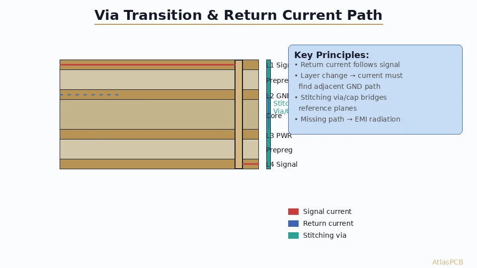
Ground Plane Continuity
- Never cut slots or splits in ground planes under high-speed traces
- Return current follows the path directly beneath the signal trace
- A slot forces return current to detour, creating a radiating loop antenna
Via Stitching
- Place ground vias near signal vias (especially at layer transitions)
- Via stitching around board edges creates a Faraday cage effect
- Via pitch for stitching: <= lambda/20 at the highest frequency of concern
Power Plane Design
- Use decoupling capacitor placement strategy: bulk caps near power entry, ceramic caps near IC pins
- Adjacent GND-PWR plane pair acts as a distributed capacitor
- Thin dielectric between GND and PWR planes (2-4 mil) maximizes decoupling
Working With Your Manufacturer
- Request their standard stackup options — using standard stackups saves cost and lead time
- Provide impedance targets — they will calculate trace widths for you
- Confirm material availability — not all dielectric thicknesses and materials are in stock
- Review the stackup drawing — verify symmetry, dielectric thicknesses, and copper weights before production
- Iterate if needed — stackup optimization may require 2-3 rounds of discussion
Conclusion
Stackup design is the foundation of signal integrity and EMI performance. Follow the core principles — symmetry, signal-ground pairing, and appropriate material selection — and your boards will perform reliably. Start with your manufacturer’s standard stackup options and customize only when your design requirements demand it. The few hours invested in stackup optimization prevent countless hours of debugging signal integrity and EMI problems.
Further Reading
[Controlled Impedance PCB: Design, Stackup & Testing Explained]/blog/controlled-impedance-pcb/)
[Differential Pair Routing: Rules, Impedance Control, and Layout Best Practices]/blog/differential-pair-routing-pcb/)
[Microstrip vs Stripline: Routing Strategies for Controlled Impedance PCBs]/blog/microstrip-vs-stripline/)
[High-Speed PCB Design: Signal Integrity Essentials for Modern Electronics]/blog/high-speed-pcb-design/)
[High-Multilayer FR4 vs Standard FR4: When to Upgrade Material Grade]/blog/high-multilayer-fr4-vs-standard-fr4/)
[HDI PCB Design Guide: Stackup Rules, Via Structures & DFM Checklist]/blog/hdi-pcb-design-guide/)
[Multilayer PCB Stackup Design Guide: 8 to 30+ Layers Step by Step]/blog/multilayer-pcb-stackup-design-guide/)
[PCB Manufacturer with Engineering Review: Why Human DFM Audit Matters]/blog/pcb-manufacturer-engineering-review/)
[EMC/EMI Design for PCBs: Passing Compliance on the First Try]/blog/emc-emi-pcb-design/)
[PCB Grounding Techniques: Star, Split, and Solid Ground Plane Strategies]/blog/pcb-grounding-techniques/)
About AtlasPCB — We specialize in complex PCB manufacturing for HDI, RF, and high-reliability applications. Explore our multilayer PCB fabrication up to 30 layers . Every order includes free engineering review. Get your quote.
Reviewed by AtlasPCB Engineering Team — IPC-certified manufacturing specialists with 15+ years of production experience in HDI, RF, and high-reliability PCB fabrication. Content based on factory floor data and real customer design reviews.
- stackup design
- layer arrangement
- signal integrity
- EMI