· AtlasPCB Engineering · Engineering · 5 min read
Common PCB Defects and How to Prevent Them
Identify and prevent the most common PCB defects — solder bridges, tombstoning, cold joints, delamination, copper cracking, CAF, via failures, and DFM best practices for defect-free boards.

Even with modern manufacturing processes, PCB defects can occur at any stage — from fabrication through assembly. Understanding the most common defects, their root causes, and prevention strategies is key to achieving high yields and reliable products.
Fabrication Defects
1. Delamination
What it is: Separation of laminate layers, appearing as blisters or bubbles in the board.
Root causes:
- Excessive moisture absorption before lamination
- Insufficient cure temperature or pressure during lamination
- Contamination between layers
- Thermal shock during soldering (especially lead-free at 260°C+)
Prevention:
- Bake boards before assembly if stored >6 months (125°C for 2-4 hours)
- Use appropriate Tg material for the assembly process (Tg > reflow peak temp)
- Ensure proper storage conditions (dry, <30°C, <60% RH)
- Request cross-section verification from manufacturer for critical boards
2. Copper Cracking (Barrel Crack)
What it is: Cracks in the copper plating inside via barrels, causing intermittent or permanent open circuits.
Root causes:
- CTE (Coefficient of Thermal Expansion) mismatch between copper plating and FR-4 substrate in the Z-axis
- Insufficient copper plating thickness (<20um)
- Excessive thermal cycling
- Poor plating adhesion
Prevention:
- Specify minimum 25um copper plating for Class 3 boards
- Use high-Tg materials to reduce Z-axis expansion
- Minimize thermal shock during assembly
- Request thermal stress testing (solder float at 288°C for 10s)
3. CAF (Conductive Anodic Filament)
What it is: Electrochemical growth of conductive copper filaments along glass fibers between conductors, causing short circuits.
Root causes:
- Moisture penetration along glass fiber bundles
- Voltage bias between adjacent conductors
- High humidity operating environment
- Poor resin-to-glass adhesion in the laminate
Prevention:
- Use CAF-resistant laminate materials
- Increase spacing between vias and between vias and traces
- Avoid drilling through glass bundles (use offset drill patterns)
- Conformal coating for humidity protection
4. Under-Etching / Over-Etching
What it is: Trace widths too wide (under-etching) or too narrow (over-etching) compared to design specifications.
Root causes:
- Etchant concentration or temperature out of specification
- Inconsistent photoresist development
- Heavy copper requires longer etching (more side-etching)
Prevention:
- Specify tight trace width tolerances (+/-20% for Class 2, +/-10% for Class 3)
- Consider etch compensation in your design files
- Use manufacturer’s recommended minimum trace widths for your copper weight

Assembly Defects
5. Solder Bridges
What it is: Unintended solder connections between adjacent pads or pins.
Root causes:
- Too much solder paste (stencil aperture too large or thick)
- Insufficient solder mask dam between pads
- Paste misalignment during printing
- Component misplacement
- Inadequate reflow profile
Prevention:
- Verify stencil aperture design (area ratio >0.66)
- Ensure solder mask dam width >= 3 mil (4 mil preferred)
- Use SPI (Solder Paste Inspection) after printing
- Calibrate pick-and-place machine accuracy
- Optimize reflow profile for your paste type
6. Tombstoning
What it is: One end of a small passive component (0402, 0201) lifts off the pad during reflow, standing upright like a tombstone.
Root causes:
- Unequal solder paste volume on the two pads
- Thermal imbalance — one pad heats faster than the other
- Asymmetric copper distribution around the pads
- Component is too light relative to solder surface tension
Prevention:
- Ensure symmetric pad design — both pads identical size
- Balance copper distribution (thermal relief on both pads or neither)
- Use the same trace entry direction on both pads
- Reduce reflow heating rate to allow more even temperature distribution
- Consider using smaller stencil apertures for tiny components
7. Cold Solder Joints
What it is: Solder joint that didn’t reach proper reflow temperature, resulting in dull, grainy appearance and weak mechanical/electrical connection.
Root causes:
- Reflow peak temperature too low
- Insufficient soak time in reflow profile
- Large thermal mass component (connector, transformer) acting as heat sink
- Expired or improperly stored solder paste
Prevention:
- Verify reflow profile with thermocouple measurements
- Extend soak zone for boards with mixed thermal mass components
- Use fresh solder paste (within 6 months of manufacture)
- Ensure paste is at room temperature before use (allow 4 hours after removing from refrigerator)
8. Head-in-Pillow (BGA)
What it is: BGA solder ball makes contact with the paste but doesn’t fully collapse and merge, creating a partial solder joint.
Root causes:
- Board warpage during reflow — BGA ball lifts off paste at peak temperature, then returns during cooling but paste has already solidified
- Oxidized BGA balls or pads
- Insufficient paste volume under BGA
Prevention:
- Use low-warpage BGA substrates
- Control board warpage to <0.5% (use support fixtures in reflow oven)
- Ensure clean BGA pads (ENIG preferred for BGA sites)
- Optimize reflow profile — ensure paste and ball melt simultaneously
- X-ray inspection is the only reliable detection method
9. Voiding (BGA and Thermal Pads)
What it is: Gas bubbles trapped in solder joints, appearing as voids in X-ray images.
Root causes:
- Flux outgassing during reflow
- Moisture in the board or components
- Excessive paste volume
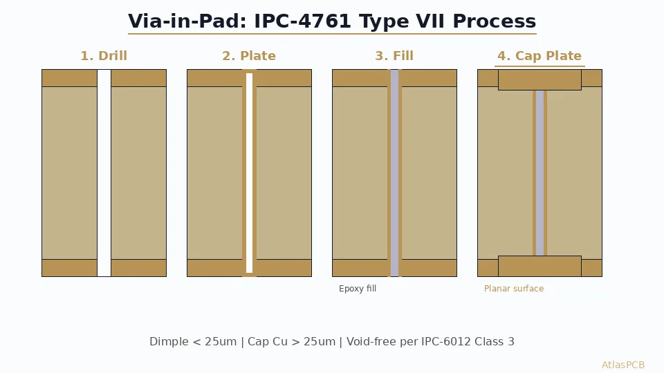
- Via-in-pad without proper filling
Prevention:
- Optimize reflow profile (adequate preheat to drive off volatiles)
- Bake moisture-sensitive components before assembly
- Use vacuum reflow for critical applications
- Fill and cap-plate via-in-pad to prevent solder wicking
Acceptable void levels: IPC-7095 recommends <25% void area for BGA balls, <50% for thermal pads.
Prevention Framework: DFM + DFA
Design for Manufacturability (DFM)
- Follow manufacturer’s minimum feature sizes (trace, space, drill, annular ring)
- Use standard stackups and materials
- Avoid acute angles in traces (acid traps)
- Provide adequate solder mask dams (>=4 mil)
- Include test points for electrical testing
Design for Assembly (DFA)
- Use NSMD pad openings for SMD components
- Symmetric pad design for passive components (anti-tombstoning)
- Adequate thermal relief on through-hole pads connected to planes
- Component spacing: >=0.5mm between components for automated assembly
- Fiducial marks for pick-and-place alignment
Conclusion
Most PCB defects are preventable through proper design, material selection, and process control. Follow DFM/DFA guidelines from your manufacturer, specify the appropriate IPC class for your reliability requirements, and implement a comprehensive test strategy (SPI, AOI, X-ray, ICT, functional test) to catch defects early. The cost of prevention is always less than the cost of field failures.
Further Reading
[Via-in-Pad Design: Filled, Capped, and Plated Over — Complete Guide]/blog/via-in-pad-design/)
[High-Multilayer FR4 vs Standard FR4: When to Upgrade Material Grade]/blog/high-multilayer-fr4-vs-standard-fr4/)
[PCB DFM Checklist: 50 Points to Review Before Sending Gerbers]/blog/pcb-dfm-checklist/)
[ENEPIG vs ENIG: Which PCB Surface Finish for Your Design?]/blog/enepig-vs-enig/)
[PCB Solder Mask: Types, Colors, and Functions Explained]/blog/pcb-solder-mask-guide/)
[PCB Surface Finish Guide: HASL, ENIG, OSP and More Compared]/blog/pcb-surface-finish-guide/)
[BGA Soldering and Rework: Challenges, Inspection, and Best Practices]/blog/bga-soldering-rework/)
[IPC Class 3 Requirements: The Complete Guide for Designers]/blog/ipc-class-3-requirements/)
[Heavy Copper PCB: Design Rules, Manufacturing Limits, and Thermal Management]/blog/heavy-copper-pcb/)
About AtlasPCB — We specialize in complex PCB manufacturing for HDI, RF, and high-reliability applications. Explore our free engineering DFM review, or get an full PCB manufacturing capabilities . Every order includes free engineering review. Get your quote.
Reviewed by AtlasPCB Engineering Team — IPC-certified manufacturing specialists with 15+ years of production experience in HDI, RF, and high-reliability PCB fabrication. Content based on factory floor data and real customer design reviews.
- pcb defects
- quality control
- troubleshooting
- DFM