· AtlasPCB Engineering · Engineering · 9 min read
Heavy Copper PCB: Design Rules, Manufacturing Limits, and Thermal Management
Complete guide to heavy copper PCB design and manufacturing. Covers copper weight definitions, etching tolerances, thermal via design, current capacity, and specification best practices for power electronics.
Heavy copper PCBs solve a fundamental problem: getting large currents and significant heat out of a circuit board without burning it up. When your design needs to handle 10A, 50A, or even 200A+, standard 1oz copper simply cannot do the job.
This guide covers the engineering principles, design rules, and manufacturing constraints you need to specify heavy copper PCBs correctly.
Copper Weight Definitions
The PCB industry classifies copper thickness by weight per square foot:
| Classification | Weight (oz/ft²) | Thickness (µm) | Thickness (mils) |
|---|---|---|---|
| Standard | 0.5 - 2 | 17 - 70 | 0.7 - 2.8 |
| Heavy copper | 3 - 10 | 105 - 350 | 4.1 - 13.8 |
| Extreme copper | 10 - 20+ | 350 - 700+ | 13.8 - 27.6+ |
The boundary between “standard” and “heavy” is generally accepted at 3oz (105µm). Above 10oz enters extreme copper territory where only a handful of manufacturers worldwide have reliable capability.
Finished vs Starting Copper
A critical specification detail: copper weight can refer to either the starting foil thickness or the finished plated thickness. In standard PCB manufacturing, 1oz starting copper gains approximately 0.5-1.0oz from electroplating during the through-hole plating process. For heavy copper, this plating contribution is proportionally smaller.
Always specify whether your copper weight requirement refers to finished minimum thickness or starting foil weight. Ambiguity here causes real yield problems.
Why Heavy Copper
Current Capacity
Copper’s current-carrying ability scales linearly with cross-sectional area. A trace in 6oz copper has 6x the cross-section of the same width trace in 1oz copper, and therefore approximately 6x the current capacity (with some non-linearity due to thermal effects).
Practical current ratings (external layer, 20°C rise, still air):
| Trace Width | 1oz | 3oz | 6oz | 10oz |
|---|---|---|---|---|
| 100mil (2.5mm) | 3.5A | 8A | 14A | 21A |
| 200mil (5mm) | 5.5A | 15A | 25A | 38A |
| 500mil (12.7mm) | 10A | 28A | 47A | 72A |
| 1000mil (25.4mm) | 15A | 42A | 72A | 110A |
These are conservative estimates based on IPC-2152 external layer charts. Internal layers carry approximately 50-60% of external layer current at the same temperature rise due to reduced heat dissipation.
Thermal Management
Heavy copper serves as an integrated heat spreader. Copper’s thermal conductivity (385 W/m·K) is roughly 1000x better than FR4 (0.3 W/m·K). Wide heavy copper planes distribute heat laterally, and heavy copper thermal vias transfer heat between layers.
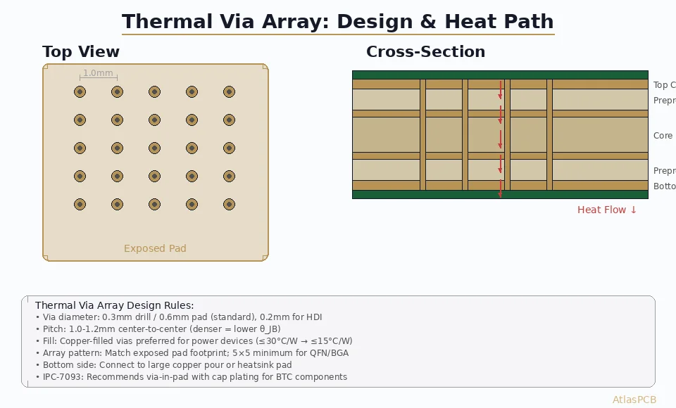
Thermal via arrays in heavy copper:
| Via Specification | Thermal Resistance (per via) |
|---|---|
| 12mil drill, 1oz plating, 62mil board | ~90°C/W |
| 12mil drill, 1oz plating, 31mil board | ~45°C/W |
| 20mil drill, 2oz plating, 62mil board | ~35°C/W |
| 20mil drill, 2oz plating, 31mil board | ~18°C/W |
A 5×5 array of 20mil heavy-plated thermal vias in a 31mil board achieves approximately 0.7°C/W — competitive with dedicated thermal interface materials.
Mechanical Strength
Heavy copper adds significant mechanical rigidity to the PCB. This matters for:
- High-vibration environments: automotive, industrial, military
- Connector retention: press-fit connectors exert significant force on through-holes
- Thermal cycling: thicker copper plating in vias improves barrel reliability through thousands of thermal cycles
Design Rules for Heavy Copper
Etch Compensation
This is the most critical design consideration. When copper is etched, the etchant attacks sideways (undercut) as well as downward. Thicker copper means more etching time, which means more undercut.
Typical etch compensation factors:
| Copper Weight | Undercut Per Side | Min Trace Width | Min Space |
|---|---|---|---|
| 1oz (35µm) | ~25µm | 3mil (75µm) | 3mil |
| 2oz (70µm) | ~50µm | 5mil (125µm) | 5mil |
| 3oz (105µm) | ~80µm | 8mil (200µm) | 8mil |
| 6oz (210µm) | ~160µm | 13mil (330µm) | 13mil |
| 10oz (350µm) | ~250µm | 20mil (500µm) | 20mil |
These are typical minimums — not design targets. Build in margin. Design to 2x these minimums whenever possible.
Trace Profile
Heavy copper traces do not have vertical sidewalls. The etching process creates a trapezoidal cross-section where the trace is wider at the bottom (closest to the substrate) and narrower at the top. For 6oz copper, the top-to-bottom width difference can be 10-12mil (250-300µm).
This trapezoidal profile affects:
- Impedance calculations: the effective trace width is the average of top and bottom widths
- Clearance calculations: use the widest dimension (bottom) for electrical clearance checks
- Solder mask registration: mask openings must account for the wider base
Soldermask Considerations
Applying soldermask over heavy copper creates unique challenges:
- Step coverage: Standard liquid photoimageable (LPI) mask struggles to cover the steep sidewalls of heavy copper traces. Voids and thin spots are common at trace edges.
- Thickness uniformity: The mask is thinner over trace tops and thicker in channels between traces.
- Cure issues: Thick mask pools between traces may not fully cure, leading to tackiness or adhesion problems.
Solutions:
- Use conformal-coat-grade soldermask designed for topography
- Specify minimum 1mil mask thickness over copper features
- Consider selective mask — mask only signal areas, leave power bus areas exposed
- For extreme copper (>10oz), plug-and-print mask application may be required
Via Design
Vias in heavy copper boards need attention:
Aspect ratio: A 12mil drill through a 125mil board with 6oz copper on each side is actually punching through ~150mil total (125mil FR4 + 2×13mil copper). The effective aspect ratio increases.
Plating distribution: Thicker starting copper means the via barrel must be plated from a deeper starting point. IPC Class 3 requires minimum 1mil (25µm) barrel plating — verify your manufacturer can achieve this uniformity in high-aspect-ratio holes with heavy copper.
Thermal relief: Heavy copper ground and power planes should always use thermal relief connections to vias, not direct connections. Without thermal relief, the massive copper heat sink makes hand soldering impossible and can cause problems even for wave soldering.

Mixed Copper Construction
The most cost-effective approach for boards that need both power handling and signal integrity is mixed copper construction.
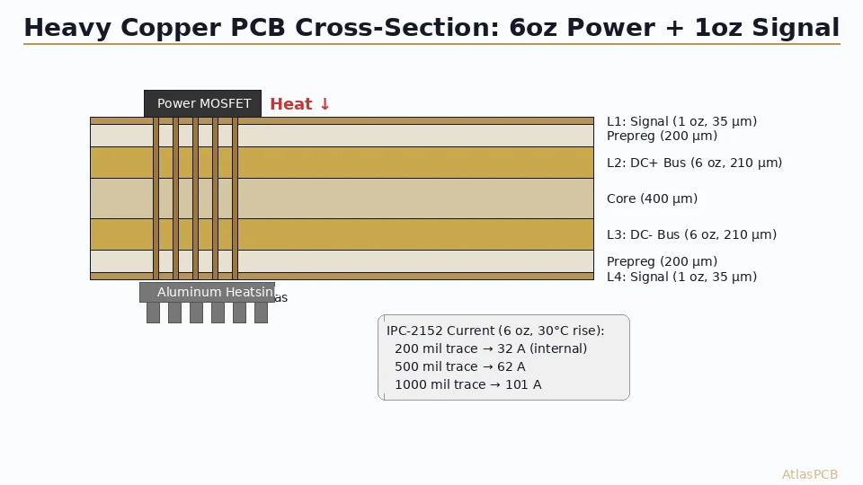
Typical Stack-up
Layer 1 (Top):     2oz  — Signal + component pads
Layer 2 (Inner):   6oz  — Power plane (high current)
Layer 3 (Inner):   6oz  — Ground plane (return current + heat spreading)
Layer 4 (Inner):   1oz  — Signal routing
Layer 5 (Inner):   1oz  — Signal routing
Layer 6 (Inner):   6oz  — Power plane
Layer 7 (Inner):   6oz  — Ground plane
Layer 8 (Bottom):  2oz  — Signal + component pads
This 8-layer stackup provides:
- 4 heavy copper planes for power distribution and heat management
- 2 standard copper signal layers for fine-pitch routing
- 2 moderate copper outer layers balancing component soldering with current capacity
Lamination Considerations
Mixing copper weights creates lamination challenges:
Resin fill: Heavy copper traces are 4-10x taller than standard traces, requiring more resin to fill the gaps. Standard prepreg may not provide enough resin flow. Specify high-resin-content prepreg adjacent to heavy copper layers.
Thickness uniformity: Different copper weights on different layers create asymmetric stress during lamination. This can cause warping if not balanced correctly. The stackup should be copper-balanced around the center axis.
Registration: Heavy copper layers etch more aggressively, and the dimensional stability of panels with mixed copper can differ from standard construction. Discuss registration tolerances with your manufacturer.
Thermal Design with Heavy Copper
Heat Spreading Analysis
For a power semiconductor dissipating 5W mounted on a 10mm × 10mm pad:
| Construction | Temperature Rise (no airflow) |
|---|---|
| 1oz copper, 20mm² spread area | ~45°C |
| 3oz copper, 50mm² spread area | ~18°C |
| 6oz copper, 100mm² spread area | ~8°C |
| 6oz copper, 100mm² + thermal via array | ~5°C |
Heavy copper’s thermal benefit comes from both increased copper thickness (lower thermal resistance through the conductor) and the ability to spread heat over a larger area before the FR4 thermal resistance becomes dominant.
Coin Insertion
For extreme thermal demands (>10W per component), copper coin insertion is an alternative to or complement for heavy copper. A solid copper slug (coin) is press-fit or epoxied into a routed cavity in the PCB, providing a direct thermal path from the component to a heatsink.
Heavy copper and copper coins can be combined — heavy copper spreads heat across the board surface while coins provide concentrated thermal vias for hotspot components.
Specification Best Practices
What to Include in Your Fab Notes
HEAVY COPPER SPECIFICATION:
- Layer 2, 5: 6oz finished copper minimum
- All other layers: 1oz finished copper minimum
- Minimum trace/space on heavy copper layers: 15mil/15mil
- Via: 16mil finished hole, 28mil pad, 1mil min barrel plating
- Thermal relief on all plane connections: 12mil spoke width
- Soldermask: 1mil minimum over copper features
- IPC-6012 Class 2 [or Class 3 for high-reliability]
- Cross-section verification required on first article
Common Specification Mistakes
- Not specifying finished vs starting copper weight — causes 30-50% copper thickness discrepancy
- Using standard trace/space rules on heavy copper layers — results in opens and shorts
- Forgetting etch compensation in impedance calculations — the trapezoidal profile changes impedance
- Direct plane connections without thermal relief — creates unmanufacturable solder joints
- Ignoring laminate resin requirements — standard prepreg can’t fill heavy copper gaps
Applications
Power Supply and Converter Design
Switch-mode power supplies, DC-DC converters, and inverters are the most common heavy copper applications. Bus bars carrying 20-100A can be integrated directly into the PCB, eliminating external bus bars and improving reliability.
Motor Drive and Control
Motor controller boards often carry phase currents of 10-50A. Heavy copper enables compact designs where power FETs, gate drivers, and current sense resistors share a single PCB with integrated high-current routing.
EV and Automotive Power Electronics
Electric vehicle power electronics increasingly use heavy copper PCBs for battery management, DC-DC conversion, and inverter pre-driver stages. IPC Class 3 construction with heavy copper is becoming the standard specification.
Industrial and Telecom Power
-48V telecom power systems, solar inverter control boards, and UPS power stages commonly specify 4-6oz copper for reliability over 15-20 year service lives.
At Atlas PCB, our partner facilities handle copper weights from 3oz to 12oz with full IPC Class 3 capability, including cross-section verification on first articles.
Frequently Asked Questions
Can I mix heavy copper on outer layers with standard copper on inner layers?
Yes, and this is common. However, the more typical approach is the reverse — heavy copper on inner layers and standard copper on outer layers. Inner heavy copper layers handle power distribution while outer standard copper layers accommodate fine-pitch component footprints. Outer heavy copper is used when components require high current directly through surface pads (power connectors, bus bars) or when exposed copper heat sinks are needed.
How does heavy copper affect board thickness?
Significantly. Each ounce of copper adds approximately 1.4mil (35µm) of thickness per layer. A 6-layer board with 6oz copper on all layers adds approximately 50mil (1.3mm) of copper alone — compared to 8.4mil for the same board with 1oz copper. Total board thickness must account for this, and the additional copper weight (mass) may matter for portable or weight-sensitive applications.
What is the maximum copper weight available in PCB manufacturing?
Most capable heavy copper manufacturers support up to 20oz (700µm). Beyond 20oz, direct-bonded copper (DBC) substrates or machined copper bus bar PCB hybrids become more practical. The practical limit for conventional PCB processes is around 10-12oz for internal layers (due to lamination constraints) and 20oz for external layers. Only a small number of manufacturers worldwide reliably produce boards above 10oz.
Further Reading
[High-Speed PCB Design: Signal Integrity Essentials for Modern Electronics]/blog/high-speed-pcb-design/)
[PCB Solder Mask: Types, Colors, and Functions Explained]/blog/pcb-solder-mask-guide/)
[IPC Class 3 Requirements: The Complete Guide for Designers]/blog/ipc-class-3-requirements/)
[PCB Thermal Management: Heat Dissipation Techniques for Reliable Electronics]/blog/pcb-thermal-management/)
[PCB Grounding Techniques: Star, Split, and Solid Ground Plane Strategies]/blog/pcb-grounding-techniques/)
[HDI PCB Design Guide: Stackup Rules, Via Structures & DFM Checklist]/blog/hdi-pcb-design-guide/)
About AtlasPCB — We specialize in complex PCB manufacturing for HDI, RF, and high-reliability applications. Explore our heavy copper PCB manufacturing, or get an aluminum and metal-core PCB services . Every order includes free engineering review. Get your quote.
Reviewed by AtlasPCB Engineering Team — IPC-certified manufacturing specialists with 15+ years of production experience in HDI, RF, and high-reliability PCB fabrication. Content based on factory floor data and real customer design reviews.
- heavy copper
- pcb design
- thermal management
- power electronics
- high current