· AtlasPCB Engineering · Engineering · 4 min read
PCB Thermal Management: Heat Dissipation Techniques for Reliable Electronics
Master PCB thermal management — understand heat sources, thermal vias, copper pours, thermal relief pads, metal-core PCBs, and simulation techniques for effective heat dissipation.

Heat is the enemy of electronics reliability. Every 10°C increase in junction temperature roughly halves the expected lifespan of a semiconductor. Effective PCB thermal management is critical for product longevity and performance.
Heat Sources on PCBs
- Power semiconductors: MOSFETs, IGBTs, voltage regulators — often the largest heat generators
- Processors/FPGAs: High-frequency switching creates significant heat
- Power resistors: Sense resistors and load resistors in power circuits
- LEDs: 60-80% of electrical energy becomes heat
- Inductors/transformers: Core and copper losses generate heat
Thermal Paths in a PCB
Heat travels through three mechanisms:
- Conduction: Through copper traces, planes, vias, and the substrate (primary mechanism in PCBs)
- Convection: From board surface to surrounding air (natural or forced)
- Radiation: Infrared emission from hot surfaces (minor contributor in most cases)
Copper thermal conductivity: 385 W/m·K FR-4 thermal conductivity: 0.25-0.3 W/m·K (through-plane), ~0.8 W/m·K (in-plane)
The huge difference means heat spreads easily along copper layers but poorly through the substrate thickness.
Thermal Design Techniques
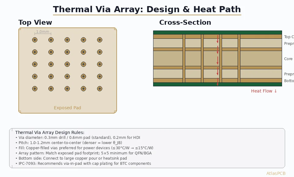
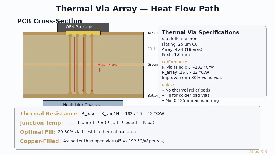
1. Thermal Vias
Plated vias under hot components transfer heat from the top layer to inner copper planes and the bottom layer.
Design guidelines:
- Via diameter: 0.3mm (12mil) typical
- Via pitch: 1.0-1.2mm grid
- Array size: Match the thermal pad of the component
- Copper fill recommended for better thermal performance (adds cost)
- Thermal conductivity of a via array: ~15-25 W/m·K (vs 0.25 for bare FR-4)
Example: A 5x5 array of 0.3mm vias on 1mm pitch under a QFN thermal pad reduces thermal resistance by approximately 60% compared to no vias.
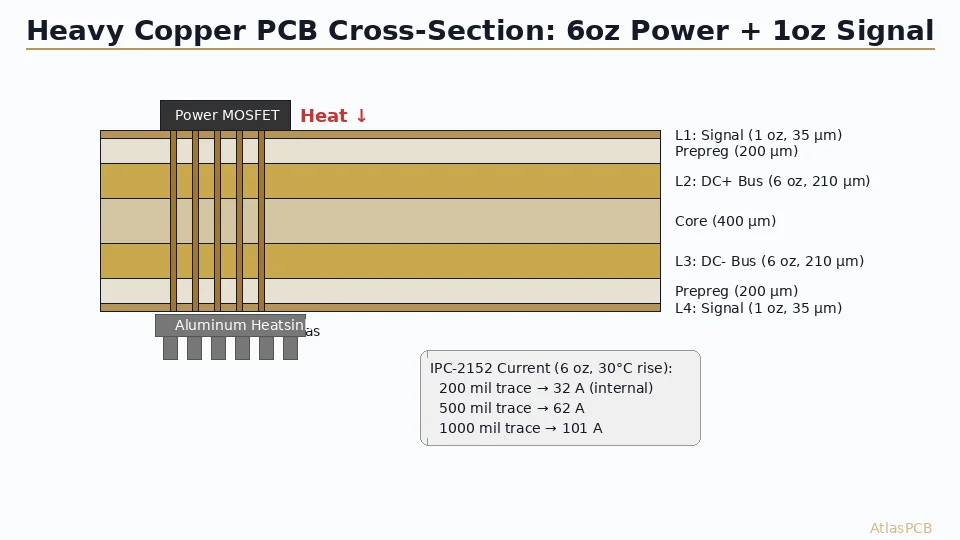
2. Copper Pours and Planes
Large copper areas act as heat spreaders.
- Use ground planes on inner layers for both electrical and thermal purposes
- Maximize copper fill on outer layers around heat-generating components
- Remove solder mask over thermal areas to improve convection (exposed copper pad)
- 2oz copper planes offer roughly double the heat spreading of 1oz
3. Thermal Relief Pads
When a component pad connects to a large copper plane, the plane acts as a heat sink during soldering, making it difficult to achieve proper solder flow.
Thermal relief patterns (spoke connections with 4 spokes, 8-10mil wide) limit heat flow during soldering while maintaining adequate thermal and electrical connection during operation.
When NOT to use thermal relief: On thermal pads of power components (QFN/QFP exposed pad) — these need maximum thermal conductivity. Use direct connection to plane.
4. Heatsink Attachment Areas
- Design flat copper areas for heatsink mounting
- Include mounting holes for clip or screw-on heatsinks
- Use thermal interface material (TIM) between component and heatsink
- Consider board-level heatsinks that bolt through the PCB
5. Component Placement Strategy
- Place hot components near board edges for better airflow
- Separate heat sources — don’t cluster hot components together
- Place temperature-sensitive components (crystals, references, sensors) away from heat sources
- Consider airflow direction in the enclosure when placing components

Metal Core PCBs (MCPCB)
For high-power applications where FR-4’s thermal performance is insufficient:
Structure
- Aluminum or copper base plate (1.0-3.0mm thick)
- Thin dielectric insulation layer (50-200um, thermal conductivity 1-8 W/m·K)
- Copper circuit layer (1-4oz)
Thermal Performance
| Board Type | Thermal Conductivity (through-plane) |
|---|---|
| Standard FR-4 | 0.25 W/m·K |
| FR-4 with thermal vias | 15-25 W/m·K |
| MCPCB (1 W/m·K dielectric) | ~1 W/m·K |
| MCPCB (3 W/m·K dielectric) | ~3 W/m·K |
| Direct copper bonded (DCB) | ~25 W/m·K |
Applications
- High-power LED lighting (street lights, automotive, industrial)
- Motor drivers
- Power supplies and DC-DC converters
- Automotive power electronics
Thermal Simulation
Before committing to fabrication, thermal simulation helps validate the design:
Tools
- ANSYS Icepak: Full 3D CFD simulation
- Mentor FloTHERM: Focused on electronics thermal analysis
- SimScale: Cloud-based thermal/CFD
- Free options: PCB thermal calculators, simplified spreadsheet models
What to Simulate
- Junction temperatures of critical components
- Board surface temperature distribution
- Airflow patterns in the enclosure
- Effect of heatsinks and thermal interfaces
- Copper plane heat spreading effectiveness
Thermal Measurement and Verification
IR Thermography
- Non-contact measurement of surface temperatures
- Provides a full thermal image of the board
- Useful for identifying hot spots and verifying simulation results
Thermocouples
- Point measurements at specific locations
- Higher accuracy than IR for specific component temperatures
- Can be used inside enclosures during thermal testing
Thermal Test Standards
- JEDEC JESD51: Standard for thermal characterization of semiconductor packages
- IPC-2152: Standard for determining current-carrying capacity (considers thermal effects)
Quick Design Checklist
- Identify components with highest power dissipation
- Calculate thermal resistance budget (junction to ambient)
- Add thermal vias under all exposed thermal pads
- Maximize copper area around hot components
- Consider 2oz copper for power layers
- Evaluate need for metal core or IMS substrate
- Plan airflow and heatsink attachment
- Simulate before fabrication
- Verify with IR thermography on first prototypes
Conclusion
Effective thermal management starts at the schematic/layout stage, not as an afterthought. By combining thermal vias, copper pours, proper component placement, and appropriate substrate materials, you can keep junction temperatures within safe limits and ensure long product life. For high-power applications, consider MCPCB technology or direct copper bonding for optimal thermal performance.
Further Reading
[PCB Solder Mask: Types, Colors, and Functions Explained]/blog/pcb-solder-mask-guide/)
[IPC Class 3 Requirements: The Complete Guide for Designers]/blog/ipc-class-3-requirements/)
About AtlasPCB — We specialize in complex PCB manufacturing for HDI, RF, and high-reliability applications. Explore our aluminum and metal-core PCB services . Every order includes free engineering review. Get your quote.
Reviewed by AtlasPCB Engineering Team — IPC-certified manufacturing specialists with 15+ years of production experience in HDI, RF, and high-reliability PCB fabrication. Content based on factory floor data and real customer design reviews.
- thermal management
- heat dissipation
- thermal via
- pcb design