· AtlasPCB Engineering · Engineering · 5 min read
PCB Design Rules: Trace Width, Spacing, and Via Size Guidelines
Master the essential PCB design rules — trace width for current capacity, minimum spacing for voltage isolation, via sizing standards, and design for manufacturability (DFM) best practices.

Proper PCB design rules ensure your board is manufacturable, reliable, and performs as intended. This guide covers the three most critical design parameters: trace width, trace spacing, and via sizing.
Trace Width: Current Carrying Capacity
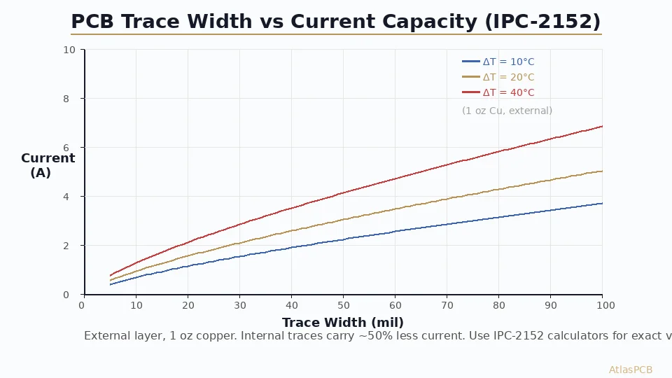
The width of a copper trace determines how much current it can safely carry without excessive temperature rise. The governing standard is IPC-2221 (Generic Standard on Printed Board Design).
IPC-2221 Trace Width Formula
The relationship between trace width, current, and temperature rise:
I = k x dT^0.44 x A^0.725
Where:
- I = current (Amps)
- k = 0.048 for outer layers, 0.024 for inner layers
- dT = temperature rise above ambient (degrees C)
- A = cross-sectional area of the trace (mils^2)
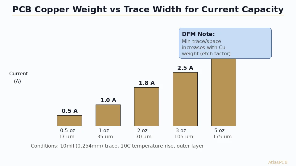
Quick Reference: Trace Width vs Current (1oz copper, 10C rise)
| Current (A) | External Layer Width | Internal Layer Width |
|---|---|---|
| 0.5 | 5 mil (0.13mm) | 10 mil (0.25mm) |
| 1.0 | 10 mil (0.25mm) | 20 mil (0.5mm) |
| 2.0 | 25 mil (0.63mm) | 50 mil (1.27mm) |
| 3.0 | 50 mil (1.27mm) | 100 mil (2.54mm) |
| 5.0 | 110 mil (2.8mm) | 220 mil (5.6mm) |
| 10.0 | 400 mil (10.2mm) | 800 mil (20.3mm) |
Key Notes:
- Internal layers dissipate heat less effectively — they need wider traces for the same current
- Doubling the copper weight (1oz to 2oz) roughly halves the required trace width
- Always add a safety margin of 20-50% above calculated minimums
Practical Guidelines
- Signal traces: 4-6 mil (0.1-0.15mm) for standard digital signals
- Power traces: Calculate based on maximum current + safety margin
- High-current (>5A): Consider copper pours/polygons instead of traces
- Thermal relief: Use spoke patterns on power plane connections to aid soldering
Trace Spacing: Voltage Isolation
Minimum trace spacing prevents arcing and ensures electrical isolation between nets at different voltages. Spacing requirements depend on the voltage difference and operating conditions.
IPC-2221B Spacing Requirements
| Voltage (DC or AC peak) | Internal Layers | External Layers (uncoated) | External (with conformal coating) |
|---|---|---|---|
| 0-15V | 2 mil (0.05mm) | 4 mil (0.1mm) | 2 mil (0.05mm) |
| 16-30V | 2 mil (0.05mm) | 4 mil (0.1mm) | 2 mil (0.05mm) |
| 31-50V | 4 mil (0.1mm) | 8 mil (0.2mm) | 2 mil (0.05mm) |
| 51-100V | 4 mil (0.1mm) | 8 mil (0.2mm) | 2 mil (0.05mm) |
| 101-150V | 8 mil (0.2mm) | 16 mil (0.4mm) | 4 mil (0.1mm) |
| 151-300V | 8 mil (0.2mm) | 32 mil (0.8mm) | 8 mil (0.2mm) |
| 301-500V | 16 mil (0.4mm) | 64 mil (1.6mm) | 16 mil (0.4mm) |
Safety Standard Requirements
For products requiring safety certification (UL, CE, IEC):
- IEC 60950/62368-1 (IT equipment): Requires creepage and clearance distances based on pollution degree, working voltage, and insulation type
- IEC 60601 (medical): More stringent requirements — 2x MOPP (Means of Patient Protection) typically requires 8mm creepage for mains isolation
- UL 60950: Similar to IEC 60950 with additional requirements for North America
Creepage vs Clearance:
- Clearance: Shortest distance through air between two conductors
- Creepage: Shortest distance along the surface of insulation between two conductors
- Creepage is always >= clearance due to surface contamination risk
Practical Guidelines
- Standard digital signals: 4-6 mil spacing (matches trace width)
- Mixed signal (analog + digital): 10-20 mil guard traces or spacing between domains
- High voltage (mains): Follow IEC/UL standards strictly; use slots/cutouts for reinforced insulation
- RF signals: Spacing affects impedance; use field solver for controlled impedance

Via Design
Vias are plated holes connecting traces between PCB layers. Proper via design ensures reliable inter-layer connections and manufacturable boards.
Via Types and Sizes
| Via Type | Drill Diameter | Pad Diameter | Aspect Ratio | Cost Impact |
|---|---|---|---|---|
| Standard through-hole | 0.3mm (12mil) | 0.6mm (24mil) | <8:1 | Baseline |
| Small through-hole | 0.2mm (8mil) | 0.45mm (18mil) | <10:1 | +10-20% |
| Microvia (laser) | 0.1mm (4mil) | 0.25mm (10mil) | <1:1 | +30-50% |
| Blind via | 0.15-0.3mm | 0.4-0.6mm | <1:1 | +20-40% |
| Buried via | 0.15-0.3mm | 0.4-0.6mm | <8:1 | +30-50% |
Via Design Rules
Annular Ring: The annular ring is the copper ring around the drilled hole. Minimum values:
- IPC Class 2: 5 mil (0.127mm)
- IPC Class 3: 7 mil (0.178mm)
- Recommended: 8-10 mil (0.2-0.25mm) for reliability
Formula: Annular ring = (Pad diameter - Drill diameter) / 2
Aspect Ratio: The ratio of board thickness to drill diameter. Higher ratios are harder to plate reliably.
- Standard capability: 8:1 (e.g., 1.6mm board / 0.2mm drill)
- Advanced capability: 10:1-12:1
- HDI microvia: <=1:1
Via Current Capacity: A 0.3mm plated via with 25um copper plating can carry approximately 1A continuous. For higher currents, use multiple vias in parallel.
Via-in-Pad
Placing vias directly in SMD pads (especially BGA) requires via fill and cap plating:
- Via is drilled and plated
- Via is filled with non-conductive epoxy or conductive paste
- Surface is planarized and cap-plated with copper
This adds cost but is essential for BGA breakout with fine-pitch packages (0.4-0.8mm pitch).
DFM (Design for Manufacturability) Best Practices
Minimum Feature Sizes (Standard Process)
| Feature | Minimum | Recommended |
|---|---|---|
| Trace width | 3 mil (0.075mm) | 4-5 mil (0.1-0.13mm) |
| Trace spacing | 3 mil (0.075mm) | 4-5 mil (0.1-0.13mm) |
| Drill size | 0.15mm | 0.2-0.3mm |
| Annular ring | 3 mil (0.075mm) | 5-8 mil (0.13-0.2mm) |
| Solder mask dam | 3 mil (0.075mm) | 4 mil (0.1mm) |
| Silkscreen width | 4 mil (0.1mm) | 5-6 mil (0.13-0.15mm) |
Common DFM Issues
- Acid traps: Acute angles (<90 degrees) in traces trap etchant and cause over-etching. Use 45-degree bends or arcs.
- Copper slivers: Very narrow copper features that can detach. Minimum copper feature width: 4 mil.
- Starved thermals: Thermal relief spokes too narrow for reliable plating. Minimum spoke width: 8 mil.
- Tombstoning risk: Unequal pad sizes or thermal imbalance on passive components. Ensure symmetric pad design and copper balance.
- Missing solder mask dams: Solder mask between adjacent pads prevents solder bridging. Minimum dam width: 3 mil.
Conclusion
Following proper PCB design rules from the start saves time, money, and manufacturing headaches. Always use your manufacturer’s specific design rules (available in their DFM guidelines) as they may differ from generic IPC recommendations. When in doubt, use larger features — the small cost of wider traces and bigger vias is far less than the cost of board respins due to manufacturing failures.
Further Reading
[HDI PCB Design Guide: Stackup Rules, Via Structures & DFM Checklist]/blog/hdi-pcb-design-guide/)
[HDI PCB Technology: Microvias, Laser Drilling, and High-Density Design]/blog/hdi-pcb-technology/)
[Via-in-Pad Design: Filled, Capped, and Plated Over — Complete Guide]/blog/via-in-pad-design/)
[Blind Via vs Buried Via: Design Rules, Cost Impact & When to Use Each]/blog/blind-via-vs-buried-via/)
[Controlled Impedance PCB: Design, Stackup & Testing Explained]/blog/controlled-impedance-pcb/)
[PCB DFM Checklist: 50 Points to Review Before Sending Gerbers]/blog/pcb-dfm-checklist/)
[PCB Solder Mask: Types, Colors, and Functions Explained]/blog/pcb-solder-mask-guide/)
[IPC Class 3 Requirements: The Complete Guide for Designers]/blog/ipc-class-3-requirements/)
About AtlasPCB — We specialize in complex PCB manufacturing for HDI, RF, and high-reliability applications. Explore our free engineering DFM review . Every order includes free engineering review. Get your quote.
Reviewed by AtlasPCB Engineering Team — IPC-certified manufacturing specialists with 15+ years of production experience in HDI, RF, and high-reliability PCB fabrication. Content based on factory floor data and real customer design reviews.
- pcb design
- trace width
- design rules
- DFM