· AtlasPCB Engineering · Engineering · 11 min read
Impedance Controlled PCB Manufacturer: ±5% Guaranteed with TDR Testing
How to choose a PCB manufacturer for controlled impedance boards. Covers TDR testing, stackup simulation, tolerance verification, and what separates ±5% guaranteed from ±10% nominal.
Every modern PCB with high-speed digital or RF signals requires controlled impedance traces. The question is not whether you need impedance control — it is whether your manufacturer can actually deliver it.
Many manufacturers advertise “controlled impedance capability.” Fewer can consistently achieve ±5% tolerance. This guide explains what controlled impedance manufacturing actually requires, how to evaluate a manufacturer’s capability, and what questions to ask.
What Controlled Impedance Means in Manufacturing
Controlled impedance means the manufacturer controls the physical parameters of your transmission lines — trace width, dielectric height, copper thickness, and dielectric constant — tightly enough to produce a predictable characteristic impedance.
The target impedance is determined by your design. Common targets:
| Application | Impedance Type | Target | Typical Tolerance |
|---|---|---|---|
| USB 2.0 | Differential | 90Ω | ±10% |
| USB 3.0/3.1 | Differential | 85Ω | ±10% |
| HDMI | Differential | 100Ω | ±10% |
| PCIe Gen 3/4/5 | Differential | 85Ω | ±10% |
| DDR4 | Single-ended | 40Ω | ±10% |
| DDR5 | Single-ended | 34Ω | ±10% |
| Ethernet 1G/10G | Differential | 100Ω | ±10% |
| 50Ω general RF | Single-ended | 50Ω | ±5% |
| 75Ω video/coax | Single-ended | 75Ω | ±5% |
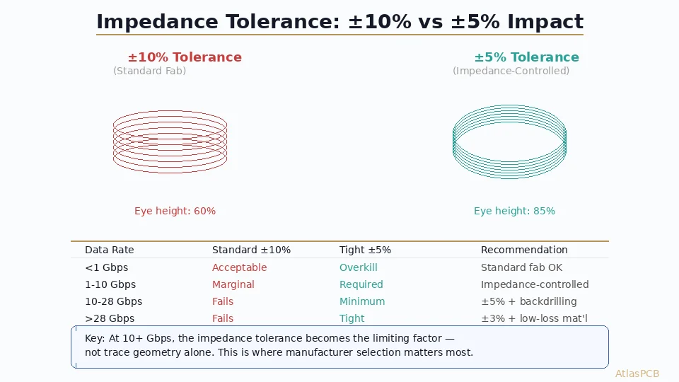
Note that most digital interface specs allow ±10%. RF applications typically demand ±5% or tighter. If your application requires ±5%, you need a manufacturer with proven capability — not one that simply quotes ±5% because you asked for it.
The Three Pillars of Impedance Control
Achieving and verifying controlled impedance requires three capabilities that work together:
Pillar 1: Pre-Production Stackup Simulation
Before manufacturing begins, the manufacturer must simulate impedance on your actual stackup using a validated field solver — not an online calculator.
What a field solver does that calculators do not:
- Accounts for trapezoidal trace cross-section (not rectangular — real traces have etched sidewalls)
- Models the actual glass weave pattern and resin content of the specific prepreg
- Handles differential pairs with asymmetric coupling
- Calculates impedance for embedded (stripline) and surface (microstrip) traces using frequency-dependent Dk
- Includes solder mask effect on surface traces (adds 1-3Ω to microstrip impedance)
Common field solvers: Polar SI, Simbeor, HyperLynx, Ansys HFSS (for critical applications).
What should happen: The manufacturer’s engineer runs your trace geometry through the field solver with the actual material properties (Dk, copper weight, dielectric height for the prepreg/core lot they will use). If the calculated impedance does not meet your target, they propose trace width adjustments before production.
Red flag: If the manufacturer says “we’ll use our standard stackup for your impedance” without simulating your specific trace widths and targets, they are not performing proper impedance engineering.
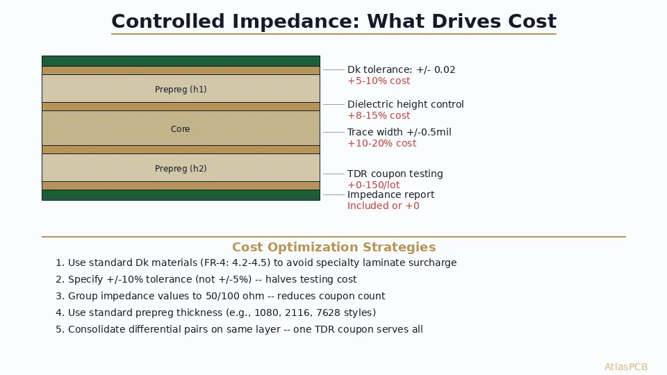
Pillar 2: Dielectric Thickness Control
Impedance is primarily determined by three variables: trace width, dielectric height (distance to reference plane), and dielectric constant. Of these, dielectric height has the largest manufacturing variation.
The physics: For a 50Ω microstrip on FR4 (Dk ≈ 4.2), every 0.5 mil change in dielectric height shifts impedance by approximately 1.5-2Ω. On a tight tolerance board, this is 3-4% of target — consuming most of your ±5% budget.
How dielectric thickness is controlled:
| Factor | Impact on Dk Thickness | Control Method |
|---|---|---|
| Prepreg resin content | ±0.3-0.5 mil | Incoming inspection, lot selection |
| Press pressure | ±0.2-0.3 mil | Calibrated press, vacuum assist |
| Copper pattern density | ±0.1-0.5 mil (resin flow into etch patterns) | Copper balance, fill patterns |
| Temperature profile | ±0.1-0.2 mil | Programmable press with thermocouple monitoring |
Commodity manufacturer approach: Use whatever prepreg is in stock, standard press recipe, no incoming inspection. Dielectric tolerance: ±1.0-1.5 mil.
Controlled impedance manufacturer approach: Incoming prepreg inspection (measure actual thickness), lot-specific Dk testing or certification, optimized press recipe per material type, copper balance review. Dielectric tolerance: ±0.5 mil.
The difference between ±1.0 mil and ±0.5 mil dielectric tolerance is the difference between ±10% and ±5% impedance tolerance.
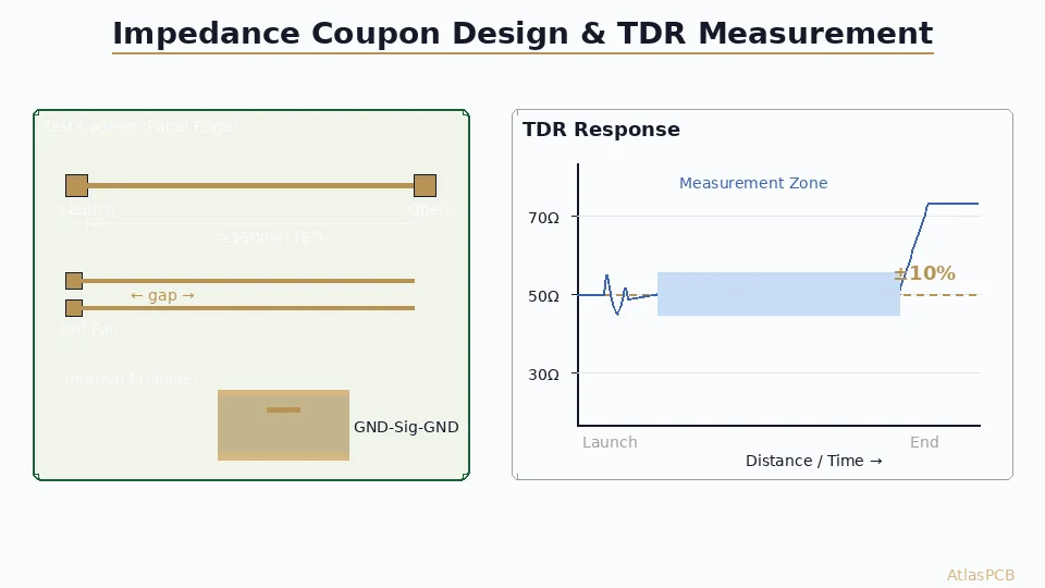
Pillar 3: TDR Verification
TDR (Time Domain Reflectometry) testing measures the actual impedance of manufactured traces. It is the only way to verify that the manufactured board meets its impedance specification.
How TDR works:
- A fast-edge pulse (typically 35ps rise time for PCB testing) is launched into the test coupon trace
- The TDR instrument measures the reflected signal as a function of time (which corresponds to distance along the trace)
- The impedance at each point is calculated from the reflection coefficient
- The measurement is compared to the target and tolerance
Impedance test coupons:
Every production panel includes impedance test coupons — dedicated trace structures designed specifically for TDR measurement. These coupons are fabricated on the same panel as your boards, using the same materials and processes.
A properly designed coupon set includes:
- At least one coupon per unique impedance requirement (e.g., one for 50Ω microstrip, one for 100Ω differential stripline)
- Coupons on both edges of the panel (to verify impedance uniformity across the panel)
- Launch pads compatible with the TDR probe
What you should receive: TDR measurement data showing measured impedance for each coupon, alongside the target value and tolerance. This data should accompany every shipment — not be available “on request.”

What Affects Impedance and How Much
Understanding impedance sensitivity helps you evaluate whether a manufacturer’s process controls are adequate.
| Variable | Typical Variation | Impedance Impact (50Ω microstrip) |
|---|---|---|
| Dielectric height ±0.5 mil | Common | ±1.5-2.0Ω (±3-4%) |
| Trace width ±0.5 mil | Common | ±1.0-1.5Ω (±2-3%) |
| Copper thickness ±0.2 mil | Common | ±0.3-0.5Ω (±0.5-1%) |
| Dk variation ±3% | FR4 typical | ±1.0-1.5Ω (±2-3%) |
| Dk variation ±1.5% | Rogers typical | ±0.5-0.8Ω (±1-1.5%) |
| Etch factor variation | Geometry-dependent | ±0.5-1.0Ω (±1-2%) |
| Solder mask presence | Microstrip only | +1-3Ω (systematic, can be modeled) |
Worst case: If all variations stack in the same direction, a 50Ω trace can shift by ±5-8Ω (±10-16%) with commodity process controls. This is why ±10% tolerance is achievable by almost anyone, and ±5% requires process discipline.
To achieve ±5%: The manufacturer must control dielectric thickness to ±0.5 mil, trace width to ±0.3 mil, and use validated Dk values — not generic datasheet numbers.
Common Impedance Failure Modes
Failure 1: Wrong Dk Value in Calculation
The manufacturer uses a generic Dk value (e.g., 4.2 for “FR4”) that does not match the actual material. Different FR4 grades range from 3.9 to 4.7 at 1GHz.
Result: Systematic impedance offset — all traces on all boards are high or low by the same amount.
Prevention: Manufacturer uses lot-specific Dk data or at minimum, the specific laminate grade’s published Dk at the relevant frequency.
Failure 2: Dielectric Thickness Drift
Press parameters are not optimized for the specific prepreg/core combination. Resin flow under pressure is excessive or insufficient.
Result: Impedance varies across the panel and between production lots.
Prevention: Press recipe validation per material combination, incoming prepreg thickness measurement, and post-press microsection verification on first articles.
Failure 3: Trace Width Over-Etch or Under-Etch
Etching removes copper to form traces. The etch rate depends on copper weight, etchant chemistry, conveyor speed, and spray pressure. Variations in any of these change the final trace width.
Result: Traces are narrower (higher impedance) or wider (lower impedance) than designed.
Prevention: Etch compensation in artwork generation (add width to compensate for expected etch), routine etch factor monitoring, and trace width measurement on test coupons.
Failure 4: No Solder Mask Compensation
Solder mask increases the effective dielectric constant for surface microstrip traces, adding 1-3Ω to measured impedance. If the field solver does not include solder mask, the pre-production impedance prediction is systematically low.
Result: Surface microstrip traces consistently measure 1-3Ω above the predicted value.
Prevention: Include solder mask in the impedance model. Most modern field solvers support this.
Failure 5: Coupon-to-Board Mismatch
Impedance coupons are at the panel edge where dielectric thickness, etch factor, and copper plating may differ from the center of the panel where your boards are located.
Result: Coupons pass TDR testing, but actual board traces are out of spec.
Prevention: Use coupons on both edges of the panel and include at least one coupon embedded within the production array. Compare coupon measurements to cross-section measurements from sacrificial boards periodically.
How to Evaluate an Impedance-Controlled PCB Manufacturer
Question 1: What field solver do you use?
Good answer: Names a specific tool (Polar SI, Simbeor, etc.) and can describe their validation process.
Weak answer: “We use our own calculator” or “We use the IPC formula.” IPC-2141 formulas are first-order approximations — adequate for rough estimation but not for ±5% production work.
Question 2: How do you determine the Dk value for impedance calculation?
Good answer: “We use the laminate manufacturer’s Dk data for the specific grade and frequency, validated against our TDR measurement history.”
Weak answer: “We use 4.2 for FR4.” This is a generic number that may be off by 5-10%.
Question 3: What dielectric thickness tolerance do you achieve?
Good answer: “±0.5 mil for standard prepreg, ±0.3 mil for controlled impedance builds.”
Weak answer: “We follow the prepreg manufacturer’s specification.” (This is typically ±10%, which means ±1-2 mil.)
Question 4: Do you provide TDR data with every shipment?
Good answer: “Yes, TDR impedance test data is included in the quality documentation for every controlled impedance order.”
Weak answer: “We can provide it if you request it.” (Means they do not routinely test.)
Question 5: What happens if impedance is out of spec?
Good answer: “We hold the lot, investigate root cause, and contact you with options — remake at our cost, accept with deviation, or adjusted trace width for rerun.”
Weak answer: “That rarely happens.” (Means they do not catch it when it does.)
Impedance Control at Different Layer Positions
Impedance control accuracy varies by layer position due to differences in dielectric thickness control:
| Layer Position | Trace Type | Typical Achievable Tolerance |
|---|---|---|
| Outer layer (L1/LN) | Microstrip | ±5-7% (solder mask adds variability) |
| Inner layer adjacent to outer | Embedded microstrip | ±5% (good dielectric control on single prepreg) |
| Inner layer — core | Stripline | ±5% (core thickness well-controlled) |
| Inner layer — between prepregs | Dual stripline | ±7% (two prepreg layers compound tolerance) |
Key insight: Stripline on a core is generally easier to control than microstrip, because core thickness is manufactured to tighter tolerances than pressed prepreg thickness. If you have flexibility in layer assignment, place your tightest impedance traces on stripline layers.
How Atlas PCB Handles Controlled Impedance
Controlled impedance is a core capability — not an add-on service. Every impedance-controlled order includes:
- Pre-production stackup simulation using Polar SI field solver with lot-specific material data
- Impedance-optimized trace width — if your specified geometry does not hit target, we propose adjustments before production
- TDR test data on production coupons with every shipment — not on request
- ±5% tolerance guarantee for single-ended traces, ±8% for differential pairs (±5% differential available for critical applications)
- Cross-section measurement available on request, included as standard for first articles
- Solder mask compensation included in microstrip impedance modeling
Every order includes a 12-hour engineering pre-audit. Impedance is verified on the actual stackup with actual materials before production begins. If your trace geometry needs adjustment, you know before — not after — the boards are made.
Frequently Asked Questions
What is TDR testing for PCBs?
TDR (Time Domain Reflectometry) sends a fast electrical pulse down a PCB trace and measures reflections to determine the characteristic impedance at every point along the trace. In PCB manufacturing, TDR is performed on impedance test coupons fabricated alongside the production panel — not on the actual product boards (which would require destructive probing). The measurement verifies that the manufactured dielectric thickness, trace width, and Dk combine to produce the target impedance within the specified tolerance. TDR accuracy is typically ±1-2Ω for a calibrated system.
What is the difference between ±5% and ±10% impedance tolerance?
For a 50Ω target: ±10% allows 45Ω to 55Ω; ±5% allows 47.5Ω to 52.5Ω. The halved tolerance window requires proportionally tighter process control — dielectric thickness held to ±0.5 mil instead of ±1 mil, trace width controlled to ±0.3 mil, and Dk values validated per material lot instead of assumed from datasheets. Most commodity manufacturers can hold ±10% without difficulty; ±5% requires active process monitoring and field solver-based impedance engineering. The cost difference is typically 5-15% for the tighter tolerance.
When do I need controlled impedance on my PCB?
You need controlled impedance when signal rise time is fast enough that traces behave as transmission lines. The practical threshold: signals above 100MHz frequency or with rise times under 1ns, on traces longer than approximately 25mm. This includes nearly all modern digital interfaces (USB, HDMI, PCIe, DDR, Ethernet) and all RF circuits. Single-ended 50Ω and differential 100Ω are the most common targets. Even if your interface specification allows ±10%, getting impedance right improves signal integrity margins and reduces EMI.
Summary
- Controlled impedance requires three capabilities: field solver simulation, dielectric thickness control, and TDR verification
- ±10% is commodity capability; ±5% requires disciplined process control and validated material data
- Dielectric height is the dominant variable — ±0.5 mil control is necessary for ±5% impedance tolerance
- TDR test data should accompany every impedance-controlled shipment as standard documentation
- Evaluate manufacturers on their field solver, Dk source data, dielectric tolerance, and TDR reporting practices
Need guaranteed impedance on your next board? Upload your Gerbers for a free engineering review — we simulate impedance on your actual stackup and verify with TDR on every production panel.
Related guides: [PCB Impedance Control]/blog/pcb-impedance-control/) | [PCB Stackup Design Guide]/blog/pcb-stackup-design-guide/) | [PCB Materials Guide]/blog/pcb-materials-guide/)
Further Reading
[Controlled Impedance PCB: Design, Stackup & Testing Explained]/blog/controlled-impedance-pcb/)
[Microstrip vs Stripline: Routing Strategies for Controlled Impedance PCBs]/blog/microstrip-vs-stripline/)
[High-Speed PCB Design: Signal Integrity Essentials for Modern Electronics]/blog/high-speed-pcb-design/)
[Multilayer PCB Stackup Design Guide: 8 to 30+ Layers Step by Step]/blog/multilayer-pcb-stackup-design-guide/)
[PCB Manufacturer with Engineering Review: Why Human DFM Audit Matters]/blog/pcb-manufacturer-engineering-review/)
[PCB DFM Checklist: 50 Points to Review Before Sending Gerbers]/blog/pcb-dfm-checklist/)
[PCB Solder Mask: Types, Colors, and Functions Explained]/blog/pcb-solder-mask-guide/)
[RF PCB Manufacturer: What to Look For in a High-Frequency Board Supplier]/blog/rf-pcb-manufacturer/)
[IPC Class 3 Requirements: The Complete Guide for Designers]/blog/ipc-class-3-requirements/)
[EMC/EMI Design for PCBs: Passing Compliance on the First Try]/blog/emc-emi-pcb-design/)
About AtlasPCB — We specialize in complex PCB manufacturing for HDI, RF, and high-reliability applications. Explore our impedance-controlled PCB manufacturing . Every order includes free engineering review. Get your quote.
Reviewed by AtlasPCB Engineering Team — IPC-certified manufacturing specialists with 15+ years of production experience in HDI, RF, and high-reliability PCB fabrication. Content based on factory floor data and real customer design reviews.
- impedance control
- TDR testing
- controlled impedance
- pcb manufacturer
- signal integrity