· AtlasPCB Engineering · Engineering · 11 min read
Multilayer FR4 PCB Manufacturer: 8 to 68 Layers with Precision Alignment
How to choose a multilayer FR4 PCB manufacturer for 8-68 layer boards. Covers sequential lamination, impedance control, registration tolerance, and supplier evaluation criteria.
Multilayer FR4 PCBs are the backbone of modern electronics — from telecom switching equipment and server backplanes to medical imaging systems and aerospace avionics. Once your design exceeds 8 layers, the choice of manufacturer stops being about price and starts being about capability.
This guide covers what separates a capable multilayer FR4 manufacturer from a commodity shop, what to verify before placing an order, and how to avoid the most expensive mistakes in high-layer-count board production.
Why High-Layer-Count FR4 Needs a Specialist
A 4-layer FR4 board is a commodity. Nearly any PCB manufacturer can produce one reliably. But as layer count increases, manufacturing complexity scales non-linearly.
Here is what changes above 8 layers:
- Sequential lamination replaces single-press construction. A 16-layer board may require 3-4 separate lamination cycles, each introducing registration error and thermal stress.
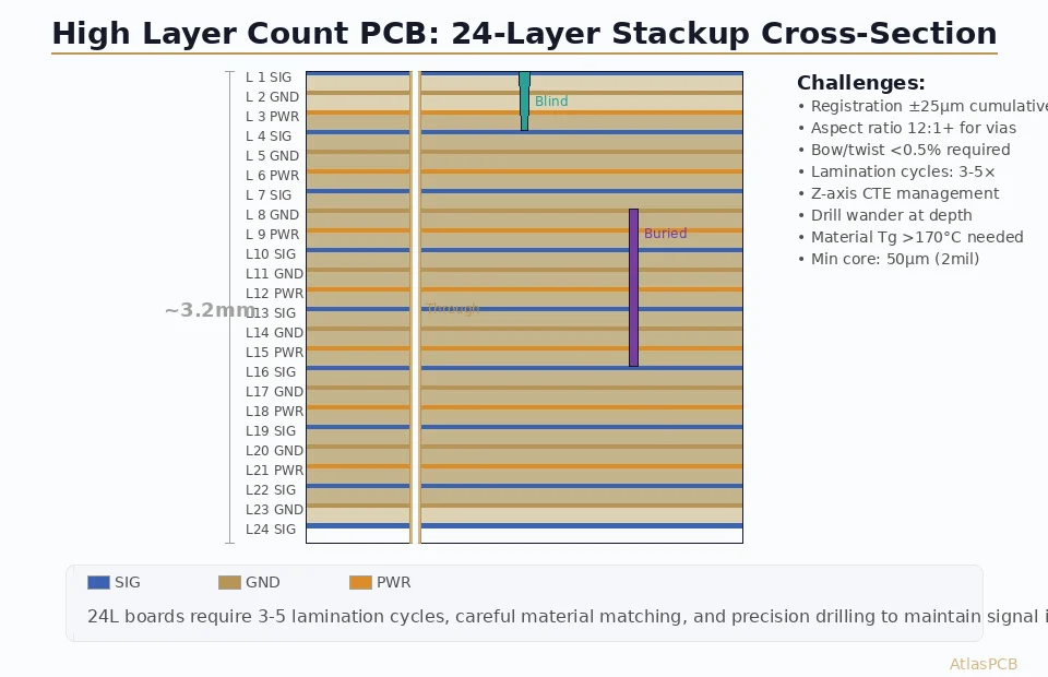
- Registration tolerance compounds with each press cycle. A ±1 mil error per cycle becomes ±3-4 mil total on a 24-layer board — enough to violate annular ring requirements on fine-pitch vias.
- Impedance control becomes harder as more reference planes compete for stackup real estate. Maintaining ±5% impedance across 16+ layers requires precise dielectric thickness control (±0.5 mil) and validated field solver models.
- Aspect ratio limits constrain via design. A 3.0mm thick 24-layer board with 0.25mm drill diameter hits an aspect ratio of 12:1 — beyond the capability of most commodity shops.
- Warpage and bow increase with board thickness and asymmetric copper distribution. IPC-6012 Class 3 allows only 0.75% bow and twist.
A manufacturer that handles 2-4 layer boards all day may technically accept your 16-layer order. The question is whether they have the equipment, process controls, and engineering expertise to deliver it reliably.
What to Verify Before Choosing a Manufacturer
1. Maximum Layer Count and Track Record
Ask for the maximum layer count the factory has produced in the last 12 months — not the number on their website from a one-time sample run. A manufacturer claiming 40+ layer capability but running 90% of production at 4-6 layers is a risk.
What to ask: “How many 16+ layer boards did you produce last quarter?” If they cannot answer with a specific number, they are not a volume multilayer shop.
2. Sequential Lamination Capability
Boards above 8 layers typically require sequential lamination — pressing inner layer pairs first, then building up additional layers in subsequent press cycles. This process demands:
- Hydraulic press with vacuum assist — eliminates air entrapment between layers
- Programmable temperature/pressure profiles — different resin systems (standard Tg, mid-Tg, high-Tg) require different cure cycles
- Pin-less registration systems (optical or X-ray) — pin-based registration introduces error at each lamination cycle
Red flag: If a manufacturer uses only pin registration for boards above 12 layers, expect registration problems.
3. Registration Accuracy
Layer-to-layer registration is the single most critical metric for high-layer-count boards. Poor registration causes:
- Annular ring violations (via breaks out of pad)
- Impedance drift (trace-to-reference-plane spacing changes)
- Short circuits between layers in dense routing areas
| Layer Count | Typical Registration | Best-in-Class |
|---|---|---|
| 4-8 layers | ±3 mil (75μm) | ±2 mil (50μm) |
| 10-16 layers | ±3 mil (75μm) | ±2 mil (50μm) |
| 18-24 layers | ±4 mil (100μm) | ±2.5 mil (63μm) |
| 26-40 layers | ±4 mil (100μm) | ±3 mil (75μm) |
| 40+ layers | ±5 mil (125μm) | ±3.5 mil (90μm) |
Ask for: X-ray registration measurement data from a recent production lot in your target layer count range.
4. Impedance Control and TDR Testing
Controlled impedance is standard on high-layer-count boards. The manufacturer should provide:
- Pre-production stackup simulation using a validated field solver (not a simple calculator)
- TDR (Time Domain Reflectometry) testing on impedance coupons fabricated alongside your production panel
- ±5% impedance tolerance for single-ended traces, ±8% for differential pairs (some applications demand tighter)
Impedance accuracy depends on dielectric thickness control. For a standard 50Ω microstrip on FR4 (Dk ≈ 4.2), a ±0.5 mil variation in dielectric height causes approximately ±3Ω impedance shift. On a 20-layer board with 10 impedance-controlled layers, this tolerance must be maintained across every dielectric layer.
For more detail on impedance design, see our [PCB impedance control guide]/blog/pcb-impedance-control/).
5. Material Options and Tg Rating
Not all FR4 is the same. High-layer-count boards generate significant heat during multiple lamination cycles, and the resin system must withstand repeated thermal excursions.
| Material Grade | Tg (°C) | Td (°C) | Best For |
|---|---|---|---|
| Standard FR4 | 130-140 | 300 | 4-8 layers, consumer electronics |
| Mid-Tg FR4 | 150-155 | 325 | 8-16 layers, industrial |
| High-Tg FR4 | 170-180 | 340 | 16+ layers, automotive, server |
| Ultra-High-Tg | 190-200 | 350 | 24+ layers, lead-free reflow |
For boards above 16 layers, high-Tg FR4 (Tg ≥ 170°C) is not optional — it is a requirement. Each sequential lamination cycle subjects inner layers to another full cure profile. Standard Tg material degrades under repeated thermal exposure, leading to delamination in the field.
Common laminates for high-layer-count FR4:
- Shengyi S1000-2 / S1000-2M (Tg 170°C, widely available)
- ITEQ IT-180A (Tg 175°C)
- Isola 370HR (Tg 180°C, halogen-free option)
- Panasonic Megtron 6 (for hybrid high-speed + high-layer applications)
6. Drill Capability and Aspect Ratio
High-layer-count boards are thick. A 20-layer board is typically 2.4-3.0mm thick; a 32-layer board can reach 4.5-5.0mm. This creates drilling challenges:
- Aspect ratio = board thickness ÷ drill diameter. Most manufacturers cap at 10:1 for through-holes.
- Drill accuracy degrades with depth. A 0.3mm drill through a 3.0mm board deflects more than through a 1.6mm board.
- Buried and blind vias require multiple drill cycles and precise depth control.
| Via Type | Typical Min Drill | Typical Aspect Ratio |
|---|---|---|
| Through-hole | 0.20mm (8mil) | 8:1 to 12:1 |
| Blind via | 0.10mm (4mil) laser | 1:1 to 1.2:1 |
| Buried via | 0.15mm (6mil) | Depends on sub-lamination thickness |
| Back-drilled via | 0.45mm (18mil) | N/A — controlled depth |
Back-drilling is common on 16+ layer boards for high-speed applications — removing the unused stub of a through-hole via to reduce signal reflections above 3GHz. Verify your manufacturer offers back-drill with ±8 mil depth accuracy.
7. Quality System and Certifications
For high-reliability applications (medical, automotive, defense, telecom), certifications matter:
- ISO 9001 — baseline quality management system
- IATF 16949 — automotive quality (covers process FMEA, PPAP, control plans)
- IPC-6012 Class 3 — highest acceptability standard (tighter annular ring, cleanliness, plating)
- UL listing — flammability rating (UL 94 V-0)
- AS9100 — aerospace (if applicable)
Do not accept “we follow IPC standards” without seeing the actual certification. An IPC Class 3 capable process requires specific equipment, training, and audit history.

Commodity vs. Specialist: What You Actually Get
| Capability | Commodity PCB Shop | Specialist (Atlas PCB) |
|---|---|---|
| Layer count range | 2-8 layers (primary), up to 16 (claimed) | 8-68 layers (production proven) |
| Registration | ±4-5 mil (pin-based) | ±2-3 mil (optical/X-ray) |
| Impedance tolerance | ±10% | ±5% with TDR verification |
| Engineering review | Automated DRC only | 12-hour human CAM engineer audit |
| Material options | Standard Tg FR4 only | Standard, mid-Tg, high-Tg, halogen-free |
| Min order quantity | 5-10 pieces | 1 piece |
| Stackup support | ”Use our standard stackup” | Custom stackup simulation + optimization |
| Back-drill | Not available | ±8 mil depth accuracy |
| Quality docs | Certificate of conformance | Impedance report + material cert + microsection |
The price difference between commodity and specialist is real — expect 2-4x for the same layer count. But the cost of a failed prototype run (re-spin, re-order, 3-4 weeks lost) typically exceeds the price premium of getting it right the first time.
Real-World Example: 24-Layer Telecom Backplane
The board: 24-layer FR4, 400mm × 280mm, 4.2mm thick, 14 impedance-controlled layers (50Ω single-ended, 100Ω differential), 0.2mm minimum drill, back-drilled vias for 10Gbps+ signals.
The problem: The engineer’s initial manufacturer quoted the job based on their standard process. First prototypes showed ±15% impedance variation on inner layers (spec was ±5%), three layers had registration failures visible in cross-section, and two back-drilled vias penetrated past the target layer.
The root causes:
- Standard Tg FR4 was used instead of high-Tg — dielectric thickness shifted during the third lamination press
- Pin registration — accumulated error across 5 sequential press cycles exceeded pad capture
- Back-drill depth controlled by time, not depth sensor — inconsistent results
The solution: The board was moved to a manufacturer with high-Tg Shengyi S1000-2M, optical registration (CCD-based), impedance-coupled stackup simulation, and laser-depth-controlled back-drill. First article passed all specs.
The lesson: The specialist manufacturer cost 2.8x more per board. The failed first run at the commodity shop cost 4 weeks and the full price of the original order — plus engineering time to diagnose the failures. Total cost was 5x what it would have been to start with the right manufacturer.
Stackup Design Considerations for High-Layer-Count FR4
Stackup design for 8+ layer boards requires balancing multiple constraints simultaneously:
- Impedance targets — trace width and dielectric height must produce target impedance
- Symmetry — asymmetric copper distribution causes warpage during reflow
- Signal-ground pairing — every signal layer should have an adjacent reference plane
- Power delivery — low-impedance power/ground plane pairs for decoupling
- Manufacturability — total thickness must stay within press capability; prepreg/core selection must match available materials
General stackup rules for multilayer FR4:
- Maintain board symmetry around the center axis (mirror copper weight and dielectric)
- Place high-speed signal layers adjacent to solid ground planes
- Avoid routing on external layers when possible (use them for components and short fan-out only)
- Keep power and ground planes as close together as possible (2-4 mil prepreg) for decoupling
- Use the same prepreg type between symmetrically paired layers
For a deeper dive into stackup planning, see our [multilayer PCB stackup design guide]/blog/pcb-stackup-design-guide/).
Design for Manufacturability: Common Mistakes
Mistake 1: Ignoring Aspect Ratio Limits
Designers frequently specify 0.2mm vias on a 3.0mm board (15:1 aspect ratio) — beyond most manufacturers’ reliable capability. Either increase the drill size, use blind/buried vias to reduce effective depth, or confirm the factory can reliably plate at that ratio.
Mistake 2: Asymmetric Copper Distribution
A stackup with 2oz copper on layers 1-4 and 0.5oz on layers 5-8 will warp. Always check that copper weight is balanced around the board center.
Mistake 3: Specifying Standard Tg for High-Layer Boards
“FR4” is not a material specification — it is a material family. Specifying “FR4” without a Tg rating leaves the manufacturer free to use the cheapest option. Always specify minimum Tg, Td, and ideally a specific laminate grade.
Mistake 4: No Stackup Review Before Ordering
Sending Gerbers without a verified stackup is the number one cause of impedance failures on multilayer boards. The manufacturer should simulate impedance on your actual stackup — not a generic template — before production begins.
Mistake 5: Back-Drill Depth Not Specified
If your design needs back-drilling, specify the target stub length (typically ≤10 mil) and reference layer in your fab notes. Do not assume the manufacturer will figure it out from the Gerbers alone.
How Atlas PCB Handles Multilayer FR4
Atlas PCB works exclusively with certified manufacturing partners whose primary business is high-complexity boards. For multilayer FR4 specifically:
- Layer count: 8 to 68 layers in production (not a theoretical maximum)
- Registration: ±2 mil using optical alignment and X-ray verification
- Impedance: ±5% with TDR-verified impedance coupons on every production panel
- Materials: Shengyi S1000-2M, ITEQ IT-180A, Isola 370HR in standard stock; other laminates sourced on request
- Back-drill: Depth-controlled back-drilling with ±8 mil accuracy
- Minimum order: 1 piece. Prototypes receive the same engineering review as production runs.
Every order includes a 12-hour human engineering pre-audit. A CAM engineer reviews your stackup feasibility, impedance consistency, via structure risks, and DFM issues before production starts. If something does not work, we contact you directly — no silent modifications.
Frequently Asked Questions
How many layers can a multilayer FR4 PCB have?
Standard multilayer FR4 PCBs range from 4 to 68 layers. Boards with 8+ layers typically require sequential lamination, and boards above 20 layers demand specialized press equipment, precise registration systems, and careful thermal management during lamination. The practical limit depends on board size, total thickness constraints, and via architecture.
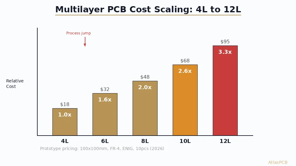
What is the cost difference between a 4-layer and 16-layer FR4 PCB?
A 16-layer FR4 board typically costs 5-8x more than an equivalent 4-layer board. The cost increase is non-linear because each additional lamination cycle adds press time, registration risk, and material handling steps. Additional cost drivers include tighter registration requirements, longer drill times for buried and blind vias, impedance verification, and higher material waste rates during sequential lamination.
What registration tolerance should I expect for high-layer-count PCBs?
Capable manufacturers achieve ±2 mil (50μm) layer-to-layer registration for boards up to 20 layers, and ±3 mil (75μm) for 30+ layer boards. Registration is the most critical quality metric for multilayer boards — it affects impedance accuracy, via-to-pad alignment, and annular ring compliance. For your first order with any manufacturer, request X-ray registration verification data to confirm their actual capability.
Summary
- Multilayer FR4 above 8 layers requires sequential lamination, optical registration, and high-Tg materials
- Registration tolerance, impedance control, and aspect ratio are the three metrics that separate capable manufacturers from commodity shops
- Always specify material grade (not just “FR4”), impedance requirements, and back-drill targets in your fab notes
- Request TDR impedance data, cross-section photos, and registration measurements from your manufacturer
- The cost of a failed prototype run almost always exceeds the price premium of a specialist manufacturer
Ready to get your multilayer FR4 board manufactured right? Upload your Gerbers for a free engineering review, or talk to an engineer about your specific stackup requirements.
Related guides: [PCB Stackup Design Guide]/blog/pcb-stackup-design-guide/) | [PCB Impedance Control]/blog/pcb-impedance-control/) | [HDI PCB Technology]/blog/hdi-pcb-technology/)
Further Reading
[HDI PCB Design Guide: Stackup Rules, Via Structures & DFM Checklist]/blog/hdi-pcb-design-guide/)
[PCB Sequential Lamination: Process, Design Rules, and When You Need It]/blog/pcb-sequential-lamination/)
[Blind Via vs Buried Via: Design Rules, Cost Impact & When to Use Each]/blog/blind-via-vs-buried-via/)
[Controlled Impedance PCB: Design, Stackup & Testing Explained]/blog/controlled-impedance-pcb/)
[Impedance Controlled PCB Manufacturer: ±5% Guaranteed with TDR Testing]/blog/impedance-controlled-pcb-manufacturer/)
[High-Multilayer FR4 vs Standard FR4: When to Upgrade Material Grade]/blog/high-multilayer-fr4-vs-standard-fr4/)
[Multilayer PCB Stackup Design Guide: 8 to 30+ Layers Step by Step]/blog/multilayer-pcb-stackup-design-guide/)
[PCB DFM Checklist: 50 Points to Review Before Sending Gerbers]/blog/pcb-dfm-checklist/)
[PCB Manufacturer with Engineering Review: Why Human DFM Audit Matters]/blog/pcb-manufacturer-engineering-review/)
[IPC Class 3 Requirements: The Complete Guide for Designers]/blog/ipc-class-3-requirements/)
About AtlasPCB — We specialize in complex PCB manufacturing for HDI, RF, and high-reliability applications. Explore our HDI PCB manufacturing capabilities, or get an multilayer PCB fabrication up to 30 layers . Every order includes free engineering review. Get your quote.
Reviewed by AtlasPCB Engineering Team — IPC-certified manufacturing specialists with 15+ years of production experience in HDI, RF, and high-reliability PCB fabrication. Content based on factory floor data and real customer design reviews.
- multilayer pcb
- fr4
- high layer count
- pcb manufacturer
- sequential lamination