· AtlasPCB Engineering · Engineering · 6 min read
PCB Fabrication Tolerances: Engineering Spec Guide
Complete reference for PCB fabrication tolerances — drill, trace width, registration, impedance, and board thickness specifications.
Why Fabrication Tolerances Matter
Every dimension on a PCB drawing — trace width, hole diameter, board thickness, copper weight — has an associated manufacturing tolerance. The nominal value is what you design to; the tolerance is how far the actual board can deviate from that nominal. Understanding these tolerances is essential for three reasons:
- Design margin: Your design must function across the entire tolerance range, not just at nominal values
- Cost optimization: Specifying tighter tolerances than necessary increases cost, lead time, and yield loss
- Supplier communication: Ambiguous tolerance callouts lead to manufacturing questions, delays, and potential quality issues
This guide provides the definitive reference for PCB fabrication tolerances across all major parameters, based on IPC standards and real-world manufacturing capabilities.
Drill Tolerances
Drilling is one of the most critical PCB manufacturing steps, and drill tolerances directly affect via reliability, component fit, and annular ring integrity.
Mechanical Drilling
| Parameter | Standard | Advanced | IPC Class 3 |
|---|---|---|---|
| Hole diameter | ±0.05 mm | ±0.03 mm | ±0.025 mm |
| Hole position | ±0.075 mm | ±0.05 mm | ±0.05 mm |
| Hole wall roughness | ≤25 µm | ≤15 µm | ≤15 µm |
| Min. drill diameter | 0.15 mm | 0.10 mm | 0.15 mm |
| Aspect ratio limit | 10:1 | 12:1 | 10:1 |
| Drill registration to features | ±0.075 mm | ±0.05 mm | ±0.05 mm |
Drill accuracy degrades with increasing aspect ratio. For boards thicker than 3.0 mm, expect wider position tolerances due to drill wander. [PCB aspect ratio and via design]/blog/pcb-aspect-ratio-via-design/) provides detailed guidance on managing these constraints.
Laser Drilling (Microvias)
| Parameter | Standard | Advanced |
|---|---|---|
| Via diameter | ±0.025 mm | ±0.015 mm |
| Via position | ±0.025 mm | ±0.015 mm |
| Depth control (blind vias) | ±15 µm | ±10 µm |
| Min. capture pad | Via dia. + 100 µm | Via dia. + 75 µm |
| Min. via diameter | 75 µm | 50 µm |
Laser drilling achieves significantly tighter tolerances than mechanical drilling, which is one reason [HDI PCB designs]/blog/hdi-pcb-technology/) use laser-drilled microvias for high-density areas.
Controlled-Depth Drilling (Back-Drill)
| Parameter | Standard | Advanced |
|---|---|---|
| Depth accuracy | ±0.15 mm | ±0.10 mm |
| Minimum remaining stub | 0.20 mm | 0.15 mm |
| Diameter tolerance | ±0.05 mm | ±0.03 mm |
Back-drill depth control is one of the more challenging tolerances. The stub length left after back-drilling directly affects signal integrity at high frequencies. For designs requiring back-drill, specify the maximum acceptable stub length rather than a specific drill depth — this gives the fabricator more process flexibility.
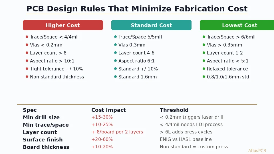
Trace Width and Spacing Tolerances
Trace width and spacing tolerances are primarily determined by the etching process and the starting copper weight.
Subtractive Etching
| Copper Weight | Nominal Trace Width | Width Tolerance | Min. Space |
|---|---|---|---|
| 1/3 oz (12 µm) | ≥75 µm | ±15% | 60 µm |
| 1/2 oz (18 µm) | ≥75 µm | ±18% | 75 µm |
| 1 oz (35 µm) | ≥100 µm | ±20% | 100 µm |
| 2 oz (70 µm) | ≥150 µm | ±25% | 150 µm |
| 3 oz (105 µm) | ≥200 µm | ±25% | 200 µm |
Thicker copper produces wider etch undercut, making trace width control more challenging. If your design requires tight trace width control with heavy copper, discuss process options with your fabricator.
Advanced Processes (mSAP, SAP)
| Process | Min. Trace Width | Width Tolerance |
|---|---|---|
| LDI + fine-line etch | 50 µm | ±15% |
| mSAP | 25 µm | ±10% |
| SAP (IC substrate) | 10 µm | ±8% |
Semi-additive processes achieve tighter tolerances because copper is plated up to the desired thickness rather than etched down. For critical [trace width and spacing designs]/blog/pcb-design-rules-trace-width-spacing/), understanding which process your fabricator uses is essential.
Layer Registration Tolerances
Layer-to-layer registration affects pad-to-drill alignment, impedance consistency, and minimum annular ring.
| Registration Type | Standard | Advanced | IPC Class 3 |
|---|---|---|---|
| Inner layer to inner layer | ±50 µm | ±35 µm | ±50 µm |
| Outer layer to inner layer | ±75 µm | ±50 µm | ±75 µm |
| Outer layer to drill | ±75 µm | ±50 µm | ±50 µm |
| Inner layer to drill | ±75 µm | ±50 µm | ±50 µm |
Registration accuracy is cumulative — a pad on an outer layer connecting to a drill that must align with an inner layer pad involves three tolerance stacks. This is why [annular ring design]/blog/pcb-annular-ring-ipc-standards/) must account for the combined registration tolerance of all involved layers.
Factors Affecting Registration
- Material CTE: Higher CTE laminates expand more during lamination, degrading registration
- Layer count: More layers mean more lamination cycles and cumulative registration error
- Board size: Larger panels have worse registration at the edges
- Lamination pressure and temperature: Process uniformity directly affects registration
Impedance Tolerances
Controlled impedance is critical for [signal integrity]/blog/signal-integrity-pcb-design-guide/) in high-speed designs. Impedance tolerance depends on how well the fabricator can control the variables that determine impedance: trace width, dielectric thickness, dielectric constant, and copper thickness.
| Tolerance Level | Cost Impact | Typical Application |
|---|---|---|
| ±10% | Standard pricing | Most digital designs |
| ±7% | +10-15% | High-speed SerDes, DDR4/5 |
| ±5% | +15-30% | RF, precision timing, DDR5 |
| ±3% | +40-60%+ | Specialized RF, test equipment |
Achieving tight impedance tolerance requires:
- Tighter [trace width tolerance]/blog/how-to-specify-impedance-pcb/) (the dominant variable)
- Thinner prepreg thickness tolerance (±5% rather than ±10%)
- Consistent Dk across the panel (material lot control)
- In-process impedance monitoring (not just final test coupons)
Board Thickness Tolerances
| Board Type | Nominal Range | Tolerance |
|---|---|---|
| Standard rigid | 0.4–3.2 mm | ±10% |
| Thin boards | 0.2–0.4 mm | ±15% |
| Thick boards | 3.2–6.0 mm | ±10% |
| Flex circuits | 0.05–0.5 mm | ±10% |
| Rigid-flex | Per section | ±10% rigid, ±15% flex |
Board thickness tolerance is a stackup tolerance — it reflects the cumulative variation in prepreg flow, copper thickness, and lamination pressure across all layers. For designs where board thickness is critical (connector mating, card-edge contacts, mechanical fit), specify the finished thickness tolerance explicitly and verify it with your fabricator.
Solder Mask Tolerances
| Parameter | Standard | Advanced |
|---|---|---|
| Registration to pads | ±75 µm | ±50 µm |
| Minimum dam (between pads) | 75 µm | 50 µm |
| Minimum web width | 100 µm | 75 µm |
| Thickness (over conductor) | 10–35 µm | 15–25 µm |
| Thickness (over laminate) | 15–50 µm | 20–35 µm |
Solder mask registration is particularly critical for fine-pitch components. For [BGA and QFN pad designs]/blog/pcb-pad-design-bga-qfn/) with pitch below 0.5 mm, verify that your fabricator’s solder mask process can achieve the required registration and minimum dam width.
Surface Finish Tolerances
| Finish | Parameter | Specification |
|---|---|---|
| HASL | Thickness | 1–40 µm (variable) |
| ENIG | Ni thickness | 3–6 µm (±1 µm) |
| ENIG | Au thickness | 0.05–0.10 µm (±0.02 µm) |
| OSP | Thickness | 0.2–0.5 µm |
| Immersion Ag | Thickness | 0.15–0.40 µm |
| Hard Gold | Thickness | 0.5–2.5 µm (±20%) |
Surface finish thickness affects solderability, contact resistance, and shelf life. For detailed comparison, see our [PCB surface finish guide]/blog/pcb-surface-finish-guide/).
How to Specify Tolerances on Your Drawing
Best practices for tolerance specification:
- Use IPC-6012 as the baseline: Specify “Fabrication per IPC-6012, Class X” to establish default tolerances
- Call out exceptions: Only specify tighter tolerances where your design actually requires them
- Provide tolerance rationale: Note why critical tolerances are required — this helps the fabricator prioritize
- Include a fabrication drawing: Don’t rely solely on Gerber notes — a dimensioned drawing prevents ambiguity
- Specify impedance in a table: List each impedance class with target, tolerance, layer, and trace width
Common Tolerance Specification Mistakes
- Over-specifying: Calling out ±5% impedance when ±10% would work fine
- Under-specifying: Not calling out critical tolerances and relying on fabricator defaults
- Conflicting callouts: Specifying a trace width that cannot achieve the specified impedance with available materials
- Missing stack-up: Providing impedance targets without a defined stackup
Design for Manufacturing Tolerance
The best approach to fabrication tolerances is to design with them in mind from the start:
- Size pads for worst-case registration: Account for drill position tolerance + layer registration tolerance when calculating [minimum annular ring]/blog/pcb-annular-ring-ipc-standards/)
- Route traces wider than minimum: Use 125% of minimum trace width where space allows
- Build in copper balance: Even copper distribution reduces [warpage]/blog/pcb-warpage-control-multilayer/) and improves thickness uniformity
- Verify your design at tolerance extremes: Run impedance simulations at minimum and maximum trace width/dielectric thickness
Atlas PCB Fabrication Capabilities
Atlas PCB’s standard manufacturing capabilities meet or exceed the “Advanced” tolerances listed in this guide. Every order includes a 12-hour engineering pre-audit where we verify that your design is within our process capabilities and flag any potential tolerance concerns before production begins.
Ready to get your design manufactured with precision? Upload your Gerbers for a free engineering review and our team will verify all critical tolerances against your design requirements.
Related guides: [PCB Design Rules: Trace Width & Spacing]/blog/pcb-design-rules-trace-width-spacing/) | [PCB Annular Ring & IPC Standards]/blog/pcb-annular-ring-ipc-standards/) | [How to Specify Impedance on PCB]/blog/how-to-specify-impedance-pcb/)
Further Reading
- [PCB Manufacturer with Engineering Review: Why Human DFM Audit Matters]/blog/pcb-manufacturer-engineering-review/)
- [PCB Panelization and Array Design: V-Score vs Tab Routing, DFM Rules, and Cost Optimization]/blog/pcb-panelization-v-score-tab-routing-dfm-cost-optimization/)
- [Rogers PCB Fabrication: Material Sourcing, Lead Times & Quality Control]/blog/rogers-pcb-fabrication/)
- [ENEPIG vs ENIG: Which PCB Surface Finish for Your Design?]/blog/enepig-vs-enig/)
- [PCB Surface Finish Selection — ENIG vs HASL vs OSP vs Hard Gold vs ENEPIG]/blog/pcb-surface-finish-enig-hasl-osp-hard-gold-enepig/)
- Get a Free DFM Review
About AtlasPCB — We specialize in complex PCB manufacturing for HDI, RF, and high-reliability applications. Explore our full PCB manufacturing capabilities, or get an instant online quote . Every order includes free engineering review. Get your quote.
Reviewed by AtlasPCB Engineering Team — IPC-certified manufacturing specialists with 15+ years of production experience in HDI, RF, and high-reliability PCB fabrication. Content based on factory floor data and real customer design reviews.
- fabrication-tolerance
- manufacturing-specs
- drill-accuracy
- trace-tolerance
- pcb-engineering