· AtlasPCB Engineering · Engineering · 12 min read
PCB Annular Ring: Minimum Width Requirements per IPC Standards
Complete guide to PCB annular ring requirements including IPC-6012 Class 2 and Class 3 minimums, breakout rules, drill tolerance compensation, and design tips for laser-drilled vs mechanical vias.
PCB Annular Ring: Minimum Width Requirements per IPC Standards
The annular ring — that thin ring of copper surrounding every drilled hole on a PCB — may seem like a minor geometric detail. But in practice, it is one of the most common causes of DFM violations, fabrication rejects, and reliability failures. An annular ring that’s too small leads to broken connections. One that’s too large wastes routing space. Getting it right requires understanding IPC requirements, manufacturing tolerances, and the interplay between drill accuracy and layer registration.
This article provides a complete reference for PCB annular ring design: what the IPC standards require, how to calculate the right pad size, the differences between mechanical and laser-drilled holes, and practical tips for avoiding common mistakes.
What Is an Annular Ring?
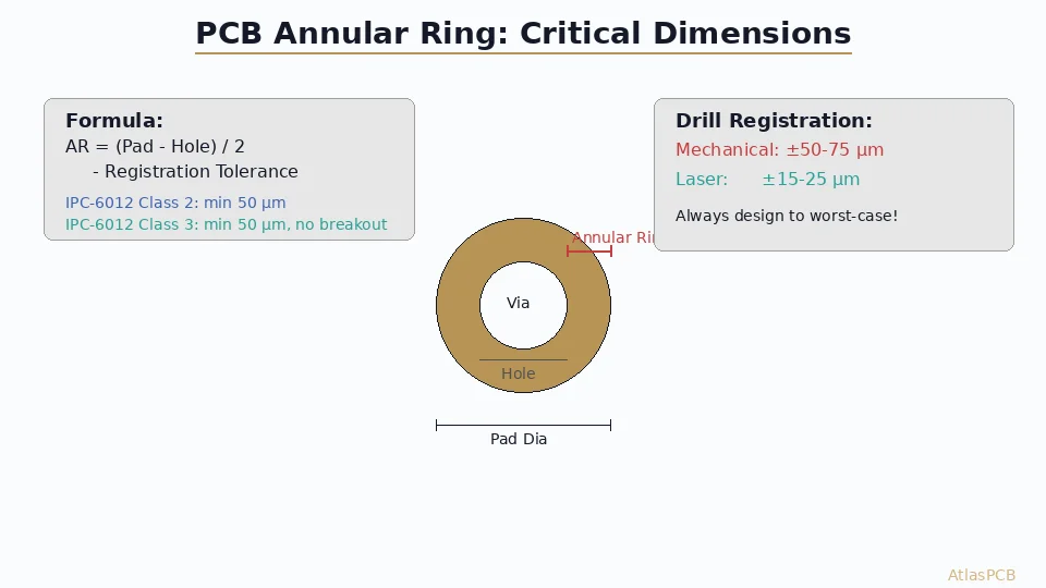
The annular ring is the width of copper pad remaining around a plated hole after drilling. It is measured as the shortest distance from the edge of the drilled hole to the edge of the pad.
Annular Ring Width = (Pad Diameter − Drilled Hole Diameter) ÷ 2
This is the nominal annular ring — the value you see in your CAD tool assuming perfect alignment. The actual annular ring on a manufactured board will be smaller on one side and larger on the other due to drill wander and layer misregistration.
Why Annular Ring Matters
The annular ring serves several critical functions:
- Electrical connection: It ensures the plated via barrel makes continuous contact with the pad copper on each layer
- Mechanical strength: A wider annular ring provides more copper for solder fillet formation and resists pad lifting during rework
- Thermal conduction: The ring provides a thermal path between the via and the surrounding copper
- Plating anchor: During electroplating, the annular ring provides the seed layer that allows copper to build up in the via barrel
When the drill breaks out beyond the pad boundary, the via barrel loses its connection to the pad on that layer. This is called breakout, and its acceptability depends on the IPC classification of the board.
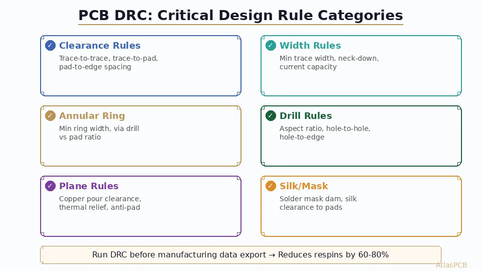
IPC-6012 Annular Ring Requirements
IPC-6012 (Qualification and Performance Specification for Rigid Printed Boards) is the governing standard for annular ring acceptance criteria. The requirements differ significantly between the three performance classes, as explained in our [IPC standards and PCB classes guide]/blog/ipc-standards-pcb-classes/).
Class 1 — General Electronic Products
- External layers: Minimum 50 µm (2 mil) annular ring; 90° breakout permitted
- Internal layers: 90° breakout permitted
- Application: Consumer electronics, disposable devices
- Interpretation: Very forgiving — essentially allows partial loss of the annular ring
Class 2 — Dedicated Service Electronic Products
- External layers: Minimum 50 µm (2 mil) annular ring at all points
- Internal layers: 90° breakout permitted (the drill may break through the pad by up to 90° of the circumference)
- Application: Telecom, industrial, commercial equipment
- Interpretation: External layers must maintain the ring; internal layers have breakout allowance for normal registration variation
Class 3 — High-Reliability Electronic Products
- External layers: Minimum 50 µm (2 mil) annular ring at all points
- Internal layers: Minimum 50 µm (2 mil) annular ring at all points — no breakout permitted
- Application: Aerospace, military, medical life-support
- Interpretation: Every layer, every hole, must maintain full annular ring. This demands tighter drill accuracy and better layer registration.
The 90° Breakout Rule Explained
The 90° breakout rule for Class 2 internal layers means that the drill hole can extend beyond the pad boundary, but no more than 90° of the hole circumference can be outside the pad. Visually, imagine the drill hole shifted off-center: the pad must still cover at least 270° of the hole’s circumference.
This rule exists because internal layer registration is inherently less precise than external layer registration. The inner layers are imaged before lamination, and the stack can shift slightly during pressing. The 90° rule gives sufficient manufacturing margin for reliable connections while allowing realistic tolerances.
For [via types in different configurations]/blog/pcb-via-types-guide/), the same annular ring principles apply — whether the via is a through-hole, blind, or buried structure.
Calculating the Right Pad Size
The most common annular ring mistake is designing pads based on nominal dimensions without accounting for manufacturing tolerances. Here is the complete calculation:
Formula
Pad Diameter = Drill Diameter + 2 × (Minimum Annular Ring + Drill Position Tolerance + Registration Tolerance)
Or more precisely, for worst-case analysis:
Minimum Actual Annular Ring = (Pad Diameter − Max Drill Size) / 2 − Drill Position Tolerance − Layer Registration Tolerance
Tolerance Components
1. Drill Size Tolerance
Mechanical drills have a size tolerance based on the drill diameter:
- Drill ≥ 0.30 mm: ±25 µm (±1 mil) typical
- Drill 0.15–0.30 mm: ±25 µm (±1 mil)
- Drill < 0.15 mm: Laser drilled, ±15 µm typical
The maximum drill size (nominal + tolerance) is what reduces the annular ring.
2. Drill Position Tolerance (Drill Wander)
This is how far the drill bit can wander from its programmed location:
- Standard CNC drilling: ±50 µm (±2 mil)
- High-accuracy drilling: ±25 µm (±1 mil)
- Laser drilling: ±15 µm to ±25 µm
3. Layer Registration Tolerance
This is the alignment accuracy between drilled holes and the layer artwork:
- External layers: ±50 µm (±2 mil) typical for standard process
- Internal layers: ±50 µm to ±75 µm (±2 to ±3 mil) depending on layer count and board size
- HDI layers (laser-drilled): ±25 µm (±1 mil)
Worked Example: Standard Through-Hole Via
Requirements:
- IPC-6012 Class 2
- Drill diameter: 0.30 mm
- Drill tolerance: ±25 µm
- Drill position accuracy: ±50 µm
- Layer registration: ±50 µm
- Target minimum annular ring: 50 µm
Calculation:
Minimum pad diameter = Max drill size + 2 × (minimum annular ring + positional tolerances)
= (0.30 + 0.025) + 2 × (0.050 + 0.050 + 0.050)
= 0.325 + 2 × 0.150
= 0.325 + 0.300
= 0.625 mm (≈ 25 mil)
So a 0.30 mm drill needs a minimum 0.625 mm pad to guarantee 50 µm annular ring under worst-case conditions. In practice, rounding up to 0.65 mm (26 mil) provides additional margin.
Worked Example: HDI Microvia
Requirements:
- IPC-6012 Class 2
- Laser drill diameter: 0.10 mm
- Drill tolerance: ±15 µm
- Drill position accuracy: ±15 µm
- Layer registration: ±25 µm
- Target minimum annular ring: 50 µm
Calculation:
= (0.10 + 0.015) + 2 × (0.050 + 0.015 + 0.025)
= 0.115 + 2 × 0.090
= 0.115 + 0.180
= 0.295 mm (≈ 12 mil)
A 0.30 mm (12 mil) pad is adequate for a 0.10 mm laser-drilled microvia under these conditions.

Mechanical Drilling vs. Laser Drilling: Annular Ring Implications
The drilling method significantly affects annular ring design rules because of the different accuracy profiles.
Mechanical (CNC) Drilling
- Drill sizes: 0.15 mm to 6.35 mm
- Position accuracy: ±50 µm standard, ±25 µm with high-precision machines
- Hole quality: Slight roughness on barrel walls; may have resin smear
- Impact on annular ring: Larger tolerance stack requires bigger pads
- Typical applications: Through-hole vias, component holes, tooling holes
Mechanical drills physically remove material by rotation, which introduces drill wander — the tendency of the bit to deflect from its programmed position, especially in thicker boards or when using smaller bits. This wander is the primary reason that annular rings must include positional tolerance allowances.
Laser Drilling
- Drill sizes: 25 µm to 200 µm (CO2: typically ≥75 µm; UV: down to 25 µm)
- Position accuracy: ±15 µm to ±25 µm
- Hole quality: Clean, precise sidewalls; no mechanical stress
- Impact on annular ring: Tighter tolerance stack allows smaller pads
- Typical applications: HDI microvias, blind vias in build-up layers
Laser drilling uses focused light energy and has essentially zero mechanical wander. The positioning accuracy is determined by the galvanometer mirror system, which is far more precise than mechanical drill spindle positioning. This is why [HDI PCB designs]/blog/hdi-pcb-technology/) can use much smaller pads for microvias compared to mechanically drilled holes.
Comparison Table: Annular Ring Design Rules
| Parameter | Mechanical Drill | Laser Drill |
|---|---|---|
| Typical drill diameter | 0.20–0.35 mm | 0.075–0.15 mm |
| Position accuracy | ±50 µm | ±15–25 µm |
| Drill size tolerance | ±25 µm | ±10–15 µm |
| Min annular ring (Class 2) | 50 µm + tolerances | 50 µm + tolerances |
| Practical minimum pad | 0.55–0.65 mm | 0.25–0.35 mm |
| Pad-to-drill ratio | ~2:1 | ~2.5:1 to 3:1 |
Annular Ring for Different Via Types
Through-Hole Vias (PTH)
The annular ring must be maintained on every layer the via passes through. For a 12-layer board, that’s 12 pads that must all maintain the minimum ring after drilling. The worst-case layer is usually the one with the poorest registration — often the innermost layers.
Blind Vias
Blind vias need annular ring consideration on two critical locations:
- Capture pad (outer layer): Where the drill enters; must account for drill position accuracy
- Target pad (inner layer): Where the drill terminates; must account for both drill position and layer registration
The target pad annular ring is typically the more challenging of the two because it combines registration tolerance with drill depth accuracy.
Buried Vias
Buried vias are drilled and plated in sub-lamination before the full stackup is assembled. Their annular ring tolerances depend on the sub-lamination registration process, which is generally more controlled than full-stack registration.
Via-in-Pad
When vias are placed directly in SMD pads, the annular ring often is the pad. This approach, covered in our [DFM checklist]/blog/pcb-dfm-checklist/), requires careful coordination between the via drill size and the pad geometry to ensure both the via plating and the solder joint have sufficient copper.
Common Annular Ring Design Mistakes
1. Using Nominal Dimensions Without Tolerance Analysis
The single most common mistake. A designer sees that their CAD tool shows a 3 mil annular ring and assumes it’s adequate for Class 2. But after accounting for drill tolerance, position accuracy, and layer registration, the actual minimum annular ring could be negative (breakout).
Fix: Always perform a worst-case tolerance stack-up calculation.
2. Not Accounting for Panel-Level Registration
Registration tolerance increases with board size and distance from the registration reference. A pad near the edge of a large panel will have worse registration than one near the center.
Fix: Use the manufacturer’s stated registration tolerance for the worst-case panel location.
3. Ignoring Drill Compensation
Fabricators may adjust (compensate) drill sizes to meet finished hole diameter requirements. If the fabricator drills slightly oversize to account for plating thickness, the annular ring shrinks.
Fix: Specify whether your drill sizes are finished (after plating) or drilled (before plating) in your fabrication notes. IPC-2221B recommends specifying finished hole size.
4. Mixing IPC Classes Within a Design
Some designers apply Class 3 rules to critical vias and Class 2 to others. While technically possible, this complicates fabrication and inspection.
Fix: Apply a single class uniformly or clearly document exceptions in the fabrication drawing.
5. Neglecting Non-Functional Pads
Non-functional pads (NFPs) are inner layer pads that a through-hole via passes through but doesn’t electrically connect to. IPC-6012 does not require NFPs, but they affect impedance and signal integrity. If you remove NFPs to improve signal performance, ensure the remaining functional pads still meet annular ring requirements.
Teardrops: Annular Ring Insurance
A teardrop is a tapered copper shape that connects a trace to a pad, enlarging the effective annular ring at the trace-pad junction. Teardrops serve as insurance against breakout at the most vulnerable point — where a narrow trace meets a via pad.
Benefits of teardrops:
- Increases effective annular ring at the trace entry point by 20-50%
- Reduces acid traps (acute angles) that cause etching problems
- Improves manufacturing yield, especially for fine-pitch designs
- Minimal impact on routing density (modern CAD tools add them automatically)
Most EDA tools (Altium, Cadence Allegro, KiCad) have automatic teardrop generation. We strongly recommend enabling teardrops for any design targeting Class 2 or Class 3.
Design Tips for Optimal Annular Ring
Use your fabricator’s design rules, not generic textbook values. Different fabs have different capabilities. Request their DFM guideline document.
Increase pad size on inner layers where registration is worst. Many CAD tools allow layer-specific pad sizes in the padstack definition.
Keep vias away from board edges where panel flex during drilling causes the most wander.
Use larger vias where space permits. A 0.3 mm drill with a 0.6 mm pad gives a generous 150 µm nominal ring — cheap insurance.
Run DFM checks before submitting to fabrication. Most manufacturers offer free DFM analysis, as does our online quoting system.
Specify your IPC class on the fabrication drawing. Don’t leave it to the fabricator to guess which acceptance criteria to apply.
Annular Ring in High-Density Designs
As PCB designs push toward finer pitches — 0.4 mm BGA, 0.3 mm BGA, and below — annular ring management becomes increasingly critical. At these pitches, via pads compete for space with traces, and every micrometer counts.
Strategies for high-density annular ring management:
- Via-in-pad with microvia: Eliminates the separate via pad, using the component pad as the capture pad
- Staggered via patterns: Offset vias in adjacent rows to maximize clearance between via pads
- Pad size optimization: Use the absolute minimum pad size that meets the IPC class requirement plus manufacturing tolerances
- HDI technology: Switch from mechanical to laser drilling to take advantage of tighter positional accuracy
For designs pushing the limits of annular ring, early collaboration with your manufacturer is essential. Share your design early in the layout process — not after routing is complete — to confirm that the fab can hold the required tolerances.
Summary
Annular ring compliance is not optional — it’s a fundamental requirement for electrical reliability. The key points to remember:
- IPC-6012 Class 2: 50 µm minimum on external layers, 90° breakout allowed on internal layers
- IPC-6012 Class 3: 50 µm minimum on all layers, no breakout
- Always calculate worst-case using actual drill, position, and registration tolerances
- Laser-drilled holes allow smaller pads due to tighter positioning accuracy
- Teardrops are cheap insurance against marginal annular rings
- Communicate with your fabricator early to align design rules with manufacturing capability
When you design with proper annular ring margins, you avoid costly fabrication rejects and field failures. It’s one of those details that, when done right, nobody notices — and when done wrong, everyone does.
Ready to start your project? Upload your Gerbers for a free engineering review, or talk to an engineer about your design requirements.
Further Reading
- [PCB Panelization and Array Design: V-Score vs Tab Routing, DFM Rules, and Cost Optimization]/blog/pcb-panelization-v-score-tab-routing-dfm-cost-optimization/)
- [PCB Manufacturer with Engineering Review: Why Human DFM Audit Matters]/blog/pcb-manufacturer-engineering-review/)
- [阻焊坝设计 — 规则、公差与DFM最佳实践]/blog/pcb-solder-mask-dam-design-rules-dfm/)
- [Aluminum PCB Thermal Design for High-Power LED and Motor Drivers: Material Selection, Stackup, and DFM Guide]/blog/aluminum-pcb-thermal-design-led-motor-driver/)
- [PCB Design for GaN and SiC Power Devices: Thermal Management, Layout Rules, and Material Selection]/blog/pcb-design-gan-sic-power-devices-thermal-layout/)
- Material Options & Capabilities
About AtlasPCB — We specialize in complex PCB manufacturing for HDI, RF, and high-reliability applications. Explore our free engineering DFM review, or get an full PCB manufacturing capabilities . Every order includes free engineering review. Get your quote.
Reviewed by AtlasPCB Engineering Team — IPC-certified manufacturing specialists with 15+ years of production experience in HDI, RF, and high-reliability PCB fabrication. Content based on factory floor data and real customer design reviews.
- annular-ring
- ipc-standards
- pcb-design
- dfm