· AtlasPCB Engineering · Engineering · 10 min read
Signal Integrity in PCB Design: Impedance Control, Crosstalk, Via Stubs, and Return Paths
A comprehensive guide to signal integrity (SI) in PCB design covering impedance control, crosstalk mechanisms, via stub resonance, return path management, and practical design rules for high-speed digital and mixed-signal boards.
Signal integrity (SI) is the discipline of ensuring that electrical signals propagate through a PCB without unacceptable degradation. As data rates exceed 10 Gbps and rise times drop below 100 picoseconds, SI is no longer optional—it is fundamental to a working design. This guide covers the four pillars of PCB signal integrity: impedance control, crosstalk management, via optimization, and return path continuity.
Impedance Control
Why Impedance Matters
When a signal’s rise time is fast enough that the signal wavelength is comparable to the trace length, the trace behaves as a transmission line. The characteristic impedance of this transmission line must match the source and load impedance to prevent reflections.
Rule of thumb: If the trace length exceeds 1/6 of the signal’s rise-time distance (speed of propagation × rise time), impedance control is needed.
For a 1 ns rise time in FR-4 (propagation speed ≈ 15 cm/ns):
- Critical length = (15 cm/ns × 1 ns) / 6 = 2.5 cm
Any trace longer than 2.5 cm carrying a signal with 1 ns rise time must be impedance-controlled.
Common Impedance Targets
| Interface | Single-Ended (Ω) | Differential (Ω) |
|---|---|---|
| DDR4/DDR5 | 40–50 | 80–100 |
| PCIe Gen 4/5/6 | 42.5 (AC coupled) | 85 |
| USB 3.2 / USB4 | 45 | 90 |
| HDMI 2.1 | — | 100 |
| Ethernet 10/25/100G | — | 100 |
| LVDS | — | 100 |
| General RF | 50 | — |
Impedance Calculation
The characteristic impedance depends on four geometry parameters:
- Trace width (w): Wider = lower impedance
- Dielectric height (h): Taller = higher impedance
- Dielectric constant (Dk): Higher = lower impedance
- Copper thickness (t): Thicker = slightly lower impedance
Microstrip (outer layer, one reference plane):
Z₀ ≈ (87 / √(Dk + 1.41)) × ln(5.98h / (0.8w + t))
Stripline (inner layer, two reference planes):
Z₀ ≈ (60 / √Dk) × ln(4b / (0.67π(0.8w + t)))
where b = total dielectric thickness between the two reference planes.
Important: These are approximate formulas. For production designs, use a 2D field solver (Polar Si9000, Cadence Sigrity, or similar) and validate with your fabricator. At Atlas PCB, we perform impedance calculations as part of our standard DFM review.
Impedance Tolerance
Standard impedance tolerance is ±10%. For high-speed serial links (PCIe Gen 5+, 56G PAM4), tighter tolerances of ±7% or even ±5% may be required.
Factors affecting impedance tolerance in manufacturing:
- Etch variation: ±0.5–1.0 mil on trace width
- Dielectric thickness: ±10% on prepreg, ±5% on core
- Dk variation: ±3–5% for FR-4, ±1–2% for controlled-Dk materials
- Copper thickness: ±15% on plated copper
For our guide on controlled impedance PCB design, see [controlled impedance PCB]/blog/controlled-impedance-pcb/).
Crosstalk
Crosstalk is the unintended coupling of electromagnetic energy from one signal trace (aggressor) to an adjacent trace (victim). It degrades signal quality, reduces timing margin, and can cause functional failures.

Crosstalk Mechanisms
Capacitive coupling (electric field): Adjacent traces form a parasitic capacitor. The coupled voltage is proportional to the rate of change of the aggressor voltage (dV/dt) and the mutual capacitance.
Inductive coupling (magnetic field): Current flow in the aggressor creates a magnetic field that induces voltage in the victim trace. The coupled voltage is proportional to dI/dt and the mutual inductance.
Near-End Crosstalk (NEXT) and Far-End Crosstalk (FEXT)
NEXT (backward crosstalk): Appears at the near end (same end as the aggressor driver) of the victim trace. In microstrip, capacitive and inductive coupling add constructively at the near end. NEXT amplitude is approximately constant with coupling length beyond the saturation length.
FEXT (forward crosstalk): Appears at the far end (same end as the aggressor receiver) of the victim trace. In microstrip, FEXT is non-zero because the electric and magnetic coupling coefficients are unequal (inhomogeneous dielectric). FEXT increases linearly with coupling length.
In stripline: FEXT is theoretically zero in a homogeneous dielectric because the electric and magnetic coupling coefficients are equal. In practice, FEXT is very small but non-zero due to dielectric inhomogeneity (glass weave effect).
| Characteristic | NEXT | FEXT |
|---|---|---|
| Location | Near end | Far end |
| Microstrip | Significant | Significant |
| Stripline | Significant | Near zero |
| Length dependence | Saturates | Linear increase |
| Polarity | Same as aggressor | Opposite (microstrip) |
Crosstalk Reduction Strategies
Increase trace spacing: The most effective method. Coupling decreases approximately as 1/(spacing)² for edge-coupled traces.
Spacing (× dielectric height H) NEXT (approx.) FEXT (approx.) 1H 8–12% 5–8% per inch 2H 3–5% 1–3% per inch 3H 1–2% <1% per inch 5H <0.5% Negligible Use stripline routing: Eliminates FEXT and reduces NEXT compared to microstrip.
Route on adjacent layers orthogonally: If two signal layers are adjacent (separated by one dielectric), route them in perpendicular directions to minimize parallel coupling length.
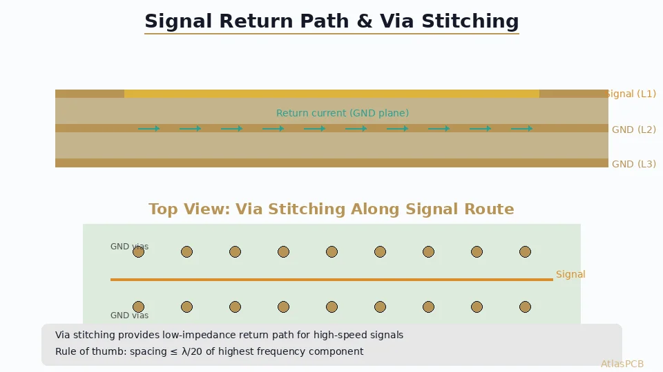
Ground guard traces: A grounded trace between two signal traces can provide 10–20 dB additional isolation, IF the guard trace is stitched to ground with vias at ≤λ/20 spacing. Without ground vias, a guard trace can actually increase coupling.
Differential signaling: Differential pairs are inherently more immune to common-mode crosstalk. The differential receiver rejects common-mode noise.
Reduce rise time (if possible): Slower edges have less high-frequency energy and generate less crosstalk. However, this is usually not a design choice in high-speed interfaces.
Via Stubs and Their Impact
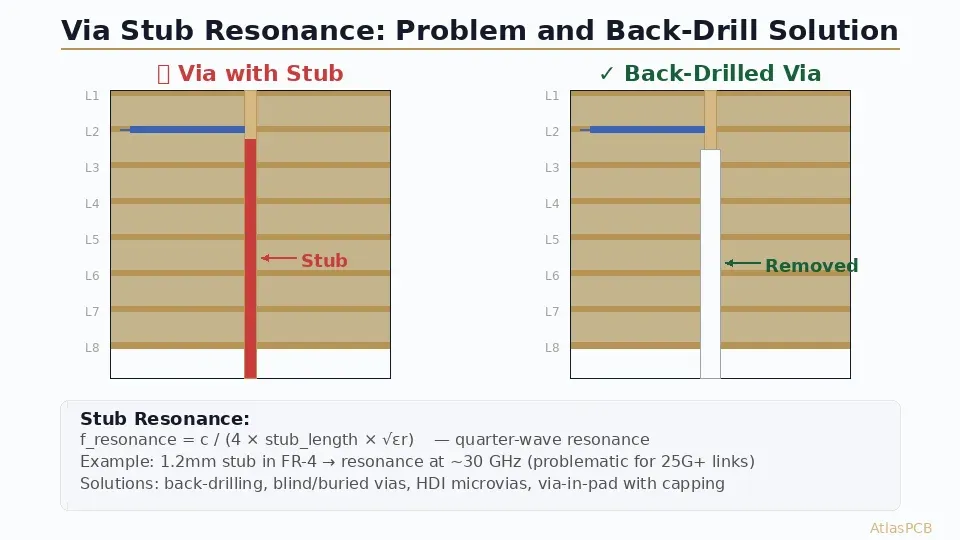
The Via Stub Problem
When a signal via connects two inner layers but passes through the entire board, the unused portion of the via barrel forms a stub. This stub acts as an unterminated transmission line that resonates at its quarter-wave frequency:
f_resonance = c / (4 × L_stub × √Dk)
Where L_stub is the physical stub length and Dk is the effective dielectric constant surrounding the via.
Example: A through-hole via in a 2.0 mm thick board connecting Layer 2 to Layer 3 (at 0.3 mm depth) has a stub length of approximately 1.7 mm. In FR-4 (Dk ≈ 4.0):
f_resonance = (3 × 10¹¹ mm/s) / (4 × 1.7 mm × √4.0) = 22 GHz
The signal experiences a deep notch (null) at 22 GHz and odd harmonics. For a 25 Gbps NRZ signal (Nyquist frequency = 12.5 GHz), this notch falls right in the signal bandwidth and causes severe eye closure.
Via Stub Mitigation
Back-drilling: The most common production solution. After the board is fabricated, a controlled-depth drill removes the unused stub portion. Typical back-drill accuracy is ±0.1 mm, leaving a residual stub of 0.1–0.2 mm (which resonates at >75 GHz—well above most signal bandwidths). See our [back-drill guide]/blog/pcb-back-drill/) for details.
Blind/buried vias: Use blind vias that connect only the required layers, eliminating the stub entirely. More expensive but provides the cleanest signal path. Essential for HDI designs.
Via optimization in routing:
- Place signal vias to minimize stub length (route on layers closest to the via entry point)
- Use consistent via structures for differential pairs
- Locate return path vias adjacent to signal vias (within 0.5 mm)
Via Impedance
A plated through-hole via typically has a characteristic impedance of 25–35 Ω—much lower than the 50 Ω trace. This impedance mismatch causes reflections even without a stub. Mitigation:
- Anti-pad sizing: Larger anti-pads increase via impedance. A 0.3 mm drill with a 0.7 mm anti-pad in a 0.1 mm dielectric yields approximately 45–50 Ω.
- Via pad reduction: Minimize via pad diameter (landing pad only, no thermal relief on signal layers)
- Backfill: Non-functional pads should be removed on inner layers for high-speed vias
Return Path Management
The Physics of Return Current
Every signal current must return to its source. At DC and low frequencies, return current follows the path of least resistance (spreading across the ground plane). At frequencies above approximately 1 MHz, return current follows the path of least inductance—directly beneath the signal trace on the nearest reference plane.
The signal and its return current form a current loop. The area of this loop determines:
- Inductance: Larger loop → higher inductance → higher impedance
- EMI radiation: Larger loop → stronger electromagnetic radiation
- Crosstalk: Signals sharing return path disruptions couple through common impedance
Ground Plane Discontinuities
Slots and splits: A slot in the ground plane beneath a signal trace forces return current to detour around the slot, dramatically increasing loop area. At 1 GHz, even a 2 mm slot can cause 20+ dB degradation in EMC performance.
Clearance voids: Through-hole via anti-pads create clearance voids in ground planes. Dense via fields can create Swiss-cheese ground planes with significantly increased impedance. Use stitching vias to maintain ground continuity around clearance areas.
Split planes: If power or ground planes must be split, NEVER route high-speed signals across the split boundary. If crossing is unavoidable, provide a low-impedance bridge (decoupling capacitors or stitching capacitors) at the crossing point.
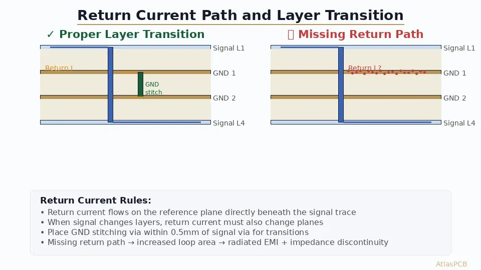
Layer Transitions and Return Path
When a signal transitions from one layer to another via a via, the reference plane typically changes. The return current must also transition, and ground stitching vias provide this path.
Design rules for return path vias:
- Place ≥2 ground vias within 0.5 mm of every high-speed signal via
- Ground vias should connect the reference planes of both the source and destination layers
- For differential pairs, place ground vias between and on both sides of the signal via pair
- For layer transitions where the reference changes from ground to power, add a decoupling capacitor between ground and power at the transition point
Practical Design Rules Summary
Impedance
| Rule | Recommendation |
|---|---|
| Target tolerance | ±10% standard, ±7% for high-speed serial |
| Calculation method | 2D field solver, validated with fabricator |
| Trace width adjustment | After layout, verify with impedance extraction |
| Test coupons | Include on every panel per IPC-2141 |
Crosstalk
| Rule | Recommendation |
|---|---|
| Minimum spacing (digital) | ≥2× dielectric height (2H) |
| Minimum spacing (sensitive) | ≥3× dielectric height (3H) |
| Preferred routing layer type | Stripline (FEXT ≈ 0) |
| Guard traces | Only effective with ground stitching vias |
| Length matching segments | Avoid serpentine overlap; maintain spacing |
Via Design
| Rule | Recommendation |
|---|---|
| Stub length limit | <0.25 mm for 10+ Gbps signals |
| Back-drill tolerance | ±0.1 mm (specify target stub) |
| Return via placement | ≤0.5 mm from signal via |
| Differential pair vias | Matched structure, symmetrical ground vias |
| Anti-pad optimization | Size for target via impedance |
Return Path
| Rule | Recommendation |
|---|---|
| Ground plane continuity | No slots or splits under high-speed traces |
| Ground stitching | ≤λ/20 spacing in high-speed areas |
| Layer transition | ≥2 return vias per signal via |
| Reference plane change | Decoupling cap if GND↔PWR change |
SI Simulation Workflow
For designs operating at 10+ Gbps or with tight timing margins:
Pre-Layout
- Stackup optimization: Define layer count, dielectric materials, and thicknesses to achieve target impedance while meeting crosstalk spacing constraints.
- Channel budget: Calculate insertion loss budget from transmitter to receiver, allocating loss to traces, vias, connectors, and AC coupling capacitors.
- Topology analysis: Determine if equalization (CTLE, DFE) is needed based on the channel loss budget.
Post-Layout
- Impedance extraction: Verify impedance of routed traces against targets.
- Crosstalk analysis: Simulate worst-case aggressor combinations. Include power-supply-induced jitter (PSIJ) if relevant.
- Via simulation: Extract S-parameters for critical signal vias. Verify no resonances within the signal bandwidth.
- Eye diagram simulation: Run statistical or bit-by-bit simulation to verify eye opening meets mask requirements (e.g., PCIe Gen 5 COM metric, 100G Ethernet ERL).
- Timing analysis: Verify setup/hold timing for parallel buses (DDR5, etc.).
Common SI Mistakes to Avoid
- Routing high-speed signals on outer layers without ground plane beneath: Creates an uncontrolled impedance microstrip with excessive radiation.
- Splitting ground planes under high-speed signal areas: Disrupts return current path and creates slot antennas.
- Ignoring via stubs: At 10+ Gbps, undrilled stubs are a primary cause of channel failure.
- Using 90° trace bends: Creates impedance discontinuities. Use 45° chamfer or arc bends.
- Mismatched differential pair via structures: Using different via types for P and N legs creates common-mode conversion and skew.
- Neglecting copper roughness: At high frequencies, rough copper foil (standard profile) increases loss by 20–50% compared to smooth foil. Specify low-profile (LP) or very-low-profile (VLP) copper for high-speed layers.
- Inadequate decoupling: Insufficient power plane decoupling causes PDN noise that couples into signal paths through return current.
Conclusion
Signal integrity is not a single technique but a holistic design discipline. Impedance control, crosstalk management, via optimization, and return path continuity are interdependent—a failure in any one area can undermine the others. Modern designs at 25–112 Gbps per lane demand attention to all four pillars simultaneously.
At Atlas PCB , we support signal integrity requirements through precise impedance control (±7% available), back-drill capability (±0.1 mm), HDI blind/buried vias, and advanced materials for low-loss transmission lines. Get a quote for your next high-speed design.
For related topics, see our guides on [controlled impedance PCB]/blog/controlled-impedance-pcb/), [differential pair routing]/blog/differential-pair-routing-pcb/), and [high-speed PCB design]/blog/high-speed-pcb-design/).
Further Reading
- [HDI PCB Design Guide: Stackup Rules, Via Structures & DFM Checklist]/blog/hdi-pcb-design-guide/)
- [Blind Via vs Buried Via: Design Rules, Cost Impact & When to Use Each]/blog/blind-via-vs-buried-via/)
- [Microstrip vs Stripline: Routing Strategies for Controlled Impedance PCBs]/blog/microstrip-vs-stripline/)
- [PCB DFM Checklist: 50 Points to Review Before Sending Gerbers]/blog/pcb-dfm-checklist/)
- [EMC/EMI Design for PCBs: Passing Compliance on the First Try]/blog/emc-emi-pcb-design/)
About AtlasPCB — We specialize in complex PCB manufacturing for HDI, RF, and high-reliability applications. Explore our impedance-controlled PCB manufacturing . Every order includes free engineering review. Get your quote.
Reviewed by AtlasPCB Engineering Team — IPC-certified manufacturing specialists with 15+ years of production experience in HDI, RF, and high-reliability PCB fabrication. Content based on factory floor data and real customer design reviews.
- signal integrity
- impedance control
- crosstalk
- via stub
- return path
- high-speed PCB