· AtlasPCB Engineering · Engineering · 9 min read
PCB Back Drill: Why, When, and How to Specify It
Technical guide to PCB back drilling for high-speed signal integrity. Covers via stub effects, when back drilling is needed, depth control, design rules, and cost considerations for multi-gigabit applications.

Via stubs are invisible parasites in your signal path. They do nothing useful — they are the unused portion of a plated through-hole via that extends beyond the signal layer into empty board space. At low frequencies, stubs are harmless. At 5GHz and above, they become resonant structures that create insertion loss notches, degrading or destroying multi-gigabit signals.
Back drilling removes the stub. This guide covers when you need it, how it works, and how to specify it.
The Via Stub Problem
What Creates a Stub
When a signal transitions from Layer 1 to Layer 3 through a plated through-hole via in a 16-layer board, the via extends from Layer 1 to Layer 16 — but only the portion from Layer 1 to Layer 3 carries signal. The remaining portion (Layer 3 to Layer 16) is the stub.
L1  ───►  Via  ◄─── Signal enters here
L2        │
L3  ───►  Via  ◄─── Signal exits here
L4        │
L5        │
...       │     ◄─── This is the STUB
L14       │         (unused via length)
L15       │
L16  ─────┘
Why Stubs Cause Problems
A via stub behaves as a shorted transmission line. It has a resonant frequency where it presents very low impedance to the signal — effectively a short circuit at that frequency:
f_resonance ≈ c / (4 × L_stub × √Dk_eff)Where:
- c = speed of light (3×10⁸ m/s)
- L_stub = stub length
- Dk_eff = effective dielectric constant (~3.8-4.2 for FR4)
Stub Resonance Table
| Stub Length | Resonance Frequency | Signal Degradation Starts | Critical For |
|---|---|---|---|
| 20 mil (0.5mm) | ~37 GHz | ~12 GHz | 56G/112G PAM4 |
| 40 mil (1.0mm) | ~18 GHz | ~6 GHz | 25G NRZ, 56G PAM4 |
| 60 mil (1.5mm) | ~12 GHz | ~4 GHz | 10G+ NRZ |
| 80 mil (2.0mm) | ~9 GHz | ~3 GHz | 10G NRZ marginal |
| 100 mil (2.5mm) | ~7.5 GHz | ~2.5 GHz | 5G+ affected |
| 120 mil (3.0mm) | ~6 GHz | ~2 GHz | Problem for most high-speed |
| 200 mil (5.0mm) | ~3.7 GHz | ~1.2 GHz | Backplane stub — critical |
Rule of thumb: Signal degradation begins at approximately 1/3 of the stub resonance frequency. A 100mil stub resonates at 7.5GHz but begins degrading signals around 2.5GHz.
Insertion Loss Impact
For a 25Gbps NRZ signal (Nyquist frequency 12.5GHz) with a 60mil via stub:
| Frequency | Insertion Loss (no stub) | Insertion Loss (60mil stub) | Degradation |
|---|---|---|---|
| 1 GHz | -0.1 dB | -0.1 dB | None |
| 5 GHz | -0.3 dB | -0.8 dB | -0.5 dB |
| 10 GHz | -0.5 dB | -3.2 dB | -2.7 dB |
| 12.5 GHz | -0.6 dB | -8.5 dB | -7.9 dB |
| 15 GHz | -0.7 dB | -15+ dB | Resonance null |
At 12.5GHz (the Nyquist frequency of 25Gbps NRZ), a 60mil stub costs 7.9 dB of insertion loss. This is catastrophic for signal integrity — most SerDes receivers need the channel loss below 20-25 dB total.
How Back Drilling Works
The Process
Back drilling (also called controlled-depth drilling or stub removal) is a second drilling operation performed after the board is fully fabricated:
- Standard fabrication — Board is manufactured normally with plated through-hole vias
- Registration — Board is mounted on the drill machine with X-ray alignment to locate via positions
- Controlled-depth drilling — A larger-diameter drill enters from the opposite side, removing the plated copper and stub portion
- Depth verification — Cross-section or X-ray confirms residual stub length
Drill Parameters
| Parameter | Typical Value | Notes |
|---|---|---|
| Back drill diameter | Via drill + 8-12mil (0.2-0.3mm) | Must clear the plated hole wall |
| Depth tolerance | ±4 mil (±100μm) | Production standard |
| Residual stub target | 5-10 mil (125-250μm) | Balance: shorter = better SI, but risk of damage |
| Minimum clearance to signal layer | 5 mil (125μm) | Safety margin to prevent layer damage |
| Registration accuracy | ±2 mil (±50μm) | X-ray aligned |
Back Drill Diameter Selection
The back drill must be large enough to completely remove the plated copper on the via wall:
| Original Via Drill | Plated Hole Diameter | Recommended Back Drill |
|---|---|---|
| 8 mil (0.20mm) | 6 mil (0.15mm) | 18-20 mil (0.45-0.50mm) |
| 10 mil (0.25mm) | 8 mil (0.20mm) | 20-22 mil (0.50-0.55mm) |
| 12 mil (0.30mm) | 10 mil (0.25mm) | 22-24 mil (0.55-0.60mm) |
| 14 mil (0.35mm) | 12 mil (0.30mm) | 24-26 mil (0.60-0.65mm) |
| 16 mil (0.40mm) | 14 mil (0.35mm) | 26-28 mil (0.65-0.70mm) |
Engineer’s Note: The back drill hole must clear the plated barrel on all sides, accounting for drill registration tolerance (±2mil) and original via position tolerance (±2mil). Add at least 4mil per side to the plated hole diameter.

When to Specify Back Drilling
Decision Matrix
| Signal Type | Data Rate | Via Stub Length | Back Drill Needed? |
|---|---|---|---|
| SPI/I2C/UART | <100 Mbps | Any | No |
| DDR4 | 3.2 GT/s | <60 mil | No |
| USB 3.0 | 5 Gbps | <40 mil | Usually no |
| PCIe Gen3 | 8 GT/s | <40 mil | Marginal (depends on channel budget) |
| 10G Ethernet | 10.3125 Gbps | >30 mil | Yes |
| PCIe Gen4 | 16 GT/s | >20 mil | Yes |
| 25G Ethernet | 25.78125 Gbps | >15 mil | Yes |
| PCIe Gen5 | 32 GT/s | >10 mil | Yes |
| 56G PAM4 | 56 Gbps | >10 mil | Yes |
| 112G PAM4 | 112 Gbps | >5 mil | Yes (or use blind vias) |
Backplane-Specific Considerations
Server and networking backplanes are the primary application for back drilling:
- Board thickness: 100-250 mil (2.5-6.35mm)
- Layer count: 16-40+ layers
- Via stubs: often 100-200mil (50-80% of board thickness)
- Signal rates: 25G-112G per lane
Without back drilling, these stubs make multi-gigabit signaling physically impossible. Back drilling is a standard line item on every high-speed backplane BOM.
Design Rules for Back Drilling
Pad and Anti-Pad Sizing
The back drill hole is larger than the original via — ensure adequate anti-pad clearance on all layers that will be back-drilled:
| Layer | Anti-Pad Requirement |
|---|---|
| Back-drilled layers (no connection) | Anti-pad ≥ back drill diameter + 16mil (8mil per side clearance) |
| Signal connection layers | Standard anti-pad (not back-drilled) |
| Reference planes | Anti-pad ≥ back drill diameter + 16mil |
Example: For a 12mil via with 24mil back drill:
- Standard anti-pad on connection layers: 24mil (12mil drill + 6mil annular ring per side)
- Back-drill anti-pad on all other layers: 40mil (24mil back drill + 8mil clearance per side)
Drill-to-Drill Spacing
Back drill holes need adequate spacing to prevent structural weakness:
| Minimum Spacing | Condition |
|---|---|
| Back drill diameter + 10mil | Between two back drill holes |
| Back drill diameter + 8mil | Back drill to any other via |
| Back drill diameter + 12mil | Back drill to board edge |
Back Drill from Both Sides
Some designs require back drilling from both sides of the board — for example, when signals route on middle layers of a thick board:
Back drill from TOP side (removes stub above L8)
         ↓
L1   ────┐
L2       │  ← Back drilled from top
L3       │
L4       │
L5       │
L6       │
L7       │
L8   ────┤  ← Signal layer
L9       │
L10      │  ← Back drilled from bottom
L11      │
L12  ────┘
         ↑
Back drill from BOTTOM side (removes stub below L8)
Dual-side back drilling requires two registration setups and two drill passes — cost increases by approximately 30-50% over single-side back drilling.
Alternatives to Back Drilling
| Method | Stub Removal | Cost Impact | Limitations |
|---|---|---|---|
| Back drilling | Removes to ~5mil residual | +5-15% board cost | Minimum residual stub |
| Blind vias | No stub at all | +30-60% board cost | Aspect ratio limits |
| HDI microvias | No stub | +50-200% board cost | Layer count restrictions |
| Through-via (no treatment) | Full stub | Baseline | Signal degradation >3-5GHz |
| Shorter via (thinner board) | Reduced stub | May not be possible | Board thickness constrained by connector |
Back drilling is the most cost-effective solution for high-speed through-hole vias in boards >8 layers. Blind vias and HDI eliminate stubs entirely but at significantly higher cost.
When to Use Blind Vias Instead
- Stub residual from back drilling (5-10mil) is unacceptable (112G+ channels)
- Via count is low enough that blind via cost is manageable
- Board already requires HDI for other reasons (fine-pitch BGAs)
Verification and Quality Control
Depth Verification Methods
| Method | Accuracy | When Used |
|---|---|---|
| Cross-section (destructive) | ±1 mil | First article, periodic verification |
| X-ray measurement | ±2-3 mil | 100% production screening |
| Depth-sensing drill spindle | ±3-4 mil | Real-time during drilling |
| Electrical testing (stub resonance) | Indirect | Advanced — measures stub effect directly |
Acceptance Criteria
| Parameter | Specification |
|---|---|
| Residual stub length | 5-10 mil (or per design spec) |
| Depth tolerance | ±4 mil from target |
| Concentricity | Back drill centered within ±3mil of original via |
| No damage to signal layer | Cross-section verified: no copper removal on signal layer |
| No damage to reference plane | Cross-section verified: reference plane intact |
| Hole wall quality | No burrs, no loose plating fragments |
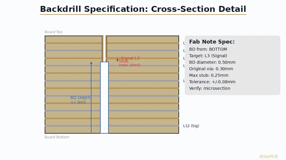
Specifying Back Drilling in Your Fab Drawing
Include the following in your fabrication notes:
BACK DRILL REQUIREMENTS:
- All vias marked "BD" in drill file shall be back drilled
- Back drill from [TOP/BOTTOM/BOTH] side(s)
- Back drill target: remove stub to within 10 mil of [Layer X]
- Back drill diameter: [XX] mil
- Residual stub tolerance: +5/-0 mil from target layer
- Depth tolerance: ±4 mil
- Verification: cross-section on first article + X-ray on production
Provide a separate drill file or drill table for back drill locations. Clearly mark which vias require back drilling — not all vias need it (only those carrying high-speed signals).
Design Checklist for Back Drilling
- Identify all vias carrying signals >5GHz (or >10Gbps NRZ / >25Gbps PAM4)
- Calculate stub length for each critical via
- Verify stub resonance frequency vs. signal bandwidth
- Size anti-pads on all back-drilled layers (back drill diameter + 16mil)
- Verify back drill diameter clears plated barrel (including registration tolerance)
- Check drill-to-drill spacing (back drill + 10mil minimum)
- Determine single-side or dual-side back drilling
- Specify residual stub target in fab notes (5-10mil typical)
- Create separate back drill file or mark in drill legend
- Request cross-section verification on first article
How Atlas PCB Handles Back Drilling
Atlas PCB performs back drilling on high-layer-count boards from 8 to 68 layers, using X-ray-aligned CNC drilling with laser depth sensing. We routinely process backplanes and high-speed digital boards for data center, networking, and telecom applications.
Atlas PCB achieves ±4mil back drill depth tolerance with X-ray registration, supports single-side and dual-side back drilling, and provides cross-section verification on every first article. Every back-drilled order includes our 12-hour human engineering review — we verify stub lengths, anti-pad sizing, and back drill clearances against your signal integrity requirements before production.
For designs requiring tighter than ±4mil tolerance, we offer enhanced process control with 100% X-ray depth verification.
Summary
- Via stubs are unused through-hole via portions that resonate and destroy signals above 3-5GHz
- Back drilling removes the stub, leaving 5-10mil residual — the most cost-effective stub mitigation
- Required for 10G+ Ethernet, PCIe Gen4/5, 25G/56G/112G SerDes, high-speed backplanes
- Depth tolerance ±4mil is production standard; specify 5-10mil residual stub target
- Anti-pad sizing must account for larger back drill diameter + registration tolerance
- Always verify with cross-section on first article
Building a high-speed backplane or 10G+ design? Upload your Gerbers for a free engineering review — we will verify your back drill specifications, stub analysis, and signal integrity requirements.
Related guides: [High-Speed PCB Design]/blog/high-speed-pcb-design/) | [Multilayer PCB Stackup Design Guide]/blog/multilayer-pcb-stackup-design-guide/) | [Controlled Impedance PCB]/blog/controlled-impedance-pcb/) | [HDI PCB Design Guide]/blog/hdi-pcb-design-guide/)
Further Reading
[HDI PCB Technology: Microvias, Laser Drilling, and High-Density Design]/blog/hdi-pcb-technology/)
[Blind Via vs Buried Via: Design Rules, Cost Impact & When to Use Each]/blog/blind-via-vs-buried-via/)
[High-Speed PCB Design: Signal Integrity Essentials for Modern Electronics]/blog/high-speed-pcb-design/)
[PCB Manufacturer with Engineering Review: Why Human DFM Audit Matters]/blog/pcb-manufacturer-engineering-review/)
[PCB DFM Checklist: 50 Points to Review Before Sending Gerbers]/blog/pcb-dfm-checklist/)
About AtlasPCB — We specialize in complex PCB manufacturing for HDI, RF, and high-reliability applications. Explore our impedance-controlled PCB manufacturing, or get an full PCB manufacturing capabilities . Every order includes free engineering review. Get your quote.
Reviewed by AtlasPCB Engineering Team — IPC-certified manufacturing specialists with 15+ years of production experience in HDI, RF, and high-reliability PCB fabrication. Content based on factory floor data and real customer design reviews.
- back drill
- via stub
- signal integrity
- high speed pcb
- pcb manufacturing
- controlled depth drilling