· AtlasPCB Engineering · Engineering · 12 min read
PCB Warpage Control: Causes, IPC Limits, and Prevention in Multilayer Boards
In-depth guide to PCB warpage causes including CTE mismatch, copper imbalance, and reflow stress. Learn IPC-6012 warpage limits, copper balancing techniques, symmetric stackup design, and material selection strategies.
PCB Warpage Control: Causes, IPC Limits, and Prevention in Multilayer Boards
A flat PCB is not a luxury — it’s a manufacturing requirement. When a board warps, surface-mount components cannot be placed accurately, BGA solder joints fail to form properly, automated optical inspection produces false readings, and the board may not even fit into its enclosure. For multilayer PCBs with fine-pitch components, warpage control is not just desirable; it’s essential for production yield.
This article examines the physics behind PCB warpage, the specific IPC limits that govern acceptance, and the practical engineering techniques that prevent warpage from occurring in multilayer designs.
Understanding PCB Warpage
Definitions: Bow vs. Twist
IPC-T-50 defines two distinct types of warpage:
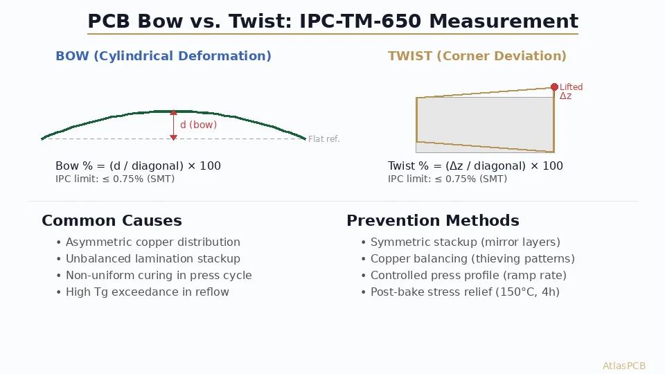
Bow is a cylindrical curvature of the board. Imagine holding a board at its edges — if it curves upward (or downward) along one axis while remaining straight along the perpendicular axis, that’s bow. Measured as the maximum deviation from a flat reference surface, expressed as a percentage of the board’s diagonal length.
Twist is a helical deformation where opposing corners lift in different directions. If you place the board on a flat surface, two diagonally opposite corners touch the surface while the other two corners are elevated. Twist is measured as the maximum height of the lifted corner divided by the diagonal length.
Total warpage is the combined effect of bow and twist, measured per IPC-TM-650 Method 2.4.22.
Warpage (%) = Maximum Deflection ÷ Board Diagonal Length × 100
IPC-6012 Warpage Limits
IPC-6012 Rev F specifies:
| Assembly Type | Maximum Bow & Twist |
|---|---|
| Surface Mount (SMT) | 0.75% |
| Through-Hole Only | 1.5% |
For a 100 mm × 100 mm board (diagonal ≈ 141 mm):
- SMT limit: 141 × 0.0075 = 1.06 mm maximum deflection
- TH limit: 141 × 0.015 = 2.12 mm maximum deflection
For a 300 mm × 200 mm board (diagonal ≈ 361 mm):
- SMT limit: 361 × 0.0075 = 2.71 mm maximum deflection
While 2.71 mm may sound generous, realize that this is measured across the entire diagonal. Local warpage in the BGA area can be far more critical. Many OEMs and EMS providers impose tighter limits:
- BGA area: 0.3–0.5% local warpage
- Fine-pitch (≤0.4 mm) BGA: Some require ≤0.2% local warpage
- JEDEC J-STD-020: Specifies package-level warpage limits that effectively constrain board-level warpage in the component zone
The Physics of Warpage
Coefficient of Thermal Expansion (CTE) Mismatch
Every material expands when heated. The rate of expansion, expressed in parts per million per degree Celsius (ppm/°C), is the CTE. The fundamental problem in PCBs is that the materials inside them have different CTEs:
| Material | CTE (XY plane) | CTE (Z-axis) |
|---|---|---|
| Copper | 17 ppm/°C | 17 ppm/°C |
| Standard FR-4 (Tg 130°C) | 14–17 ppm/°C | 50–70 ppm/°C |
| High-Tg FR-4 (Tg 170°C) | 12–15 ppm/°C | 40–55 ppm/°C |
| Polyimide | 12–16 ppm/°C | 35–50 ppm/°C |
| Low-CTE laminate (e.g., Megtron 6) | 9–12 ppm/°C | 25–40 ppm/°C |
In the XY plane, copper and FR-4 have reasonably similar CTEs (14–17 ppm/°C), and the glass fiber weave constrains expansion. But when copper is distributed unevenly — more copper on the top half of the board than the bottom — the two halves expand differently when heated. The copper-heavy side expands less (copper constrains the resin), while the copper-light side expands more. This differential expansion curves the board.
The Bimetallic Strip Effect
A PCB with unbalanced copper is essentially a bimetallic strip. During heating (lamination press, reflow oven), the side with less copper expands more, and the board bows toward the copper-heavy side. During cooling, the stresses reverse, but if the resin has passed through its glass transition temperature (Tg) and partially relaxed, the deformation becomes partially permanent.
This is why boards often warp after reflow even if they were flat before — the reflow temperature (typically 245–260°C peak for lead-free) is well above the Tg of standard FR-4 (130°C) and even high-Tg materials (170°C). Above Tg, the resin softens and the internal stresses redistribute.
Moisture Effects
FR-4 absorbs moisture from the atmosphere — typically 0.1–0.3% by weight over days to weeks in ambient conditions. This moisture:
- Causes differential swelling (layers with more resin swell more)
- Generates steam during reflow, creating internal pressure
- Can cause delamination, which itself creates warpage
IPC-J-STD-033 governs moisture sensitivity and bake-out requirements. Boards stored in uncontrolled environments should be baked at 105–125°C for 2–6 hours before reflow to drive out absorbed moisture.
Primary Causes of Warpage in Multilayer PCBs
1. Copper Imbalance
This is the single most common cause of warpage in multilayer boards. Copper imbalance occurs when:
- Gross copper area differs between the top and bottom halves of the stackup
- One side has large ground/power planes while the other has sparse signal routing
- Copper distribution within a layer is uneven (e.g., dense copper on one side of the board, open areas on the other)
For a well-detailed discussion on techniques to address this, see our guide on [copper balancing techniques]/blog/pcb-copper-balancing-techniques/).
How much imbalance causes problems? As a rule of thumb, a copper density difference of more than 15–20% between the top half and bottom half of the stackup will produce measurable warpage. For boards larger than 200 mm in any dimension, even a 10% imbalance can be problematic.
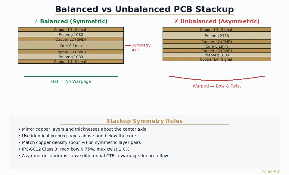
2. Asymmetric Stackup
Even if copper density is balanced, an asymmetric stackup creates warpage. Asymmetry includes:
- Unequal dielectric thicknesses above and below the board center
- Different prepreg styles (e.g., 1080 vs. 2116) on opposing sides
- Unequal number of prepreg plies above vs. below
A symmetric stackup means that the layer arrangement mirrors itself about the center. For an 8-layer board: L1/L2/L3/L4 should mirror L5/L6/L7/L8 in both copper weight and dielectric thickness.
3. Glass Weave Style Mismatch
Prepreg glass weave styles have different CTEs and resin content:
| Weave Style | Thickness (cured) | Resin Content |
|---|---|---|
| 106 | ~50 µm | 65–75% |
| 1080 | ~65 µm | 60–70% |
| 2116 | ~115 µm | 48–55% |
| 7628 | ~180 µm | 42–48% |
Higher resin content means higher Z-axis CTE and more potential for warpage. Using different weave styles on opposite sides of the stackup creates CTE asymmetry. Best practice: use the same prepreg construction on both sides of the center, as detailed in our [multilayer PCB manufacturing process guide]/blog/multilayer-pcb-manufacturing-process-explained/).
4. Reflow Thermal Profile
The reflow profile significantly affects warpage behavior:
- Ramp rate: Faster ramps create larger thermal gradients through the board thickness, increasing transient warpage
- Peak temperature: Higher peaks (necessary for lead-free) soften the resin more, allowing greater deformation
- Time above liquidus: Longer exposure above ~217°C (SAC305) gives the board more time to warp
- Cooling rate: Rapid cooling freezes warpage in place; slow cooling allows some stress relaxation
Studies by JEDEC and others show that board warpage increases significantly above Tg, peaks near the solder melting point, and partially recovers during cooling. The net warpage after reflow is typically 30–60% of the peak warpage observed during the heating phase.

Prevention Strategies
Strategy 1: Symmetric Stackup Design
The most fundamental warpage prevention measure is designing a stackup that is symmetric about the center plane. Symmetry applies to:
- Copper weights: If L1 is 1 oz, the bottom layer should also be 1 oz
- Dielectric materials: Same prepreg type and number of plies above and below center
- Core placement: Center the core in the middle of the stackup
Example — Symmetric 8-Layer Stackup:
L1  (Signal)    — 1 oz copper
    Prepreg     — 2×1080
L2  (Ground)    — 1 oz copper
    Core        — 0.2 mm
L3  (Signal)    — 0.5 oz copper
    Prepreg     — 1×2116
--- CENTER PLANE ---
    Prepreg     — 1×2116
L4  (Signal)    — 0.5 oz copper
    Core        — 0.2 mm
L5  (Ground)    — 1 oz copper
    Prepreg     — 2×1080
L6  (Signal)    — 1 oz copper
Wait — this 8-layer example only shows 6 layers. Let’s correct with a proper 8-layer symmetric structure:
L1  (Signal)    — 1 oz copper
    Prepreg     — 2×1080
L2  (Ground)    — 1 oz copper
    Core        — 0.2 mm
L3  (Signal)    — 0.5 oz copper
    Prepreg     — 1×2116
L4  (Power)     — 1 oz copper
--- CENTER PLANE ---
L5  (Power)     — 1 oz copper
    Prepreg     — 1×2116
L6  (Signal)    — 0.5 oz copper
    Core        — 0.2 mm
L7  (Ground)    — 1 oz copper
    Prepreg     — 2×1080
L8  (Signal)    — 1 oz copper
Notice the mirror: L1↔L8, L2↔L7, L3↔L6, L4↔L5 — all have matching copper weights and dielectric construction.
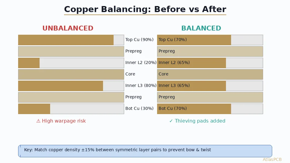
Strategy 2: Copper Balancing
Even with a symmetric stackup, copper density must be balanced. A ground plane at 90% copper fill and a signal layer at 20% fill are not equivalent even if they have the same copper weight.
Copper balancing techniques:
- Add copper fill (hatched or solid) to sparse signal layers to match the copper density of the corresponding mirror layer
- Use cross-hatched ground pours instead of solid fills if the mirror layer is a sparse signal layer (reduces the density of the ground layer to match)
- Target ±10% copper density match between mirrored layer pairs
- Balance within each layer: Avoid having all copper concentrated on one side of the board with open space on the other
Calculating copper density: Most EDA tools can report copper area per layer. Divide copper area by total board area to get the percentage. Compare L1 vs. L8 (or Ln vs. the mirror layer).
Strategy 3: Material Selection
Material choice significantly impacts warpage propensity. For warpage-critical designs, consider upgrading from standard FR-4 to materials with better thermal stability, as covered in our [material selection guide]/blog/pcb-material-selection-guide/):
| Material | Tg (°C) | Z-CTE (ppm/°C) below Tg | Warpage Risk |
|---|---|---|---|
| Standard FR-4 | 130–140 | 50–70 | High |
| Mid-Tg FR-4 | 150–160 | 45–55 | Medium |
| High-Tg FR-4 | 170–180 | 40–50 | Medium-Low |
| Polyimide | 250+ | 35–50 | Low |
| Low-CTE laminate | 200+ | 20–35 | Very Low |
Higher Tg means the resin remains rigid to a higher temperature, reducing the opportunity for thermal deformation during reflow. Lower Z-CTE means less Z-axis expansion, reducing the driving force for warpage.
Strategy 4: Panel Design and Breakaway Considerations
Board warpage is related to board size — larger boards warp more. Panel design affects warpage:
- Support rails: Wide breakaway rails (≥10 mm) add rigidity during reflow
- Tab routing vs. V-score: V-scored panels maintain more structural integrity during assembly than tab-routed panels
- Panel aspect ratio: Square panels warp less than long, narrow panels (bow mode is dominant along the long axis)
- Fiducial placement: Copper fiducials near panel edges can affect local copper balance
Strategy 5: Process Controls
Manufacturing process optimization is equally important:
Lamination:
- Controlled press profiles with uniform temperature distribution
- Proper pre-bake of inner layers (105°C, 1 hour minimum)
- Balanced prepreg layup in the press book
- Cool-down rate ≤3°C/minute from peak press temperature
Reflow:
- Minimize peak temperature (stay within solder paste specification)
- Minimize time above liquidus
- Use support fixtures or pallets for thin or large boards
- Consider nitrogen atmosphere to enable lower peak temperatures
Storage:
- Store bare boards in moisture-barrier bags with desiccant
- Bake boards per IPC-J-STD-033 if moisture exposure exceeds the allowed time
- Store boards flat, not on edge, to prevent gravity-induced creep
Measuring Warpage
Manual Measurement
Place the board on a known-flat surface (such as a granite surface plate) and use a feeler gauge or height gauge to measure the maximum gap between the board and the surface at multiple points. The maximum gap is the warpage deflection.
Automated Measurement
Shadow moiré and laser profiling systems provide full-surface warpage maps. These systems can measure warpage:
- At room temperature (post-manufacturing)
- In real-time during reflow (dynamic warpage measurement)
- Per IPC-TM-650 Method 2.4.22
Dynamic warpage measurement during reflow is particularly valuable because it reveals the peak warpage (which may be 2–3× the room-temperature value) and identifies the exact temperature at which warpage transitions from concave to convex or vice versa.
Warpage and BGA Reliability
For boards carrying BGA components, warpage is directly linked to solder joint reliability:
- During reflow: If the board warps concavely (center rises), the BGA corners lose contact with the paste, leading to open solder joints at the corners — the “smile” defect
- If the board warps convexly (edges rise), the BGA center joints are at risk — the “cry” defect
- After cooling: Residual warpage creates permanent stress on solder joints, accelerating fatigue cracking during thermal cycling
JEDEC JESD22-B112 specifies package warpage measurement methods that help predict these failure modes. For large BGAs (>25 mm), board warpage within the BGA footprint should be kept below 0.3%.
Case Study: Resolving Warpage in a 12-Layer Design
A 12-layer, 1.6 mm thick board measuring 180 mm × 120 mm exhibited 1.2% warpage after reflow — well above the 0.75% limit. Investigation revealed:
Root causes:
- L1 (signal): 35% copper density
- L12 (signal): 78% copper density (large ground pour)
- Prepreg above L2 was 2×1080; below L11 was 1×2116 + 1×1080
- No copper balancing on inner signal layers
Corrective actions:
- Added copper fill to L1 to raise density to 70%
- Adjusted prepreg to symmetric construction (2×1080 on both sides)
- Balanced inner signal layers L3↔L10 and L5↔L8 to within 10% density
- Specified high-Tg FR-4 (Tg 170°C) to reduce resin softening during reflow
Result: Post-reflow warpage reduced to 0.45% — well within specification.
Summary
PCB warpage is a predictable, preventable phenomenon when approached with engineering discipline:
- Design symmetric stackups — mirror layers about the center
- Balance copper density — within 10% between mirror pairs
- Select appropriate materials — higher Tg, lower CTE for critical applications
- Control moisture — bake boards before reflow per J-STD-033
- Optimize reflow profiles — minimize peak temperature and time above liquidus
- Measure and verify — use IPC-TM-650 2.4.22 or shadow moiré for quantitative data
Warpage control starts at the design stage and requires collaboration between the PCB designer, fabricator, and assembler. When these three stakeholders align on stackup design, material selection, and process parameters, warpage becomes a non-issue rather than a yield killer.
Ready to start your project? Upload your Gerbers for a free engineering review, or talk to an engineer about your design requirements.
Further Reading
- [AI Hardware PCB Thermal Management: Advanced Multilayer Stackup Design for 1000W+ Processing Units]/blog/ai-hardware-pcb-thermal-management-multilayer-design/)
- [Rogers PCB Fabrication: Material Sourcing, Lead Times & Quality Control]/blog/rogers-pcb-fabrication/)
- [PCB Rigid-Flex Bend Zone Reliability: Design Rules, Material Selection & Lifecycle Testing]/blog/pcb-rigid-flex-bend-zone-reliability/)
- [ENEPIG vs ENIG Surface Finish: Complete Comparison for Wire Bonding, Solderability, and Long-Term Reliability]/blog/enepig-vs-enig-surface-finish-wire-bonding/)
- [PCB Surface Finish Comparison: OSP vs HASL vs Immersion Silver vs ENIG for Assembly Reliability]/blog/pcb-surface-finish-osp-hasl-enig-immersion-silver-comparison/)
- Our Manufacturing Capabilities
About AtlasPCB — We specialize in complex PCB manufacturing for HDI, RF, and high-reliability applications. Explore our multilayer PCB fabrication up to 30 layers . Every order includes free engineering review. Get your quote.
Reviewed by AtlasPCB Engineering Team — IPC-certified manufacturing specialists with 15+ years of production experience in HDI, RF, and high-reliability PCB fabrication. Content based on factory floor data and real customer design reviews.
- warpage
- multilayer-pcb
- manufacturing
- reliability
- copper-balancing