· AtlasPCB Engineering · Engineering · 12 min read
PCB Copper Balancing Techniques: Prevent Warpage in Multilayer Board Design
Learn copper balancing techniques for multilayer PCBs including thieving patterns, fill strategies, and IPC-6012 bow/twist requirements to prevent warpage during lamination and reflow.
PCB Copper Balancing Techniques: Prevent Warpage in Multilayer Board Design
Every multilayer PCB designer has encountered it: a board that comes out of lamination with a visible curve, fails the flatness check at assembly, or — worst case — causes BGA solder joint opens after reflow. The root cause is almost always copper imbalance. When copper distribution across a multilayer stackup is asymmetric, differential thermal expansion during lamination press cooling and solder reflow creates internal bending moments that warp the board.
Copper balancing is not a cosmetic concern — it is a structural engineering requirement. IPC-6012 limits bow and twist to 0.75% for surface-mount assemblies, and high-density BGA designs often demand ≤ 0.5%. Achieving these limits in a 12+ layer board with mixed signal, power, and ground layers requires deliberate design strategies: symmetric stackups, copper thieving patterns, fill optimization, and coordination between the PCB designer and fabricator.
This guide covers the physics of copper-induced warpage, practical balancing techniques, IPC requirements, and design rules that eliminate warpage problems before they reach manufacturing.
Why Copper Imbalance Causes Warpage
The CTE Mismatch Problem
A multilayer PCB is a composite structure: copper foil (CTE ≈ 17 ppm/°C) laminated with FR-4 resin/glass (in-plane CTE ≈ 12-16 ppm/°C for the glass-constrained composite, but 55-70 ppm/°C for the resin alone). During lamination, the stackup is pressed at 180-190°C and then cooled to room temperature. During reflow, the assembled board reaches 250-260°C peak.
At every thermal transition, each layer expands and contracts differently based on its copper-to-resin ratio:
- A layer with 90% copper coverage behaves more like a copper sheet (low CTE)
- A layer with 10% copper coverage behaves more like FR-4 resin (higher CTE)
When these layers are on opposite sides of the board center, the differential contraction during cooling creates a bimetallic strip effect. The board curves toward the side with more copper (the side that contracted less).
Quantifying the Imbalance
The warpage tendency of a multilayer PCB can be approximated by the copper balance ratio for each mirrored layer pair:
Δ_copper = |Coverage_top_layer - Coverage_bottom_layer|
Where top/bottom refer to layers equidistant from the board center (L1 & L_n, L2 & L_{n-1}, etc.).
| Δ_copper per Layer Pair | Warpage Risk | Action Required |
|---|---|---|
| < 10% | Low | Standard process acceptable |
| 10-25% | Moderate | Add thieving to low-density layer |
| 25-50% | High | Redesign routing or add extensive thieving |
| > 50% | Critical | Stackup redesign required |
The cumulative effect across all layer pairs determines the total warpage. A board can tolerate one moderately imbalanced pair if all others are well-balanced, but multiple imbalanced pairs compound the problem.
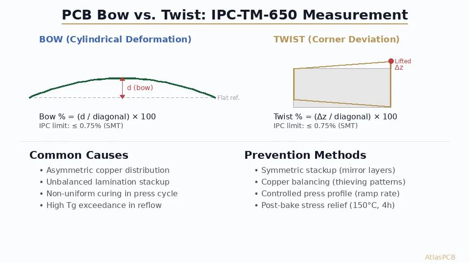
IPC-6012 Bow and Twist Requirements
Specification Limits
IPC-6012, “Qualification and Performance Specification for Rigid Printed Boards,” defines bow and twist limits:
| Board Type | IPC-6012 Class 2 | IPC-6012 Class 3 |
|---|---|---|
| SMT assembly (general) | ≤ 0.75% | ≤ 0.75% |
| Through-hole only | ≤ 1.5% | ≤ 1.5% |
| BGA ≤ 1.0mm pitch | ≤ 0.75% (≤ 0.5% recommended) | ≤ 0.50% |
| BGA ≤ 0.5mm pitch | ≤ 0.50% | ≤ 0.50% |
How Bow and Twist Are Measured
Per IPC-TM-650, Method 2.4.22:
- Place the board on a flat granite surface plate
- Board is free to assume its natural shape (no clamping)
- Bow = Maximum deviation from the surface plate in a single-axis curvature
- Twist = Maximum deviation when opposite corners are not coplanar
- Percentage = (Maximum deviation ÷ Diagonal length) × 100
Example: A 250mm × 200mm board has a diagonal of 320mm. At 0.75% limit, maximum allowable deviation = 320 × 0.0075 = 2.4mm.
For boards destined for [BGA pad design with fine-pitch components]/blog/pcb-pad-design-bga-qfn/), warpage directly impacts solder joint coplanarity and is a primary cause of head-in-pillow defects.
Copper Balancing Strategies
Strategy 1: Symmetric Stackup Architecture
The most fundamental copper balancing technique is designing a symmetric stackup — identical layer structure mirrored about the board center. This means:
- L1 mirrors L_n (same copper weight, similar routing density)
- L2 mirrors L_{n-1}
- Prepreg and core thicknesses are symmetric
- Copper weights match between mirrored pairs
Example: Well-balanced 8-layer stackup:
| Layer | Function | Cu Weight | Target Coverage |
|---|---|---|---|
| L1 | Signal | 1 oz (35μm) | 40-50% |
| L2 | Ground (solid) | 1 oz (35μm) | 85-90% |
| L3 | Signal | 0.5 oz (18μm) | 35-45% |
| L4 | Power (split) | 1 oz (35μm) | 70-80% |
| L5 | Power (split) | 1 oz (35μm) | 70-80% |
| L6 | Signal | 0.5 oz (18μm) | 35-45% |
| L7 | Ground (solid) | 1 oz (35μm) | 85-90% |
| L8 | Signal | 1 oz (35μm) | 40-50% |
L1 ↔ L8, L2 ↔ L7, L3 ↔ L6, L4 ↔ L5 — each pair has matching copper weight and similar coverage targets.
For detailed guidance on stackup architecture, see our [PCB stackup design guide]/blog/pcb-stackup-design-guide/).
Strategy 2: Copper Thieving Patterns
When routing density on mirrored layers inevitably differs, copper thieving equalizes the distribution by adding non-functional copper to sparse areas.
Crosshatch Thieving
The most common thieving pattern for [signal integrity-sensitive designs]/blog/signal-integrity-pcb-design-guide/):
- Pattern: Grid of copper lines with regular gaps
- Line width: 0.2-0.3mm (8-12 mil)
- Pitch: 1.0-1.27mm (40-50 mil)
- Effective fill: ~50% copper density
- Clearance to functional traces: ≥ 0.5mm (20 mil)
Crosshatch is preferred for signal layers because it does not create large unbroken copper areas that could affect impedance or create unintended coupling.
Dot Array Thieving
- Pattern: Regular array of circular copper dots
- Dot diameter: 0.5-0.8mm (20-32 mil)
- Center-to-center spacing: 1.0-1.5mm (40-60 mil)
- Effective fill: ~20-35% copper density
- Best for: Layers where even crosshatch might affect signal integrity
Solid Fill Thieving
- Pattern: Continuous copper pour in unused areas
- Connection: Tied to ground via thermal reliefs, or electrically isolated
- Effective fill: 80-95% copper density
- Best for: Ground and power layers, inner layers far from signal references
Rule of thumb: Choose the thieving pattern that brings the layer’s total copper coverage to within ±15% of its mirrored pair.
Strategy 3: Copper Pour Optimization
Beyond thieving, optimizing the functional copper pours on each layer improves balance:
- Ground planes: Use negative-plane (solid copper with clearances) rather than positive-plane (traces) to maximize coverage
- Power planes: Minimize splits; where splits are necessary, fill unused split zones with copper tied to the nearest power net
- Signal layers: Enable copper fill (ground pour) in all unused areas, with appropriate clearance rules

Strategy 4: Panel-Level Copper Balancing
Copper balance must be evaluated at the panel level, not just the individual board level. Manufacturing panels include:
- Working boards: The actual PCBs being fabricated
- Panel borders: Rails and tooling strips
- Breakaway tabs: Connections between boards and panel frame
- Coupon areas: Test coupons for impedance, plating, etc.
The panel border and inter-board areas should contain copper fill matching the average density of the working boards. Without this, the panel edges warp differently than the center, causing:
- Non-uniform lamination pressure
- Thickness variation across the panel
- Registration errors between layers
For more on panel design, see our [PCB panelization guide]/blog/pcb-panelization-guide/).
Layer-by-Layer Copper Analysis
How to Calculate Copper Coverage
Most EDA tools can report copper coverage percentage per layer. The calculation:
Coverage (%) = (Copper area on layer ÷ Total board area) × 100
Include:
- Traces and pads
- Copper pours and fills
- Thieving patterns
- Thermal relief spokes
Exclude:
- Annular ring area of non-plated holes
- Clearances and anti-pads
Target Coverage by Layer Type
| Layer Type | Typical Coverage | Target with Balancing |
|---|---|---|
| Solid ground plane | 80-95% | 85-90% |
| Split power plane | 60-85% | 75-85% (fill unused splits) |
| Dense signal layer | 30-50% | 45-55% (with thieving) |
| Sparse signal layer | 10-25% | 35-50% (with thieving) |
| Outer component layer | 25-45% | 40-50% (with ground pour) |
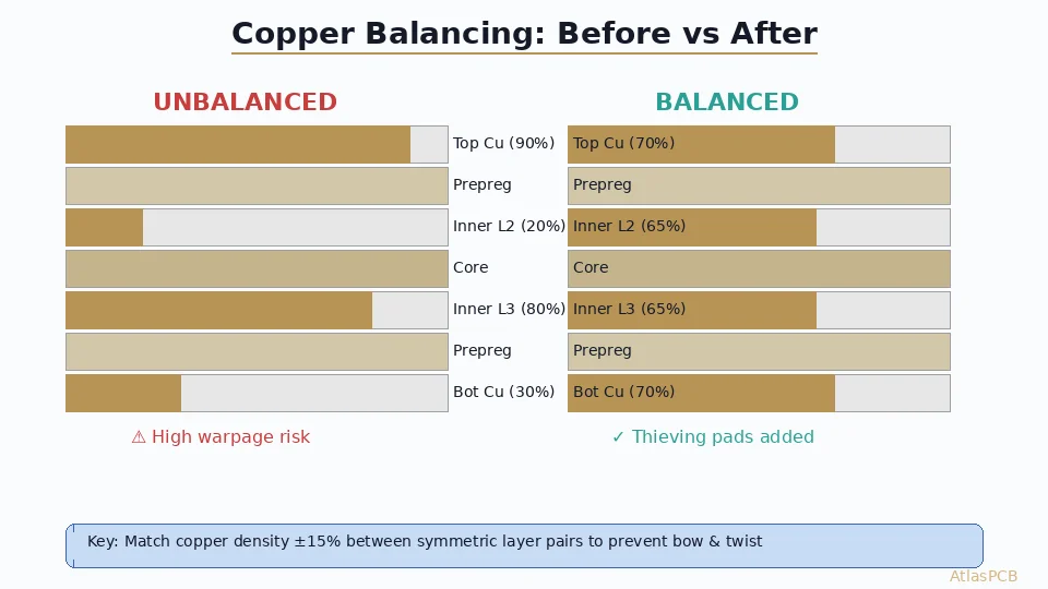
Worked Example: 12-Layer Imbalanced Design
Before copper balancing:
| Layer Pair | Top Layer | Coverage | Bottom Layer | Coverage | Δ |
|---|---|---|---|---|---|
| L1 ↔ L12 | Signal (dense) | 48% | Signal (sparse) | 18% | 30% ⚠️ |
| L2 ↔ L11 | Ground (solid) | 88% | Ground (solid) | 87% | 1% ✅ |
| L3 ↔ L10 | Signal | 32% | Signal | 29% | 3% ✅ |
| L4 ↔ L9 | Power (3 splits) | 62% | Power (solid) | 85% | 23% ⚠️ |
| L5 ↔ L8 | Signal | 25% | Signal | 41% | 16% ⚠️ |
| L6 ↔ L7 | Ground | 90% | Power | 72% | 18% ⚠️ |
Total warpage prediction: HIGH RISK — four pairs exceed 15% threshold.
After copper balancing:
| Layer Pair | Top Layer | Coverage | Bottom Layer | Coverage | Δ | Action Taken |
|---|---|---|---|---|---|---|
| L1 ↔ L12 | Signal | 48% | Signal + thieving | 44% | 4% ✅ | Crosshatch thieving on L12 |
| L2 ↔ L11 | Ground | 88% | Ground | 87% | 1% ✅ | None needed |
| L3 ↔ L10 | Signal | 32% | Signal | 29% | 3% ✅ | None needed |
| L4 ↔ L9 | Power (fills) | 78% | Power | 85% | 7% ✅ | Filled unused splits on L4 |
| L5 ↔ L8 | Signal + thieving | 40% | Signal | 41% | 1% ✅ | Crosshatch thieving on L5 |
| L6 ↔ L7 | Ground | 90% | Power + fill | 84% | 6% ✅ | Copper fill on L7 unused areas |
Total warpage prediction: LOW RISK — all pairs within 10%.
Thieving Pattern Design Rules
Clearance Requirements
Thieving copper must maintain proper clearance from functional features:
| Feature | Minimum Clearance to Thieving |
|---|---|
| Signal traces | 0.5mm (20 mil) |
| Differential pairs | 0.75mm (30 mil) — avoid asymmetric coupling |
| Via anti-pads | 0.25mm (10 mil) beyond anti-pad |
| Board edge | 0.5mm (20 mil) |
| Non-plated holes | 0.5mm (20 mil) from hole edge |
| Controlled impedance traces | Per impedance model requirements |
Electrical Connection of Thieving
Thieving copper should be electrically connected to prevent it from becoming an uncontrolled antenna:
- Ground-connected thieving: Preferred for most designs. Connect to ground net via 0.2mm thermal relief spokes or direct connections at regular intervals (every 5-10mm).
- Floating thieving: Acceptable for inner layers away from high-frequency signals, but not recommended for designs above 1 GHz.
- Net-connected thieving: On power layers, connect thieving to the local power net to maintain plane integrity.
Impact on Impedance Control
Adding copper thieving near controlled-impedance traces changes the electromagnetic environment. For designs requiring tight [impedance control]/blog/pcb-impedance-control/):
- Model thieving in the impedance calculation stackup
- Maintain minimum clearance per the impedance model (typically 3× trace width)
- Use crosshatch thieving (not solid fill) near impedance-critical routing
- Verify impedance with and without thieving in the field solver
Manufacturing Process Considerations
Etching Uniformity
Copper balance affects etching uniformity across the panel. Large areas of copper next to sparse areas create differential etch rates:
- Dense copper areas etch slower (etchant depleted locally)
- Sparse areas over-etch (excess etchant available)
- Result: Trace width variation across the board
Copper balancing via thieving normalizes etch loading, improving trace width consistency from typical ±15% variation to ±8% or better.
Lamination Press Behavior
During lamination, prepreg resin flows to fill the gaps between copper features. When one side of the panel has significantly more copper:
- Less resin flow needed on the copper-heavy side
- More resin flow on the copper-sparse side
- Uneven resin flow creates dielectric thickness variation
- Thickness variation compounds the warpage problem
Balanced copper ensures uniform resin flow and consistent dielectric thickness — critical for maintaining [impedance control targets]/blog/pcb-impedance-control/).
Reflow Warpage vs. Lamination Warpage
Warpage can appear at two stages:
Post-lamination warpage: Caused by copper imbalance stress frozen during cool-down from lamination temperature (180°C). Measured before component assembly.
Dynamic reflow warpage: Occurs during solder reflow as the board passes through the 260°C peak temperature zone. The board may be flat at room temperature but warp at reflow temperature due to glass transition (Tg) effects.
Above Tg, the FR-4 resin softens and the Z-axis CTE increases dramatically (from ~50 to ~250 ppm/°C). This releases internal stress and can cause previously flat boards to warp. Copper balancing reduces the stored internal stress, minimizing dynamic warpage.
For boards processed through multiple thermal cycles, understanding [thermal management principles]/blog/pcb-thermal-management/) becomes essential to maintaining flatness.
Advanced Copper Balancing Techniques
Copper Weight Compensation
When mirrored layers must use different copper weights (e.g., 2 oz power plane mirrored with 1 oz signal layer), compensate through coverage:
Balance equation: Cu_weight_1 × Coverage_1 ≈ Cu_weight_2 × Coverage_2
Example: L2 is a 2 oz ground plane (70μm) at 85% coverage. Its mirror L7 is a 1 oz signal layer.
- L2 copper content: 70μm × 85% = 59.5μm effective
- L7 needs: 59.5 ÷ 35μm = ~170% coverage — impossible!
Solution: This stackup cannot be copper-balanced through thieving alone. Options:
- Change L7 to 2 oz copper weight
- Reduce L2 to 1 oz and accept higher DC resistance
- Add an additional reference plane to the stackup to create a balanceable architecture
Regional Copper Balancing
Some designs have dramatically different copper density in different board regions (e.g., connector area vs. BGA area). Regional imbalance causes localized warpage — the board is flat overall but has hills and valleys.
Address this by:
- Adding region-specific thieving on the mirror layer
- Equalizing copper at the quadrant or zone level, not just board average
- Analyzing copper density on a 25mm × 25mm grid across the board
Automated Copper Balancing in EDA Tools
Modern EDA tools offer automated copper balancing features:
- Altium Designer: Design Rule Check for copper balance; “Polygon Pour” with thieving options
- Cadence Allegro: Shape fill with “Hatch” pattern; copper analysis reports
- Mentor/Siemens Xpedition: Automatic thieving generation with configurable patterns
- KiCad 8+: Custom DRC rules for copper coverage per layer
Always verify automated results — tools optimize for coverage percentage but may not account for:
- Impedance-sensitive routing zones
- High-frequency signal coupling
- Thermal relief requirements
- DFM clearance rules
Design Checklist for Copper Balancing
Before finalizing your design and [generating Gerber files]/blog/pcb-gerber-files-guide/):
- Stackup is symmetric about the center (materials and copper weights)
- Copper coverage calculated for all layers
- Mirrored layer pairs within ±15% coverage (±10% for BGA boards)
- Thieving added to sparse signal layers (crosshatch at 50% fill)
- Unused power plane splits filled with copper
- Ground pour enabled on all signal layers
- Thieving clearances maintained (0.5mm from traces, 0.75mm from diff pairs)
- Thieving electrically connected to ground or appropriate net
- Panel border copper fill matches board average density
- Bow/twist specification noted on fabrication drawing (≤ 0.75% or tighter)
- Impedance models updated to include thieving where applicable
- Fabricator copper analysis report reviewed before production
Working with Your Fabricator
Copper balancing is a shared responsibility between the PCB designer and fabricator. The designer controls:
- Stackup symmetry
- Thieving pattern placement
- Copper pour settings
- Fabrication notes specifying bow/twist limits
The fabricator controls:
- Lamination press parameters (temperature profile, pressure distribution)
- Panel layout and border copper
- Prepreg selection and resin content
- Post-lamination bake cycles for stress relief
Communicate your warpage requirements clearly in the [fabrication notes]/blog/pcb-gerber-files-guide/). Specify:
- Maximum bow/twist percentage
- Measurement method (IPC-TM-650 2.4.22)
- Whether the spec applies before or after assembly
- Any special flatness requirements in BGA areas
A fabricator experienced with [multilayer PCB manufacturing]/blog/multilayer-pcb-manufacturing-process-explained/) will review your copper balance during DFM and flag potential issues before production.
Conclusion
Copper balancing is one of those PCB design disciplines that is invisible when done well and catastrophic when neglected. A well-balanced multilayer board laminates flat, survives reflow without warping, and delivers consistent impedance across all layers. An imbalanced board creates a cascade of manufacturing and assembly problems: failed flatness inspection, BGA solder defects, impedance variation, and field reliability issues.
The physics is straightforward — match copper coverage within ±15% between mirrored layer pairs. The execution requires attention to detail: symmetric stackups, deliberate thieving pattern placement, copper pour optimization, and clear communication with your fabricator about bow/twist specifications per IPC-6012.
Copper balancing costs nothing in materials and minimal effort in design time. The alternative — scrapped panels, assembly rework, and field returns — costs everything.
Ready to start your project? Upload your Gerbers for a free engineering review, or talk to an engineer about your design requirements.
Further Reading
- [Controlled Impedance PCB: Design, Stackup & Testing Explained]/blog/controlled-impedance-pcb/)
- [High-Speed PCB Design: Signal Integrity Essentials for Modern Electronics]/blog/high-speed-pcb-design/)
- [Multilayer PCB Stackup Design Guide: 8 to 30+ Layers Step by Step]/blog/multilayer-pcb-stackup-design-guide/)
- [PCB DFM Checklist: 50 Points to Review Before Sending Gerbers]/blog/pcb-dfm-checklist/)
- [PCB Manufacturer with Engineering Review: Why Human DFM Audit Matters]/blog/pcb-manufacturer-engineering-review/)
About AtlasPCB — We specialize in complex PCB manufacturing for HDI, RF, and high-reliability applications. Explore our multilayer PCB fabrication up to 30 layers . Every order includes free engineering review. Get your quote.
Reviewed by AtlasPCB Engineering Team — IPC-certified manufacturing specialists with 15+ years of production experience in HDI, RF, and high-reliability PCB fabrication. Content based on factory floor data and real customer design reviews.
- copper-balancing
- stackup-design
- pcb-manufacturing
- warpage-prevention