· AtlasPCB Engineering · Engineering · 10 min read
Multilayer PCB Manufacturing Process Explained: From 8-Layer to 40+ Layer Boards
A detailed walkthrough of the multilayer PCB manufacturing process for 8+ layer boards, covering inner layer imaging, lamination, drilling, plating, and the quality controls that ensure reliability at high layer counts.
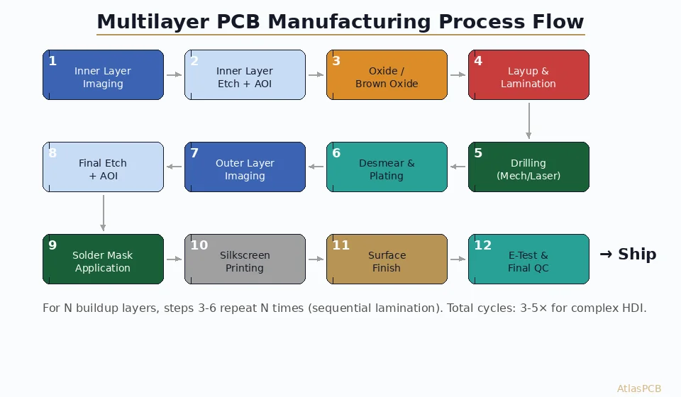
Manufacturing a multilayer PCB is fundamentally different from making a simple two-sided board. Each added layer introduces complexity in material handling, alignment, drilling, and quality control. This guide walks through the complete manufacturing process for multilayer PCBs, from 8-layer designs through 40+ layer constructions, explaining the critical steps and the engineering behind them.
Process Overview

The multilayer PCB manufacturing process consists of these major stages:
- Design data preparation (CAM)
- Inner layer fabrication
- Layer stack-up and lamination
- Drilling
- Plating (PTH — Plated Through Hole)
- Outer layer imaging and etching
- Solder mask application
- Surface finish
- Routing and profiling
- Electrical testing
- Final inspection and packaging
Let’s examine each stage in detail.
Stage 1: Design Data Preparation (CAM)
Before any physical manufacturing begins, the CAM (Computer-Aided Manufacturing) department processes the customer’s Gerber/ODB++ data:
- Design Rule Check (DRC): Verify minimum trace width, spacing, annular ring, and drill-to-copper clearance meet manufacturing capabilities
- Panelization: Arrange multiple boards on a manufacturing panel (typically 18” × 24” or 21” × 24”) with tooling borders, fiducials, registration targets, and test coupons
- Scaling compensation: Apply X and Y scaling factors to inner layer artwork to compensate for material movement during lamination. Typical scaling: 0.5–3.0 mils per 10 inches, dependent on material, layer position, and copper distribution
- Drill file optimization: Merge drill files, add tooling holes, optimize drill sequence
Stage 2: Inner Layer Fabrication
Each inner layer starts as a copper-clad laminate (core) — a sheet of cured resin/glass composite with copper foil bonded to both sides.
2.1 Surface Preparation
The copper surface is chemically cleaned and micro-roughened (pumice scrub or chemical micro-etch) to promote photoresist adhesion. Target roughness: Ra 0.3–0.5 µm.
2.2 Photoresist Lamination
Dry film photoresist (typically 25–50 µm thick) is laminated onto both sides of the core using hot rollers at 100–110°C and 3–5 bar pressure.
2.3 Exposure (Imaging)
The circuit pattern is transferred to the photoresist using one of two methods:
- Contact printing: Phototool (film) placed in direct contact with the panel; UV light exposes through the artwork. Resolution: ≥3/3 mil (75/75 µm) line/space.
- Laser Direct Imaging (LDI): A laser writes the pattern directly onto the photoresist without a phototool. Resolution: ≥2/2 mil (50/50 µm) with improved accuracy and repeatability. LDI is standard for high layer count boards.
2.4 Development
The exposed panel is developed in a sodium carbonate solution (1–1.5% Na₂CO₃) which removes the unexposed photoresist (for negative-acting resist), revealing the copper to be etched.
2.5 Etching
The exposed copper is dissolved using an etchant:
- Cupric chloride (CuCl₂): Most common for inner layers, with pH and ORP control for consistent etch rate
- Ammoniacal etchant: Used for thicker copper (≥2 oz) due to less undercut
Etch factor (ratio of vertical etch to lateral undercut) typically ranges from 2:1 to 4:1, depending on copper thickness and etchant chemistry.
2.6 Resist Stripping
The remaining photoresist is stripped in a sodium hydroxide (NaOH) solution, leaving the finished copper pattern.
2.7 Automated Optical Inspection (AOI)
Every inner layer is inspected by AOI systems that compare the etched pattern against the CAM data. Defects detected include:
- Opens (broken traces)
- Shorts (copper bridges)
- Reduced trace width
- Reduced spacing
- Missing features
Critical point: Inner layer defects cannot be repaired after lamination. AOI is the last chance to reject defective inner layers before they are buried in the stackup. For high layer count boards (20+), this is especially important — a single defective inner layer means the entire board is scrap.
2.8 Oxide Treatment (Brown Oxide / Black Oxide)
After AOI pass, the inner layers receive an oxide treatment to promote adhesion to the prepreg resin during lamination:
- Brown oxide (alternative oxide): Creates a micro-rough copper oxide layer. Most common modern process.
- Black oxide: Traditional process, largely replaced by brown oxide.
- Organic adhesion promoter: Chemical treatment that creates an organic bonding layer. Used for sequential lamination and fine-line processes.
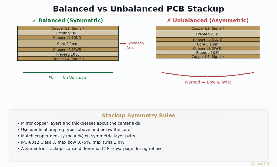
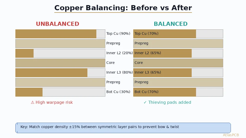
Stage 3: Layer Stack-Up and Lamination
3.1 Book Building (Lay-Up)
The stack-up is assembled in a clean room environment:
- Bottom copper foil (if outermost layer)
- Prepreg sheet(s) — uncured resin-impregnated glass fabric
- Inner layer core — positioned using registration pins or targets
- Prepreg sheet(s)
- Next inner layer core
- (Repeat for all layers)
- Prepreg sheet(s)
- Top copper foil
Registration methods:
- Pin lamination: Tooling holes in each layer fit over steel pins in the press fixture. Accuracy: ±50–75 µm.
- Mass lamination with X-ray targets: Layers are aligned using internal registration targets verified by X-ray. Accuracy: ±25–50 µm. Preferred for ≥16 layers.
3.2 Lamination Press
The assembled book is placed in a hydraulic lamination press:
| Parameter | Standard FR-4 | High-Tg FR-4 | Polyimide |
|---|---|---|---|
| Temperature | 175–185°C | 190–210°C | 230–250°C |
| Pressure | 250–350 psi | 300–400 psi | 350–450 psi |
| Ramp rate | 2–4°C/min | 2–3°C/min | 1–2°C/min |
| Dwell time | 60–90 min | 90–120 min | 120–180 min |
| Cool-down | Controlled, ~2°C/min | Controlled, ~2°C/min | Controlled, ~1°C/min |
The prepreg resin melts, flows to fill gaps around inner layer copper features, then cures (cross-links) to form a solid bond. This is an irreversible chemical process.
Critical parameters:
- Resin flow: Excessive flow causes dielectric thickness variation; insufficient flow leaves voids
- Temperature uniformity: ±2°C across the panel to prevent localized under-cure or over-cure
- Pressure uniformity: Must be even to prevent thickness variation and delamination
- Vacuum: Most modern presses use vacuum-assisted lamination (VAL) to remove trapped air and volatiles
3.3 Post-Lamination Processing
After cool-down:
- X-ray drill targeting: X-ray machines locate inner layer targets and drill precision tooling holes for subsequent drilling and routing operations
- Trim: Remove excess material from panel edges
- Thickness measurement: Verify total board thickness meets specification (typically ±10%)
Stage 4: Drilling
4.1 Mechanical Drilling
High-speed CNC drill machines create through-holes and non-plated holes:
| Parameter | Standard | High-Precision |
|---|---|---|
| Drill speed | 150,000–200,000 RPM | 200,000–300,000 RPM |
| Feed rate | 1–3 m/min | 0.5–1.5 m/min |
| Hit count per drill bit | 2,000–3,000 (standard), 500–1,000 (small drill) | 500–1,000 |
| Position accuracy | ±25 µm | ±15 µm |
| Minimum drill diameter | 0.15 mm (6 mil) | 0.10 mm (4 mil) |
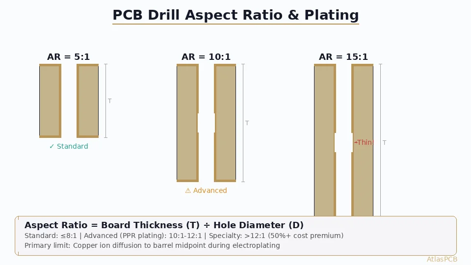
| Maximum aspect ratio | 10:1 (standard), 12:1–15:1 (advanced) | 15:1–20:1 |
Stack height: Multiple panels are stacked (typically 2–4 panels for standard boards, 1 panel for high-precision or thick boards) with entry material (aluminum) on top and backup material (phenolic or wood composite) below.
Drill bit materials:
- Carbide (WC-Co): Standard for diameters ≥0.15 mm
- Diamond-coated carbide: For abrasive materials (ceramic-filled PTFE, polyimide)
4.2 Laser Drilling (for HDI)
UV or CO₂ lasers create microvias in buildup layers:
- CO₂ laser: 9.4 µm wavelength, drills dielectric but not copper (requires conformal mask or copper window). Typical via: 75–150 µm diameter.
- UV laser (Nd:YAG, 355 nm): Drills both copper and dielectric. Smaller vias (25–75 µm) possible. Slower than CO₂.
4.3 Back-Drilling
For high-speed designs, controlled-depth drilling removes unused via stubs:
- Depth accuracy: ±0.1 mm (typical), ±0.05 mm (best-in-class)
- Back-drill diameter: Signal via diameter + 0.2 mm (typically)
- Target residual stub: 0.1–0.2 mm
Stage 5: Plating (PTH)
5.1 Desmear
After drilling, resin smear on the hole walls must be removed to ensure reliable copper-to-copper connection:
- Permanganate desmear: KMnO₄ solution dissolves resin smear. Standard for FR-4.
- Plasma desmear: CF₄/O₂ plasma etches resin in a vacuum chamber. Preferred for PTFE, polyimide, and HDI microvias.
5.2 Electroless Copper (Chemical Deposition)
A thin copper seed layer (0.3–0.8 µm) is deposited on the hole walls through an autocatalytic chemical reaction. This layer makes the non-conductive hole walls electrically conductive for subsequent electroplating.
Process sequence:
- Cleaner/conditioner
- Micro-etch (prepare existing copper surface)
- Pre-catalyst (pre-dip)
- Catalyst (Pd/Sn colloidal activation)
- Accelerator (removes Sn, exposes Pd nuclei)
- Electroless copper bath (Cu²⁺ + HCHO → Cu⁰)
5.3 Electrolytic Copper Plating
Panel or pattern plating builds up copper to the required thickness (typically 20–25 µm or 0.7–1.0 mil in the hole barrel):
| Parameter | Panel Plating | Pattern Plating |
|---|---|---|
| Copper coverage | Entire panel surface | Only exposed pad/trace areas |
| Acid copper bath | DC plating, 15–25 ASF | DC or pulse plating, 15–30 ASF |
| Throwing power | Critical for high aspect ratio | Less critical |
| Hole wall thickness | 20–25 µm minimum | 20–25 µm minimum |
| Surface copper added | 20–30 µm | 20–30 µm (on pads only) |
For high aspect ratio holes (>10:1), pulse plating or periodic-pulse-reverse (PPR) plating improves copper distribution in the hole barrel.
Stage 6: Outer Layer Imaging and Etching
The outer layer circuit pattern is formed using either print-and-etch or pattern plating, depending on the facility:
Pattern Plating Process (Most Common for Multilayer)
- Apply photoresist to panel
- Expose circuit pattern (LDI or contact print)
- Develop photoresist
- Electroplate copper (25 µm) then tin or tin-lead etch resist (3–8 µm) on exposed copper areas
- Strip photoresist
- Etch unprotected copper (ammoniacal or cupric chloride)
- Strip tin etch resist
Print-and-Etch Process
- Apply photoresist
- Expose, develop
- Etch
- Strip resist
Stage 7: Solder Mask Application
Liquid photoimageable solder mask (LPSM) is applied to protect the board surface:
- Screen print or curtain coat: Apply solder mask ink to panel
- Tack dry: Partial cure to remove solvent (75–80°C, 20–30 min)
- Expose: UV exposure through phototool or LDI to define pad openings
- Develop: Sodium carbonate solution removes unexposed mask
- Final cure: Thermal cure (150°C, 60 min) to fully cross-link the mask
Color options: Green (standard, best resolution), black, white, blue, red, matte green, matte black. Green solder mask provides the best imaging resolution due to optimal UV absorption characteristics.
Stage 8: Surface Finish
The exposed copper pads receive a surface finish to prevent oxidation and ensure solderability. For a comprehensive comparison of surface finish options, see our [PCB surface finish comparison guide]/blog/pcb-surface-finish-comparison-2026/).
Common finishes: HASL, ENIG, ENEPIG, OSP, immersion silver, immersion tin.
Stage 9: Routing and Profiling
Individual boards are separated from the manufacturing panel:
- CNC routing: Diamond-coated carbide router bits cut the board outline at 24,000–36,000 RPM
- V-scoring: V-shaped groove cut along straight separation lines for panelized assemblies
- Tab routing: Boards connected by breakaway tabs
Stage 10: Electrical Testing
Every production board is electrically tested:
- Flying probe test: Two or more moving probes test continuity (opens) and isolation (shorts) against the netlist. Best for prototypes and low-volume. Speed: 10–30 points/second per probe.
- Bed-of-nails (fixture) test: Custom test fixture with spring-loaded pins for each net. Best for high-volume production. Speed: entire board tested in seconds.
Test parameters per IPC-9252:
- Continuity threshold: <50 Ω (typically <10 Ω for through-holes)
- Isolation threshold: >2 MΩ at 100–250V DC (standard), >10 MΩ for high-reliability
Stage 11: Final Inspection and Packaging
- Visual inspection: Per IPC-A-600 (acceptability of printed boards)
- Dimensional measurement: Board outline, hole locations, feature positions
- Microsection: Destructive cross-section analysis of test coupons verifying plating thickness, dielectric thickness, copper distribution, and hole wall quality
- Impedance testing: TDR measurement of impedance test coupons
- Packaging: Vacuum-sealed bags with desiccant, per IPC-1601
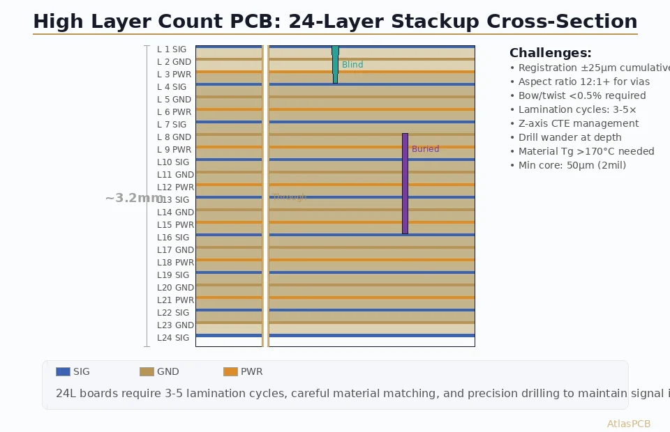
Challenges Specific to High Layer Counts (20+ Layers)
Registration Accuracy
With 20+ layers, maintaining registration across all layers is the primary challenge. Cumulative tolerance stack-up can exceed allowable limits. Solutions:
- Mass lamination with X-ray alignment (±25 µm)
- Sequential lamination for critical layers
- CTE-matched materials to minimize thermal movement during lamination
Aspect Ratio
A 40-layer board at 6.0 mm thickness with 0.3 mm vias has an aspect ratio of 20:1—at or beyond the limits of standard plating. Solutions:
- Pulse/PPR plating for improved throwing power
- Larger drill diameters (design trade-off: less routing area)
- Blind/buried vias to avoid single high-aspect-ratio through-holes
Thermal Management
High layer count boards absorb more heat during lamination and soldering. With more copper layers acting as heat sinks, achieving uniform temperature for reflow soldering requires careful profiling.
Cost Implications
Manufacturing cost increases non-linearly with layer count:
| Layer Count | Relative Cost | Typical Lead Time |
|---|---|---|
| 4 layers | 1× | 5–7 days |
| 8 layers | 1.5–2× | 7–10 days |
| 16 layers | 3–4× | 10–15 days |
| 24 layers | 5–8× | 15–20 days |
| 32+ layers | 8–15× | 20–30 days |
Quality Standards
Multilayer PCB manufacturing is governed by several IPC standards:
- IPC-6012: Qualification and Performance Specification for Rigid Printed Boards
- IPC-A-600: Acceptability of Printed Boards (visual inspection criteria)
- IPC-2221/2222: Design Standards for Rigid PCBs
- IPC-4101: Specification for Base Materials (laminate and prepreg)
- IPC-9252: Electrical Testing Requirements
- IPC-TM-650: Test Methods Manual
At Atlas PCB, our multilayer PCB manufacturing supports up to 68 layers with IPC-6012 Class 3 certification. For a stackup review and manufacturing quotation, request a quote.
Conclusion
Multilayer PCB manufacturing is a sophisticated process where each stage must be precisely controlled. From inner layer imaging accuracy to lamination temperature profiles to drill precision, the cumulative effect of all process steps determines the final board quality. Understanding this process helps designers make informed decisions about layer count, materials, via structures, and design rules.
For further reading, explore our guides on [multilayer stackup design]/blog/multilayer-pcb-stackup-design-guide/), [high layer count challenges]/blog/high-layer-count-pcb-challenges/), and [HDI PCB technology]/blog/hdi-pcb-technology/).
Further Reading
- [HDI PCB Design Guide: Stackup Rules, Via Structures & DFM Checklist]/blog/hdi-pcb-design-guide/)
- [PCB Sequential Lamination: Process, Design Rules, and When You Need It]/blog/pcb-sequential-lamination/)
- [High-Multilayer FR4 vs Standard FR4: When to Upgrade Material Grade]/blog/high-multilayer-fr4-vs-standard-fr4/)
- [PCB Manufacturing Process: 15 Steps from Gerber to Finished Board]/blog/pcb-manufacturing-process-15-steps/)
- [ENEPIG vs ENIG: Which PCB Surface Finish for Your Design?]/blog/enepig-vs-enig/)
About AtlasPCB — We specialize in complex PCB manufacturing for HDI, RF, and high-reliability applications. Explore our multilayer PCB fabrication up to 30 layers, or get an full PCB manufacturing capabilities . Every order includes free engineering review. Get your quote.
Reviewed by AtlasPCB Engineering Team — IPC-certified manufacturing specialists with 15+ years of production experience in HDI, RF, and high-reliability PCB fabrication. Content based on factory floor data and real customer design reviews.
- multilayer PCB
- manufacturing
- lamination
- drilling
- plating
- IPC-6012