· AtlasPCB Engineering · Engineering · 9 min read
PCB Surface Finish Comparison 2026: HASL vs ENIG vs ENEPIG vs OSP vs Immersion Silver
A comprehensive 2026 comparison of PCB surface finishes—HASL, lead-free HASL, ENIG, ENEPIG, OSP, immersion silver, and immersion tin. Covers solderability, shelf life, cost, wire bonding compatibility, and application-specific recommendations.

Selecting the right surface finish is one of the most impactful decisions in PCB fabrication. The surface finish protects exposed copper pads from oxidation, ensures reliable soldering during assembly, and can affect signal performance, wire bonding capability, and long-term reliability. This guide provides an updated 2026 comparison of the seven most common PCB surface finishes.
Why Surface Finish Matters
Bare copper oxidizes rapidly when exposed to air. Within hours, a thin oxide layer forms that degrades solderability. Within weeks, the oxide can become thick enough to prevent reliable solder wetting entirely. Surface finishes provide a protective barrier that maintains solderability through storage, handling, and assembly.
Beyond basic protection, the choice of surface finish affects:
- Solderability: How well solder wets and bonds to the pad
- Planarity: Surface flatness, critical for fine-pitch components (≤0.4mm BGA pitch)
- Shelf life: How long the PCB remains solderable in storage
- Wire bonding: Compatibility with gold and aluminum wire bonding
- High-frequency performance: Signal loss contribution at RF frequencies
- Contact resistance: For connectors, switches, and test points
- Cost: Direct impact on PCB fabrication price
- Environmental compliance: RoHS and REACH requirements
Surface Finish Overview
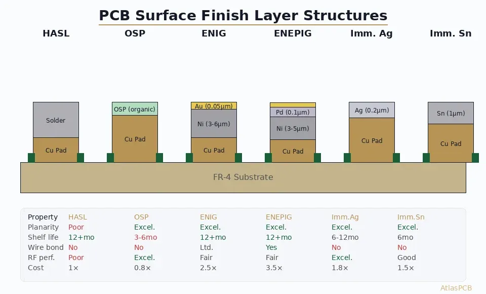
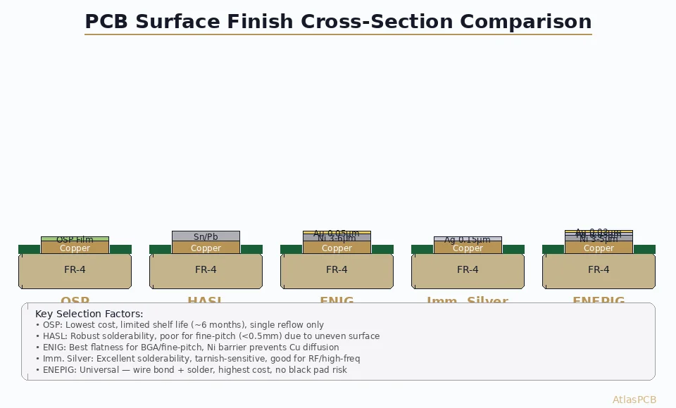
1. HASL (Hot Air Solder Leveling)
HASL is the traditional surface finish: the board is dipped in molten solder (typically 63/37 Sn/Pb or lead-free SAC305) and excess solder is removed by hot air knives.
Advantages:
- Excellent solderability and solder joint reliability
- Long shelf life (12+ months)
- Low cost
- Reworkable (multiple reflow cycles)
- Robust — very forgiving in assembly
Disadvantages:
- Non-planar surface (solder meniscus effect) — unsuitable for fine-pitch components
- Thermal shock during application (board immersed in ~250°C solder)
- Lead-free HASL requires higher temperature (~270°C), increasing thermal stress
- Bridging risk on fine-pitch pads (<0.65mm)
Best for: Through-hole heavy designs, prototypes, low-cost consumer electronics, designs with no fine-pitch components.
2. OSP (Organic Solderability Preservative)
OSP applies a thin organic compound (typically substituted benzimidazole) over bare copper to prevent oxidation. The coating is transparent and extremely thin (0.2–0.5 µm).
Advantages:
- Lowest cost surface finish
- Excellent pad planarity (copper-flat)
- Simple, environmentally friendly process
- Negligible impact on high-frequency performance (solder joint directly on copper)
- RoHS compliant
Disadvantages:
- Short shelf life (3–6 months in controlled storage)
- Degrades with each reflow cycle (typically good for 2–3 reflows maximum)
- Not suitable for press-fit connectors or contact applications
- Difficult to inspect visually (transparent on copper)
- Sensitive to handling (fingerprints can cause defects)
Best for: High-volume consumer electronics, single-reflow assemblies, cost-sensitive designs with short storage requirements.
3. ENIG (Electroless Nickel Immersion Gold)
ENIG deposits a nickel barrier layer (3–6 µm) over copper, followed by a thin immersion gold layer (0.05–0.1 µm, or 1–2 µin). The gold protects the nickel from oxidation; during soldering, the gold dissolves into the solder and the joint forms on the nickel.
Advantages:
- Excellent planarity — suitable for fine-pitch BGA (0.4mm and below)
- Long shelf life (12+ months)
- Good solderability
- Suitable for gold wire bonding (limited)
- Good contact surface for connectors and keypads
- Multiple reflow compatible
Disadvantages:
- Black pad risk: Hyper-corrosion of the nickel layer during immersion gold deposition can cause brittle, unreliable solder joints. This is the primary failure mode of ENIG.
- Higher cost than HASL or OSP
- Nickel layer is ferromagnetic — increases insertion loss at RF frequencies
- Nickel-tin intermetallic formation can reduce joint reliability over time
Best for: Fine-pitch BGA and QFN designs, mixed SMT/through-hole assemblies, boards requiring long storage life, connectors with sliding contact.
4. ENEPIG (Electroless Nickel Electroless Palladium Immersion Gold)
ENEPIG adds an electroless palladium layer between the nickel and gold. The typical stack is: Cu → Ni (3–5 µm) → Pd (0.05–0.3 µm) → Au (0.03–0.05 µm).
Advantages:
- Eliminates black pad risk (palladium barrier prevents nickel corrosion during gold deposition)
- Supports both gold AND aluminum wire bonding
- Excellent solderability — palladium dissolves in solder, forming reliable Sn-Pd-Ni intermetallic
- Long shelf life (12+ months)
- Good planarity
- Universal finish — works for SMT, wire bonding, press-fit, and contact applications
Disadvantages:
- Highest cost among standard finishes (palladium price volatility)
- Process complexity (four chemical baths)
- Palladium price sensitivity — Pd was ~$1,000/oz in early 2026
- Nickel layer still present (RF insertion loss concern remains)
Best for: Mixed-technology boards (SMT + wire bonding), automotive/aerospace high-reliability designs, boards with both fine-pitch assembly and connector contact pads.
For a detailed ENIG vs ENEPIG comparison, see our dedicated [ENEPIG vs ENIG guide]/blog/enepig-vs-enig/).
5. Immersion Silver (IAg)
Immersion silver deposits a thin layer of silver (0.15–0.4 µm) directly on copper through a displacement reaction.
Advantages:
- Excellent planarity
- Best high-frequency performance — minimal signal loss contribution
- Good solderability (silver wets well)
- Lower cost than ENIG/ENEPIG
- No nickel layer — no ferromagnetic loss
- Fine-pitch capable
Disadvantages:
- Tarnishing — silver sulfide formation in sulfur-containing environments (brown/black discoloration)
- Moderate shelf life (6–12 months with proper packaging)
- Sensitive to handling and environment (requires sulfur-free packaging)
- Micro-voiding in solder joints reported with some flux chemistries
- Electromigration potential in high-humidity environments
- Not suitable for wire bonding
Best for: High-frequency/RF applications, cost-sensitive fine-pitch designs, automotive radar modules (24/77 GHz).
6. Immersion Tin (ISn)
Immersion tin deposits a tin layer (0.8–1.2 µm) on copper.
Advantages:
- Good planarity
- Good solderability
- Moderate cost
- Compatible with press-fit connectors
- No nickel layer
Disadvantages:
- Tin whisker risk (mitigated by process control but not eliminated)
- Short shelf life (6 months typical)
- Handling sensitivity
- Not suitable for multiple reflow cycles
- Copper-tin intermetallic growth reduces shelf life
Best for: Press-fit connector applications, lead-free solder compatibility, designs assembled shortly after fabrication.
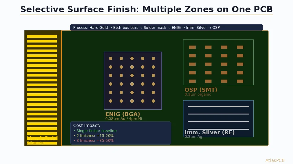
7. Hard Electrolytic Gold
For completeness, hard electrolytic gold (1–2.5 µm Au over 2.5–5 µm Ni) is used for edge connectors, contact switches, and applications requiring wear resistance. It is applied selectively (gold fingers) and is not a full-board surface finish.
Comprehensive Comparison Table
| Property | HASL (LF) | OSP | ENIG | ENEPIG | Imm. Silver | Imm. Tin |
|---|---|---|---|---|---|---|
| Thickness | 1–25 µm | 0.2–0.5 µm | Ni: 3–6 µm, Au: 0.05–0.1 µm | Ni: 3–5 µm, Pd: 0.05–0.3 µm, Au: 0.03–0.05 µm | 0.15–0.4 µm | 0.8–1.2 µm |
| Planarity | Poor | Excellent | Excellent | Excellent | Excellent | Excellent |
| Shelf life | 12+ months | 3–6 months | 12+ months | 12+ months | 6–12 months | 6 months |
| Fine-pitch (<0.5mm) | No | Yes | Yes | Yes | Yes | Yes |
| Reflow cycles | 4+ | 2–3 | 3–4 | 3–4 | 3–4 | 2–3 |
| Au wire bonding | No | No | Limited | Yes | No | No |
| Al wire bonding | No | No | No | Yes | No | No |
| RF performance | Poor (uneven surface) | Excellent | Fair (Ni loss) | Fair (Ni loss) | Excellent | Good |
| Press-fit | Fair | Poor | Fair | Good | Fair | Good |
| Contact/switch | Poor | Poor | Good | Good | Fair | Poor |
| Black pad risk | None | None | Yes | No | None | None |
| Relative cost | 1× | 0.8× | 2.5× | 3.5× | 1.8× | 1.5× |
| RoHS | LF only | Yes | Yes | Yes | Yes | Yes |
| IPC J-STD-003 | Yes | Yes | Yes | Yes | Yes | Yes |
Application-Specific Recommendations
Consumer Electronics (Smartphones, Wearables)
Recommended: OSP or ENIG
For high-volume consumer electronics with controlled supply chains and short storage times, OSP provides the best cost-to-performance ratio. Fine-pitch BGAs and QFNs are easily assembled on OSP pads. For designs requiring longer shelf life or multiple reflow cycles, upgrade to ENIG.
Automotive Electronics
Recommended: ENEPIG or ENIG
Automotive applications demand high reliability and long product life. ENEPIG is increasingly the automotive standard due to its wire bonding compatibility (required for some power module designs) and elimination of black pad risk. ENIG is acceptable for non-wire-bonded applications.
Aerospace and Defense
Recommended: ENEPIG
Aerospace applications often combine SMT assembly, wire bonding, and connector contacts on the same board. ENEPIG’s universal compatibility makes it the default choice. Long storage requirements (boards may sit in inventory for years) further favor ENEPIG or ENIG over OSP.
RF/Microwave and 5G
Recommended: Immersion Silver or OSP
For applications above 1 GHz, the nickel layer in ENIG/ENEPIG degrades performance measurably. At 10 GHz, ENIG adds approximately 0.02–0.05 dB/cm insertion loss compared to bare copper. Immersion silver is the preferred RF finish. OSP is acceptable if assembly occurs promptly after fabrication.
Medical Devices
Recommended: ENIG or ENEPIG
Medical devices require long shelf life, reliable solder joints, and often gold wire bonding for sensor assemblies. ENEPIG is ideal for mixed-technology medical boards.
Prototyping and Quick-Turn
Recommended: HASL (lead-free) or ENIG
For prototypes where speed matters, HASL is widely available with the shortest processing time. ENIG is recommended if the prototype includes fine-pitch components that require flat pads.
Black Pad: Understanding and Preventing ENIG’s Primary Failure Mode
Black pad is a corrosion-induced defect specific to ENIG where the immersion gold deposition process attacks the nickel surface, creating a phosphorus-rich, gold-depleted nickel layer. This layer appears black or dark gray under the gold and results in:
- Brittle solder joints that fracture at the pad interface
- Reduced pull/shear strength (50–80% reduction)
- Field failures under thermal cycling or mechanical stress
Causes
- Excessive gold deposition time or temperature — extends the galvanic attack on nickel
- Nickel bath chemistry imbalance — low phosphorus content (should be 7–9 wt%) or contamination
- Pad geometry — small pads and narrow traces are more susceptible
- Bath age — older ENIG baths produce more variable deposits
Prevention
- Process control: Maintain nickel phosphorus content at 7–9 wt%, gold thickness at 0.05–0.08 µm
- Supplier qualification: Audit ENIG process regularly per IPC-4552 Rev B
- Switch to ENEPIG: The palladium layer fundamentally prevents the corrosion mechanism
- Incoming inspection: Cross-section and measure nickel/gold thickness; inspect for corrosion indicators
Surface Finish and Solder Joint Reliability
The surface finish affects solder joint metallurgy:
HASL
Solder-on-solder joint. Excellent reliability. No intermetallic concerns beyond standard Sn-Cu formation.
OSP
Solder directly on copper. Forms Cu₃Sn and Cu₆Sn₅ intermetallic — well-characterized, reliable.
ENIG
Gold dissolves into solder (Au-Sn intermetallic forms if gold is too thick — keep <0.1 µm). Joint forms on Ni₃Sn₄ intermetallic. Generally reliable unless black pad occurs.
ENEPIG
Palladium and gold dissolve into solder. Joint forms primarily on Ni₃Sn₄ with minor Pd-Sn phases. More reliable than ENIG due to absence of black pad.
Immersion Silver
Silver dissolves into solder. Joint forms on Cu-Sn intermetallic (same as OSP). Potential micro-void formation at the Ag-Sn interface — use appropriate flux chemistry.
Cost Analysis (2026)
Surface finish cost is typically 2–8% of total PCB fabrication cost. For a standard 6-layer, 100×100mm board:
| Finish | Added cost per board (approx.) | % of total PCB cost |
|---|---|---|
| OSP | $0.10–0.20 | ~2% |
| HASL (lead-free) | $0.15–0.30 | ~3% |
| Immersion tin | $0.20–0.40 | ~3% |
| Immersion silver | $0.30–0.50 | ~4% |
| ENIG | $0.50–1.00 | ~5% |
| ENEPIG | $0.80–1.50 | ~7% |
For high-volume production (>10,000 boards), negotiate surface finish pricing with your fabricator. At Atlas PCB, we offer competitive pricing across all standard surface finishes with volume discounts.
How to Specify Surface Finish
When ordering PCBs, specify the following in your fabrication notes:
- Finish type: e.g., “ENIG per IPC-4552 Rev B”
- Thickness requirements:
- ENIG: Ni 3–6 µm, Au 0.05–0.1 µm (or specify “soft gold” vs “hard gold” for selective plating)
- ENEPIG: Ni 3–5 µm, Pd 0.05–0.15 µm, Au 0.03–0.05 µm
- Applicable standard: IPC-4552 (ENIG), IPC-4556 (ENEPIG), IPC-4553 (immersion silver), IPC-4554 (immersion tin)
- Selective finish: If using different finishes on different areas (e.g., ENIG for pads, hard gold for edge connectors), clearly mark areas on drawings
- Acceptance criteria: IPC-6012 class (Class 2 or Class 3)
Conclusion
No single surface finish is best for all applications. The choice depends on your design’s specific requirements: component pitch, frequency, wire bonding needs, storage duration, reliability class, and budget. As a general guide for 2026:
- High volume, low cost: OSP
- General purpose: ENIG
- High reliability / wire bonding: ENEPIG
- RF/microwave: Immersion silver
- Prototyping: Lead-free HASL
At Atlas PCB, we process all major surface finishes in-house and can advise on the optimal choice for your specific application. Our [surface finish selection guide]/blog/pcb-surface-finish-guide/) provides additional detail, or contact us for a quote with finish-specific pricing.
Further Reading
- [PCB Surface Finish Guide: HASL, ENIG, OSP and More Compared]/blog/pcb-surface-finish-guide/)
About AtlasPCB — We specialize in complex PCB manufacturing for HDI, RF, and high-reliability applications. Explore our RF and high-frequency PCB services, or get an full PCB manufacturing capabilities . Every order includes free engineering review. Get your quote.
Reviewed by AtlasPCB Engineering Team — IPC-certified manufacturing specialists with 15+ years of production experience in HDI, RF, and high-reliability PCB fabrication. Content based on factory floor data and real customer design reviews.
- surface finish
- ENIG
- ENEPIG
- HASL
- OSP
- immersion silver