· AtlasPCB Engineering · Engineering · 11 min read
High Layer Count PCB Challenges: Designing and Manufacturing 20 to 68 Layer Boards
An in-depth analysis of the engineering challenges in high layer count PCB design and manufacturing—from registration accuracy and aspect ratio limits to thermal management, material selection, and cost optimization for 20 to 68 layer boards.
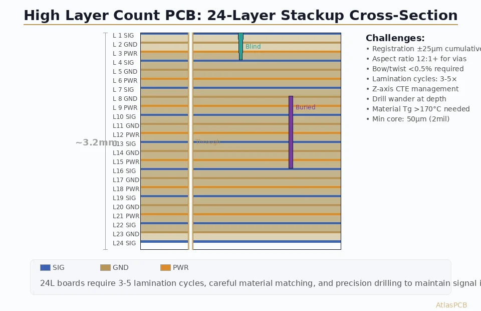
High layer count PCBs—boards with 20 to 68 or more copper layers—are essential in networking, telecommunications, data center computing, aerospace, and defense applications. These boards pack thousands of signal nets into a single substrate, but they push manufacturing technology to its limits. This article examines the key challenges and engineering solutions for ultra-high layer count PCB design and manufacturing.
Why High Layer Counts?

The demand for 20+ layer boards comes from several converging trends:
- High-pin-count devices: Modern FPGAs (Intel Agilex, AMD Versal) and ASICs can have 3,000–5,000+ I/O pins. Routing all these signals through the package breakout zone requires many routing layers.
- Power distribution: High-performance processors require multiple power rails with tight voltage regulation. Each power domain often needs dedicated power and ground plane pairs.
- Signal integrity: Maintaining controlled impedance and minimizing crosstalk requires dedicated ground reference planes. The “every signal layer gets a reference plane” rule doubles the required layer count.
- High-speed serial links: Interfaces like PCIe Gen 5/6, 100G/400G Ethernet, and DDR5 require careful routing on impedance-controlled stripline layers with adequate spacing.
- Form factor constraints: System density requirements limit board area, forcing more routing into the Z-axis (additional layers).
Typical Applications by Layer Count
| Layer Count | Application Examples |
|---|---|
| 20–24 | High-end networking switches, server motherboards |
| 24–32 | Data center switches, 5G base station processing cards |
| 32–40 | High-performance computing, FPGA prototyping boards |
| 40–52 | Military radar processors, advanced telecom line cards |
| 52–68 | Semiconductor test equipment (ATE), extreme-density computing |
Challenge 1: Layer-to-Layer Registration
The Problem
Each inner layer core is fabricated independently. During lamination, these layers must align with each other to within tight tolerances so that drilled holes intersect their target pads on every layer.
For a via with a 0.3 mm drill and a 0.55 mm pad (annular ring = 0.125 mm), the maximum tolerable misregistration between any two layers is 0.125 mm. This seems generous—until you consider that with 40 layers, you need every layer pair to meet this requirement simultaneously.
Registration Error Sources
| Source | Typical Magnitude | Notes |
|---|---|---|
| Artwork accuracy | ±5–10 µm | LDI is better than contact print |
| Material dimensional stability | ±25–75 µm | Varies with material, copper balance |
| Lamination movement | ±15–25 µm | Per lamination cycle |
| Drilling accuracy | ±15–25 µm | CNC drill registration |
| Temperature variation in press | ±10–20 µm | Non-uniform heating causes differential movement |
Total budget (RSS): For a 40-layer board with mass lamination: √(10² + 50² + 20² + 20² + 15²) ≈ 62 µm (RSS)
This leaves approximately 63 µm margin for a 125 µm annular ring budget—tight but achievable.
Solutions
- X-ray alignment: Locate inner layer fiducials with X-ray systems after lamination. Use these for drill targeting. Accuracy: ±10–15 µm.
- Scaling compensation: Pre-scale inner layer artwork based on historical lamination movement data. Different layers may need different scaling factors based on copper density.
- CTE-matched materials: Use materials with consistent X/Y CTE across layers (e.g., Isola 370HR, Panasonic Megtron series).
- Symmetrical copper distribution: Balance copper coverage on each layer pair to minimize differential shrinkage during lamination.
- Sequential lamination: For the most critical designs, laminate in sub-groups (e.g., two 20-layer sub-stacks) and drill/plate between groups.
- Larger pads: When routing density allows, increase pad diameter to provide more registration margin. A 0.65 mm pad with a 0.3 mm drill provides 0.175 mm annular ring budget.
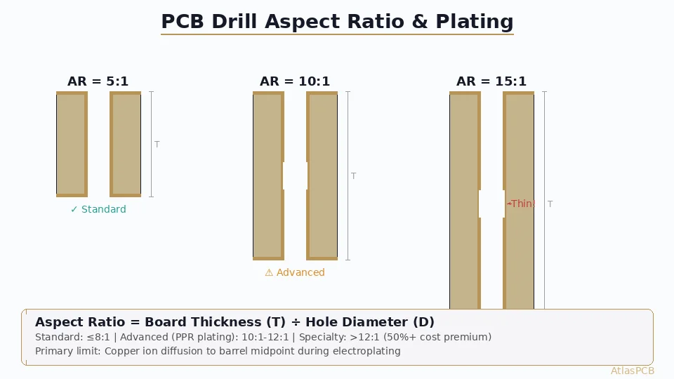
Challenge 2: Aspect Ratio and Through-Hole Plating
The Problem
Board thickness increases with layer count. A 40-layer board at 150 µm per layer pair is approximately 3.0–4.0 mm thick (including prepreg, cores, and copper). A 60-layer board can be 5.0–6.0 mm or more.
The aspect ratio (board thickness ÷ hole diameter) determines how well copper can be deposited inside the drilled hole:
| Board Thickness | Drill Diameter | Aspect Ratio | Plating Difficulty |
|---|---|---|---|
| 2.0 mm | 0.25 mm | 8:1 | Standard |
| 3.0 mm | 0.25 mm | 12:1 | Challenging |
| 4.0 mm | 0.30 mm | 13:1 | Advanced |
| 5.0 mm | 0.35 mm | 14:1 | Expert |
| 6.0 mm | 0.40 mm | 15:1 | Near limit |
At aspect ratios above 10:1, standard DC acid copper plating struggles to deposit uniform copper in the center of the hole barrel. The “throwing power” of the bath decreases, resulting in thin copper at the barrel midpoint—the weakest link for reliability.
Solutions
- Pulse plating / PPR (Periodic Pulse Reverse): Alternating forward and reverse current pulses improve copper distribution in high aspect ratio holes. Can extend practical limits to 15:1–20:1.
- Increase drill diameter: The simplest solution, but reduces routing density. For a 4.0 mm board at 12:1, minimum drill is 0.33 mm—which requires a 0.6+ mm pad.
- Blind/buried via combinations: Use HDI buildup layers with blind microvias for the outermost layers, reducing the through-hole depth to the core section only. A 40-layer board with 2+36+2 construction has through-holes penetrating only 36 layers (~4.2 mm) while the outer 2 layers per side use blind vias.
- Segmented via structures: Split a single deep through-hole into two or more overlapping blind/buried segments, each with a more manageable aspect ratio.
- Via-in-pad plating: For [via-in-pad designs]/blog/via-in-pad-design/), filled and capped vias in high aspect ratio holes require specialized plating processes.
Challenge 3: Drilling
Mechanical Drilling Limits
High layer count boards present drilling challenges beyond aspect ratio:
- Drill wander: In thick boards, the drill bit can deflect from its intended path. For a 5 mm thick board, positional accuracy at the exit side may be ±50 µm worse than at the entry side.
- Hole wall quality: Deeper holes show more smear (resin debris) on inner layer connections, requiring aggressive desmear.
- Drill bit life: Thicker boards consume more drill life per hit. Bit replacement frequency increases, raising cost.
- Stack height: Only 1–2 panels can be drilled simultaneously (vs. 3–4 for standard boards).
Solutions
- Entry/exit material optimization: Use precision aluminum entry sheets and controlled-expansion backup materials
- Reduced stack heights: Single-panel drilling for boards >3 mm thick
- Controlled feed rates: Slower feed rates improve hole wall quality in thick boards
- Drill bit selection: Step-drill geometry for high aspect ratio holes; under-cut drills for reduced smear
- Back-drilling: For high-speed signals, back-drill stub removal with controlled depth accuracy of ±0.1 mm. See our [back-drill guide]/blog/pcb-back-drill/).
Challenge 4: Thermal Management
During Lamination
A 40-layer stackup has substantial thermal mass. Achieving uniform temperature throughout the book during lamination is difficult:
- Temperature gradient: The center of a thick stackup reaches peak temperature 10–20 minutes after the surfaces. Under-cure in the center or over-cure on the outside can result.
- Resin flow: Temperature gradients cause uneven resin flow, leading to dielectric thickness variation.
- Trapped volatiles: Thicker books are more prone to moisture-related voids if not properly dried before lamination.
Solutions:
- Extended ramp rates (1–2°C/min vs. standard 3–4°C/min)
- Extended dwell times at cure temperature (120–180 min)
- Vacuum-assisted lamination to remove trapped air
- Pre-bake inner layers and prepreg (105°C, 2–4 hours) to remove moisture
During Assembly (Reflow Soldering)
High layer count boards act as massive heat sinks during reflow. The thermal profile required to reach solder liquidus (217°C for SAC305) on the surface while not overheating components is challenging:
- Longer preheat zone needed to bring the entire board to soak temperature uniformly
- Higher peak temperature may be required (245–260°C vs. standard 235–245°C)
- Extended time above liquidus (TAL) for reliable solder joints on thick boards
- Thermal damage risk to components sensitive to extended high-temperature exposure
Challenge 5: Material Selection
Dielectric Materials
High layer count boards need materials that can withstand multiple processing cycles while maintaining dimensional stability:
| Property | Requirement for High Layer Count | Why |
|---|---|---|
| Tg (Glass Transition) | ≥170°C | Multiple reflow cycles, lead-free assembly |
| Td (Decomposition) | ≥340°C | Extended high-temperature exposure during lamination |
| Z-axis CTE (< Tg) | <55 ppm/°C | Reduce barrel stress in high aspect ratio holes |
| Z-axis CTE (> Tg) | <250 ppm/°C | Reduce expansion above Tg during reflow |
| X/Y CTE | 14–17 ppm/°C | Close to copper (17 ppm/°C) for registration |
| Dk tolerance | ±3% or better | Impedance control across many layers |
| CAF resistance | High | Dense via fields increase CAF risk |
Recommended materials for 20+ layers:
- Isola 370HR: Tg 180°C, Td 340°C, excellent dimensional stability. Workhorse for networking and computing.
- Panasonic Megtron 4 (R-5775): Tg 175°C, low-loss (Df 0.005 at 1 GHz). Good for mixed high-speed and high layer count.
- Shengyi S1000-2M: Tg 170°C, cost-effective high-Tg option for 20–30 layer boards.
Copper Weight
Inner layer copper weight affects registration, etching, and impedance:
- ½ oz (17 µm): Standard for signal layers. Best fine-line capability.
- 1 oz (35 µm): Standard for power/ground planes. Higher current capacity.
- 2 oz (70 µm): Heavy power planes. Requires thicker prepreg for fill. Impacts total board thickness.
For high layer count boards, minimizing copper weight (½ oz where possible) reduces total thickness and improves aspect ratios.
Challenge 6: Cost and Lead Time
Cost Drivers
- Inner layer cores: Each layer pair requires a separate core with full imaging, etching, and AOI. Cost is roughly proportional to layer count.
- Scrap compounding: If each inner layer has a 2% defect rate, the probability of all 40 inner layers passing is 0.98²⁰ = 67%. One in three boards has at least one defective inner layer (assuming 20 cores for 40 layers). For 60 layers, yield drops to 0.98³⁰ = 55%.
- Lamination press time: A 40-layer press cycle takes 3–4 hours (vs. 1–2 hours for 8 layers). Press capacity becomes the bottleneck.
- Drilling time: More holes per board (often 20,000–50,000+), larger drill files, slower speeds for thick boards.
- Testing time: More nets to test, longer flying probe or fixture test cycles.
Cost Optimization Strategies
- Minimize layer count: Challenge every requirement. Can some signals be routed on existing layers with creative topology? Can some ground planes be shared?
- Optimize via structure: Use blind/buried vias to reduce through-hole count and aspect ratio, even if it adds HDI cost—the net savings from reduced drill diameter and improved yield may be positive.
- Standardize materials: Using one material system throughout the stackup simplifies procurement and lamination.
- Panel utilization: Larger boards reduce panel count. Consider consolidating multiple small boards onto a larger assembly panel.
- Design for manufacturability: Engage your fabricator early. At Atlas PCB, we offer free DFM review for high layer count designs, identifying cost reduction opportunities before production.
Challenge 7: Impedance Control Across Many Layers
With 20+ signal layers, maintaining consistent impedance across all layers requires:
- Dielectric thickness control: Each prepreg and core thickness must be within ±10% (or ±5% for tight impedance). With 20 dielectric layers, even small variations compound.
- Copper balance: Uneven copper distribution on adjacent layers causes prepreg resin flow variation, affecting dielectric thickness. Thieving copper (dummy copper fill) helps equalize copper density.
- Process coupons: Include impedance test coupons for each unique signal layer pair on the panel.
- Material Dk consistency: Ensure Dk is consistent across all prepreg and core materials in the stackup. Mixing materials from different manufacturers can introduce Dk discontinuities.
For detailed impedance control guidance, see our [controlled impedance PCB guide]/blog/controlled-impedance-pcb/).
Design Guidelines for High Layer Count PCBs
Stackup Planning
- Layer assignment: Dedicate ground planes adjacent to every high-speed signal layer. Use power planes only where needed.
- Symmetry: Maintain a symmetrical stackup (mirror image about the center) to prevent warpage.
- Dielectric thickness: Use thinner dielectrics (75–100 µm) where possible to reduce total thickness. Thicker dielectrics (125–200 µm) for power planes where capacitance is less critical.
Via Planning
- Through-hole vias: Reserve for power delivery and non-critical signals
- Blind vias (laser): Use for BGA breakout and outer layer routing
- Buried vias: Use for inner layer-to-inner layer connections to free up through-hole real estate
- Back-drilled vias: Essential for all high-speed signal vias (10+ Gbps)
Power Distribution
- Plane pairs: Place power and ground planes adjacent to each other for maximum decoupling capacitance
- Via sharing: Multiple power vias can share a single drill location with a larger pad
- Copper weight: Use 1 oz copper for power planes carrying >5A total current
Case Study: 48-Layer Networking Switch Board
Application: 400G Ethernet switching platform
Board dimensions: 350 × 450 mm
Total layer count: 48
Material: Isola 370HR + Megtron 4 (hybrid)
Board thickness: 5.2 mm
Minimum drill: 0.30 mm (mechanical), 0.10 mm (laser blind via)
Aspect ratio: 17:1 (maximum, for 0.30 mm vias)
Impedance: 42.5 Ω single-ended, 85 Ω differential (PCIe Gen 5)
Layer assignment:
- 20 signal layers (stripline, Megtron 4 dielectric)
- 16 ground planes
- 8 power planes
- 4 HDI layers (2+44+2 construction)
Key manufacturing decisions:
- Pulse-reverse plating for 17:1 aspect ratio through-holes
- X-ray alignment with sequential lamination for outer buildup layers
- Back-drill on all high-speed signal vias (residual stub <0.15 mm)
- ½ oz copper on all signal layers, 1 oz on power/ground
- 100% electrical testing with flying probe
- 100% cross-section verification on first articles
Conclusion
High layer count PCB design and manufacturing is a discipline where small decisions compound across dozens of layers. Registration accuracy, aspect ratio management, thermal control, and material selection are not independent challenges—they interact and constrain each other. Success requires a holistic approach and close partnership between the PCB designer and fabricator.
At Atlas PCB, we specialize in high layer count manufacturing up to 68 layers, with advanced capabilities including pulse plating for high aspect ratios, X-ray registration, and back-drilling. Contact us for a quote on your high layer count project.
For related reading, see our guides on [multilayer PCB manufacturing process]/blog/multilayer-pcb-manufacturing-process-explained/), [HDI stackup design]/blog/hdi-pcb-stackup-design-advanced/), and [stackup design]/blog/pcb-stackup-design-guide/).
Further Reading
- [HDI PCB Design Guide: Stackup Rules, Via Structures & DFM Checklist]/blog/hdi-pcb-design-guide/)
- [HDI PCB Technology: Microvias, Laser Drilling, and High-Density Design]/blog/hdi-pcb-technology/)
- [PCB Sequential Lamination: Process, Design Rules, and When You Need It]/blog/pcb-sequential-lamination/)
- [How to Design an HDI Stackup: Step-by-Step for First-Time Designers]/blog/how-to-design-hdi-stackup/)
- [Blind Via vs Buried Via: Design Rules, Cost Impact & When to Use Each]/blog/blind-via-vs-buried-via/)
About AtlasPCB — We specialize in complex PCB manufacturing for HDI, RF, and high-reliability applications. Explore our multilayer PCB fabrication up to 30 layers, or get an aluminum and metal-core PCB services . Every order includes free engineering review. Get your quote.
Reviewed by AtlasPCB Engineering Team — IPC-certified manufacturing specialists with 15+ years of production experience in HDI, RF, and high-reliability PCB fabrication. Content based on factory floor data and real customer design reviews.
- high layer count
- multilayer PCB
- registration
- aspect ratio
- thermal management