· AtlasPCB Engineering · Engineering · 12 min read
Advanced HDI PCB Stackup Design: Sequential Lamination, Any-Layer HDI, and ELIC
A deep technical guide to advanced HDI stackup architectures including sequential lamination, any-layer HDI, and Every Layer Interconnect (ELIC). Learn design rules, material selection, and manufacturing considerations for HDI Types I through III.
High Density Interconnect (HDI) technology has evolved far beyond simple blind and buried vias. As component pitches shrink below 0.5 mm and functional density increases, PCB designers must leverage advanced HDI stackup architectures—sequential lamination, any-layer HDI, and Every Layer Interconnect (ELIC)—to route complex designs successfully. This guide covers the theory, design rules, material considerations, and manufacturing realities of advanced HDI stackups.
HDI Classification: Types I, II, and III
The IPC-2226 standard defines three HDI types based on microvia and via structures:

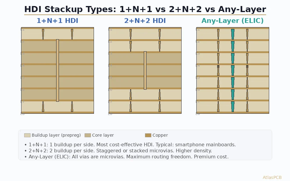
Type I — Single Microvia Layer (1+N+1)
Type I HDI has one buildup layer on each side of a conventional core. Microvias connect the outer layer to the adjacent inner layer. The core uses standard mechanical-drilled through-holes.
- Typical stackup: 1+N+1 (e.g., 1+4+1 = 6 layers)
- Microvia: Single-depth blind via, laser-drilled
- Application: Smartphones, tablets, mid-density designs
- BGA breakout: Up to 0.5 mm pitch comfortably
Type II — Stacked/Staggered Microvias (2+N+2 or higher)
Type II adds multiple buildup layers per side, with microvias that may be stacked or staggered. The core still contains mechanical through-holes.
- Typical stackup: 2+N+2, 3+N+3
- Microvia: Multi-depth, stacked with copper-filled vias or staggered
- Application: High-performance computing, networking, advanced mobile
- BGA breakout: 0.4 mm pitch feasible
Type III — Any-Layer HDI / ELIC
Type III eliminates the conventional core entirely or uses a thin core with all layers interconnected via stacked microvias. Every layer has microvia access to adjacent layers—hence “Every Layer Interconnect.”
- Typical stackup: 3+N+3 through 7+N+7 (coreless or thin-core)
- Microvia: Stacked copper-filled microvias on every layer
- Application: Leading-edge smartphones (iPhone, flagship Android), advanced AI/ML modules
- BGA breakout: 0.3 mm pitch and below
| Feature | Type I (1+N+1) | Type II (2+N+2) | Type III (ELIC) |
|---|---|---|---|
| Buildup layers per side | 1 | 2–3 | 3–7+ |
| Microvia depth | Single | Multi (stacked/staggered) | All layers |
| Through-holes in core | Yes | Yes | Optional/None |
| Min BGA pitch | 0.5 mm | 0.4 mm | 0.3 mm |
| Lamination cycles | 1 per side | 2–3 per side | 3–7+ per side |
| Relative cost | 1× | 1.5–2× | 3–8× |
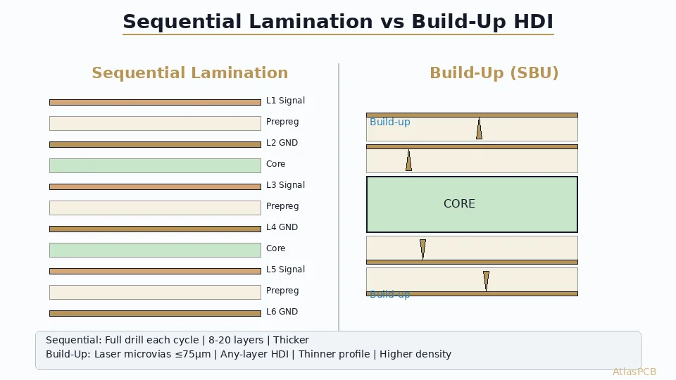
Sequential Lamination: The Manufacturing Foundation
Sequential lamination is the process that makes multi-level buildup structures possible. Unlike conventional PCBs where all layers are pressed in a single lamination cycle, sequential lamination adds layers progressively.
How Sequential Lamination Works
- Core fabrication: Start with a double-sided or multilayer core panel, fabricated using standard processes (drilling, plating, etching).
- Buildup layer addition: Apply prepreg and copper foil (or resin-coated copper, RCC) to one or both sides of the core.
- Lamination cycle: Press under heat and pressure (typically 180–200°C, 300–400 psi for standard FR-4 or 200–250°C for high-Tg materials).
- Laser drilling: Form microvias using CO₂ or UV laser. CO₂ lasers are faster for standard dielectrics; UV (Nd:YAG or excimer) lasers produce smaller, cleaner vias.
- Desmear and plating: Clean via holes (permanganate or plasma desmear) and electroplate copper to form the interconnect.
- Outer layer imaging and etching: Pattern the new copper layer.
- Repeat: For each additional buildup layer, repeat steps 2–6.
Critical Parameters in Sequential Lamination
| Parameter | Typical Range | Notes |
|---|---|---|
| Prepreg thickness | 40–100 µm | Thinner for high-density builds |
| Copper foil thickness | 12–18 µm (½ oz) | Thinner foils for fine-line capability |
| Lamination temperature | 180–250°C | Material dependent |
| Lamination pressure | 200–400 psi | Higher for void-free fill |
| Registration tolerance | ±25–50 µm per cycle | Cumulative — critical for stacked vias |
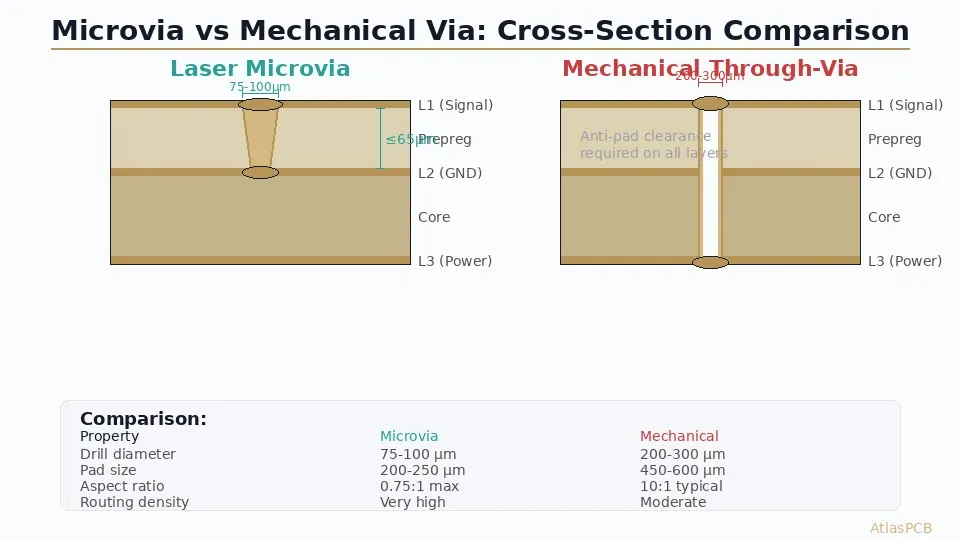
| Microvia diameter | 75–150 µm | Laser drilled |
| Microvia depth | 50–100 µm | Aspect ratio ≤0.75:1 preferred |
Registration: The Cumulative Challenge
Each sequential lamination cycle introduces registration error between the new layer and existing layers. For a 3+N+3 stackup, the outermost microvia layer has been through 3 lamination cycles relative to the core. With ±25 µm tolerance per cycle, cumulative misregistration can reach ±75 µm.
This is why stacked microvia structures demand tighter registration than staggered designs. A stacked via column where the top microvia must align precisely with vias on layers 2, 3, and 4 leaves very little room for error. Typical via pad capture requirements:
- Microvia pad: 250–350 µm diameter
- Microvia drill: 100–125 µm diameter
- Annular ring requirement: ≥50 µm (per IPC-6012 Class 3)
- Available registration budget: (Pad – Drill)/2 – Annular ring = (300–100)/2 – 50 = 50 µm
For 3 lamination cycles at ±25 µm each (RSS): √(3 × 25²) ≈ 43 µm. This is tight but achievable. For 5+ cycles, the pad must grow or tolerances must tighten, both of which impact density and cost.
Any-Layer HDI (ELIC): Design Freedom and Constraints
Any-layer HDI—often called ELIC (Every Layer Interconnect)—represents the pinnacle of HDI technology. In an ELIC stackup, every layer pair is connected by copper-filled stacked microvias, and through-holes are eliminated or minimized.
Benefits of ELIC
- Maximum routing density: Any signal can transition to any layer at any point via stacked microvias, providing unparalleled routing flexibility.
- Shorter signal paths: Signals can route on the closest available layer pair, reducing stub effects and improving signal integrity.
- Via-in-pad everywhere: Since all vias are filled and planar, via-in-pad is the default—no dog-bone fanouts needed, saving board space.
- Symmetric stackup freedom: Designers can optimize impedance on every layer pair without being constrained by through-hole keep-out areas.
- Reduced layer count: The improved routing efficiency often allows designers to achieve the same connectivity in fewer layers compared to through-hole-based designs.
Design Rules for ELIC
| Parameter | Aggressive | Standard | Conservative |
|---|---|---|---|
| Line width/space | 40/40 µm | 50/50 µm | 75/75 µm |
| Microvia diameter | 75 µm | 100 µm | 125 µm |
| Microvia pad | 200 µm | 250 µm | 300 µm |
| Via-in-pad pitch | 0.3 mm | 0.4 mm | 0.5 mm |
| Copper fill (via) | Electrolytic | Electrolytic | Electrolytic |
| Max stacked depth | 7 layers | 5 layers | 3 layers |
| Dielectric thickness | 45–60 µm | 60–80 µm | 80–100 µm |
Stacked vs. Staggered Microvias
The choice between stacked and staggered microvia arrangements is one of the most consequential decisions in HDI stackup design.
Stacked microvias align vertically across multiple layers, forming a solid copper column. Benefits include minimal signal path length, highest density, and via-in-pad compatibility. However, they require copper-filled vias (conformal copper is insufficient for reliable stacking), tighter registration, and more expensive processing.
Staggered microvias offset each via from the one below, connecting to the target net via a short trace on the intermediate layer. They are easier to manufacture, tolerate looser registration, and do not require filled vias. The trade-off is reduced density and slightly longer signal paths.
For ELIC designs targeting 0.4 mm pitch BGA or finer, stacked copper-filled microvias are essentially mandatory. For 0.5 mm pitch applications, staggered designs may be sufficient and more cost-effective.
Material Selection for Advanced HDI
Material choice profoundly impacts both the manufacturability and performance of advanced HDI stackups.
Prepreg and Core Materials
Standard FR-4 (Tg 135–170°C) is suitable for simple 1+N+1 HDI. For advanced builds with multiple lamination cycles, the material must withstand repeated thermal excursions without degradation:
- High-Tg FR-4 (Tg ≥170°C): Suitable for up to 3+N+3 with standard reliability requirements. Examples: Isola 370HR, Shengyi S1000-2M.
- Low-CTE materials: For high-reliability applications, materials with Z-axis CTE <3% (50–260°C) reduce microvia stress. Examples: Panasonic Megtron 6, Isola I-Speed.
- Low-Dk/Df materials: For high-frequency applications, choose materials with Dk <3.5 and Df <0.005 at the operating frequency. See our [high-frequency substrate guide]/blog/high-frequency-pcb-substrate-selection-dk-df/) for detailed material comparisons.
Resin-Coated Copper (RCC) vs. Prepreg
For buildup layers, designers can specify either prepreg with copper foil or resin-coated copper (RCC):
| Property | Prepreg + Foil | RCC |
|---|---|---|
| Dielectric thickness control | Good (25–100 µm) | Excellent (25–75 µm) |
| Glass reinforcement | Yes (woven glass) | No (unreinforced resin) |
| Laser drilling | Requires conformal mask or direct ablation | Easier ablation, cleaner vias |
| Dimensional stability | Better (glass reinforced) | Lower (may need stress relief) |
| Cost | Standard | Slightly higher |
| Dk uniformity | Varies with glass weave | Very uniform (no glass effect) |
For any-layer HDI at ≥4 buildup layers per side, RCC is often preferred due to its thinner achievable dielectric and cleaner laser drilling characteristics.
Stackup Architecture Examples
Example 1: 1+8+1 (10-Layer, Type I HDI)
This is a common mid-complexity design used in networking equipment and industrial controls.
Layer 1  (Signal)     ← Microvia to L2
  Prepreg 75µm
Layer 2  (Ground)
  Core 200µm
Layer 3  (Signal)
  Prepreg 100µm       ← Through-hole region
Layer 4  (Power)
  Core 200µm
Layer 5  (Signal)
  Prepreg 100µm
Layer 6  (Signal)
  Core 200µm
Layer 7  (Power)
  Prepreg 100µm
Layer 8  (Signal)
  Core 200µm
Layer 9  (Ground)
  Prepreg 75µm
Layer 10 (Signal)    ← Microvia to L9
Total thickness: ~1.6 mm
Lamination cycles: 2 (core press + 1 buildup per side)
Example 2: 2+4+2 (8-Layer, Type II HDI)
Suitable for mobile computing and compact designs with 0.4 mm pitch BGAs.
Layer 1  (Signal)     ← Microvia L1→L2 (stacked)
  RCC 60µm
Layer 2  (Signal)     ← Microvia L2→L3
  Prepreg 75µm
Layer 3  (Ground)
  Core 150µm
Layer 4  (Power)
  Prepreg 75µm        ← Through-holes
Layer 5  (Power)
  Core 150µm
Layer 6  (Ground)
  Prepreg 75µm
Layer 7  (Signal)     ← Microvia L7→L6
  RCC 60µm
Layer 8  (Signal)     ← Microvia L8→L7 (stacked)
Total thickness: ~1.0 mm
Lamination cycles: 4 (core + 2 buildup per side)
Example 3: 4+2+4 (10-Layer, ELIC)
High-end smartphone motherboard configuration. No through-holes.
Layer 1  (Signal)     ← Stacked μvia to all layers
  RCC 50µm
Layer 2  (Ground)     ← Stacked μvia
  RCC 50µm
Layer 3  (Signal)     ← Stacked μvia
  RCC 50µm
Layer 4  (Signal)     ← Stacked μvia
  Prepreg 60µm
Layer 5  (Power)      ← Thin core
  Core 100µm
Layer 6  (Ground)
  Prepreg 60µm
Layer 7  (Signal)     ← Stacked μvia
  RCC 50µm
Layer 8  (Signal)     ← Stacked μvia
  RCC 50µm
Layer 9  (Ground)     ← Stacked μvia
  RCC 50µm
Layer 10 (Signal)     ← Stacked μvia to all layers
Total thickness: ~0.8 mm
Lamination cycles: 8 (core + 4 buildup per side)
Microvia Reliability in Advanced Stackups
As stacked microvia depth increases, reliability becomes a primary concern. The interconnected copper column must survive thermal cycling without cracking.
Failure Modes
- Microvia barrel cracking: Fatigue crack in the plated copper barrel due to Z-axis CTE mismatch between copper and dielectric.
- Interface separation: Delamination at the microvia-to-pad interface, often initiated by voiding in the copper fill.
- Corner cracking: Stress concentration at the microvia bottom corner, especially in deep-drilled or improperly shaped vias.
IPC Reliability Requirements
Per IPC-6012 Rev E (Class 3):
- Microvia must survive 6× reflow cycles at 260°C peak without degradation
- IST (Interconnect Stress Testing): 500–1000 cycles without >10% resistance increase
- Thermal shock: -55°C to +125°C, 1000 cycles minimum for Class 3
For more on microvia testing methodology, see our detailed guide on [PCB via reliability testing]/blog/pcb-via-reliability-testing/).
Design Practices for Reliability
- Limit stack depth: Industry consensus suggests ≤4 stacked microvias without special qualification. For 5+ stacks, extensive reliability testing is required.
- Target via aspect ratio ≤0.75:1: For a 75 µm dielectric, the microvia diameter should be ≥100 µm.
- Copper fill quality: Specify dimple ≤15 µm for stacked vias. Excessive dimple creates voids at the stacking interface.
- Material selection: Choose low-CTE dielectric materials for builds with ≥3 stacked levels.
- Avoid mixing stacked and through-hole vias in thermally critical areas—differential CTE behavior can cause stress concentration.
Design-for-Manufacturing (DFM) Guidelines
Panelization Considerations
Advanced HDI panels are typically smaller than conventional panels due to registration requirements:
- Standard panel: 18” × 24” (457 × 610 mm)
- HDI Type II panel: 16” × 22” typical (tighter border for registration targets)
- ELIC panel: 12” × 18” to 16” × 20” (shrinkage compensation critical)
Impedance Control in HDI Stackups
Thin dielectric layers (50–75 µm) combined with fine traces (50 µm) create impedance challenges:
- Single-ended 50Ω: ~50 µm trace on 60 µm dielectric (Dk 3.5) with adjacent ground plane
- Differential 100Ω: ~45 µm traces, 50 µm spacing on 60 µm dielectric
- Tolerance: ±10% is standard; ±7% achievable with process control
For detailed impedance calculations, refer to our [impedance control guide]/blog/controlled-impedance-pcb/).
Cost Optimization Strategies
- Minimize buildup layers: Each additional buildup layer adds 15–25% to PCB cost. Use routing analysis to find the minimum required HDI depth.
- Use staggered where possible: If density permits, staggered microvias avoid the copper-fill requirement and relax registration tolerances.
- Standardize dielectric thickness: Using standard prepreg/RCC thicknesses (e.g., 60 µm, 75 µm, 100 µm) avoids custom material charges.
- Combine HDI and conventional regions: Not every area of the board needs ELIC. Use selective HDI only under fine-pitch components, with conventional through-holes elsewhere.
- Early DFM review: Engage your fabricator early. At Atlas PCB, our engineering team reviews HDI stackup proposals at the quotation stage to identify cost and reliability risks before design finalization.
Advanced Topics
Coreless HDI
Coreless construction eliminates the central rigid core entirely, building the entire stackup from sequential buildup layers on a temporary carrier. Benefits include:
- Thinnest possible board (0.3–0.5 mm for 8–10 layers)
- Symmetric CTE behavior (no core/buildup mismatch)
- True any-layer routing with no through-hole constraints
Challenges include handling (very thin and flexible panels), warpage control, and cost (3–5× conventional).
Semi-Additive Process (SAP/mSAP) for Fine Lines
For trace widths below 40 µm, subtractive etching cannot maintain adequate dimensional control. Semi-additive processes (SAP) or modified semi-additive processes (mSAP) are used:
- SAP: Start with a thin seed layer (~1–2 µm copper), pattern with photoresist, electroplate to final thickness, strip resist, flash etch seed layer. Achievable: 20/20 µm L/S.
- mSAP: Start with thin copper foil (3–5 µm), pattern, plate up, strip, etch. Achievable: 30/30 µm L/S.
These processes are standard in IC substrate manufacturing and are increasingly used for advanced HDI PCBs in 5G and AI applications.
Embedded Components
Advanced HDI stackups can incorporate embedded passives (resistors, capacitors) and even embedded ICs within the buildup layers. This further reduces board area and improves electrical performance by shortening interconnect lengths.
Choosing the Right HDI Architecture
The decision tree for HDI stackup selection typically follows this logic:
- Identify the finest-pitch component on your design. This drives the required breakout capability.
- Estimate routing channel requirements using BGA escape analysis. Count the number of signal rows that must escape per BGA side.
- Determine minimum buildup depth. As a rule of thumb:
- 0.5 mm pitch BGA, 4–6 row escape → 1+N+1 sufficient
- 0.4 mm pitch BGA, 6–10 row escape → 2+N+2 needed
- 0.35 mm pitch or complex SiP → 3+N+3 or ELIC
- Validate with your fabricator. Not all manufacturers can produce advanced HDI reliably. Get a quote from Atlas PCB to verify manufacturability and receive a DFM-optimized stackup recommendation.
Conclusion
Advanced HDI stackup design is a balance of electrical performance, manufacturing capability, reliability, and cost. Sequential lamination enables progressively more complex structures, from simple 1+N+1 blind vias through full any-layer ELIC builds. The key to success is understanding the trade-offs: each additional buildup layer adds routing freedom but also adds cost, process complexity, and reliability risk.
By following the design rules, material guidelines, and DFM practices outlined in this guide—and by partnering with an experienced fabricator like Atlas PCB—you can design advanced HDI stackups that are both manufacturable and reliable.
For related reading, explore our guides on [HDI PCB technology]/blog/hdi-pcb-technology/), [multilayer stackup design]/blog/multilayer-pcb-stackup-design-guide/), and [via-in-pad design]/blog/via-in-pad-design/).
Further Reading
- [HDI PCB Design Guide: Stackup Rules, Via Structures & DFM Checklist]/blog/hdi-pcb-design-guide/)
- [PCB Sequential Lamination: Process, Design Rules, and When You Need It]/blog/pcb-sequential-lamination/)
- [How to Design an HDI Stackup: Step-by-Step for First-Time Designers]/blog/how-to-design-hdi-stackup/)
- [Blind Via vs Buried Via: Design Rules, Cost Impact & When to Use Each]/blog/blind-via-vs-buried-via/)
- [High-Speed PCB Design: Signal Integrity Essentials for Modern Electronics]/blog/high-speed-pcb-design/)
About AtlasPCB — We specialize in complex PCB manufacturing for HDI, RF, and high-reliability applications. Explore our HDI PCB manufacturing capabilities, or get an multilayer PCB fabrication up to 30 layers . Every order includes free engineering review. Get your quote.
Reviewed by AtlasPCB Engineering Team — IPC-certified manufacturing specialists with 15+ years of production experience in HDI, RF, and high-reliability PCB fabrication. Content based on factory floor data and real customer design reviews.
- HDI
- stackup design
- sequential lamination
- any-layer HDI
- ELIC
- microvia