· AtlasPCB Engineering · Engineering · 10 min read
PCB Via Reliability Testing: IST, Thermal Cycling, and IPC-6012 Compliance for Microvias
A detailed guide to PCB via reliability testing methods including Interconnect Stress Testing (IST), thermal shock, thermal cycling, and microsection analysis. Covers microvia failure modes, IPC-6012 requirements, and best practices for qualifying via structures in HDI and high-reliability PCBs.

Via reliability is the cornerstone of PCB trustworthiness. Every signal, power, and ground connection that transitions between layers depends on plated copper vias maintaining electrical continuity through the product’s lifetime—including assembly reflow, rework, thermal cycling in the field, and mechanical stress. This guide covers the testing methods, failure modes, and qualification requirements for ensuring via reliability, with particular focus on microvias in HDI constructions.
Why Via Reliability Matters
A modern high-density PCB can contain 10,000–100,000+ vias. Each via is a potential failure point where the plated copper barrel, pad connection, or fill material can degrade under thermal and mechanical stress. A single via failure can cause:
- Intermittent connection: Resistance increases under thermal expansion, causing signal errors that are difficult to diagnose
- Open circuit: Complete barrel crack or interface separation
- Latent defect: Via weakened during assembly (reflow) that fails later in the field under thermal cycling
The consequences range from warranty returns in consumer electronics to safety-critical failures in automotive, aerospace, and medical applications.
Via Failure Modes
1. Barrel Cracking
The most common failure mode for through-hole vias. The plated copper barrel is bonded to the dielectric hole wall. During thermal excursions, the dielectric expands more in the Z-axis (CTE 40–70 ppm/°C for FR-4) than the copper (CTE 17 ppm/°C). This differential expansion stretches the copper barrel.
Critical factors:
- Aspect ratio: Higher aspect ratio = more total Z-axis expansion = more barrel stress
- Peak temperature: Lead-free reflow (260°C) creates much more stress than leaded (225°C)
- Copper thickness: Thinner barrel plating (<20 µm) is more susceptible
- Material Z-axis CTE: Higher CTE (especially above Tg) increases stress
2. Corner Cracking (Microvia)
Specific to laser-drilled microvias. The bottom corner of the microvia (where the barrel meets the target pad) is a stress concentration point. During thermal cycling, fatigue cracks initiate at this corner and propagate around the barrel-pad interface.
Critical factors:
- Via shape: Tapered vias (wider at top, narrower at bottom from laser drilling) have worse stress concentration than straight-walled vias
- Desmear quality: Inadequate desmear leaves resin residue that weakens the copper-to-pad bond
- Target pad thickness: Thinner target pads deform more, increasing corner stress
3. Interface Separation (Stacked Microvias)
In stacked microvia structures, the interface between one microvia’s base and the next via’s cap pad is a critical joint. If the copper fill contains voids or the interface has contamination, this junction can separate under thermal stress.
Critical factors:
- Fill quality: Dimple depth >15 µm increases void risk at stacking interface
- Surface preparation: Contamination between lamination cycles weakens the bond
- Number of stack levels: Each additional level adds another potential failure interface
4. Plating Voids
Voids in the via barrel plating—caused by bath chemistry problems, air bubbles, or inadequate agitation—create thin spots that concentrate stress and can develop into cracks during thermal cycling.
5. CAF (Conductive Anodic Filament)
CAF is an electrochemical migration failure where copper ions migrate along glass fiber/resin interfaces under voltage bias and humidity, eventually creating a conductive path between adjacent vias. Not a mechanical failure but a reliability concern in dense via fields.
Testing Methods
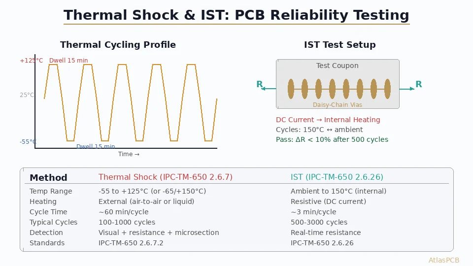
Interconnect Stress Testing (IST) — IPC-TM-650 2.6.26
IST is the industry-standard accelerated reliability test for via interconnects.
How IST works:
- A test coupon containing daisy-chained via structures is extracted from the production panel
- Direct current is applied to heat the coupon to a target temperature through resistive heating
- The coupon is heated from ambient to target in approximately 3 minutes
- The coupon is then cooled (forced air or natural convection) back to ambient in approximately 2 minutes
- Electrical resistance is measured continuously during the cycle
- The cycle repeats until failure or a predefined number of cycles is reached
Test conditions:
| Parameter | Standard (SnPb) | Lead-Free | High-Reliability |
|---|---|---|---|
| Target temperature | 150°C | 190°C | 190°C or 230°C |
| Cycle time | ~5 minutes | ~5 minutes | ~5 minutes |
| Failure criterion | >10% R increase | >10% R increase | >5% R increase |
| Minimum cycles (Class 2) | 300 | 300 | — |
| Minimum cycles (Class 3) | 500 | 500 | 1000 |
Advantages of IST:
- Fast: 500 cycles in ~42 hours (vs. weeks for thermal chamber cycling)
- Quantitative: Continuous resistance monitoring identifies degradation onset
- Representative: Direct heating mimics assembly reflow thermal stress
- Standardized: IPC-TM-650 method with clear pass/fail criteria
Thermal Shock — IPC-TM-650 2.6.7
Thermal shock testing uses rapid temperature transitions between hot and cold extremes.
Test conditions:
- Temperature range: -55°C to +125°C (standard) or -65°C to +150°C (military)
- Transfer time: <30 seconds between extremes
- Dwell time: 10–15 minutes at each extreme
- Cycle count: 100–1000 cycles depending on class
- Equipment: Two-chamber thermal shock cabinet or liquid bath
Why it matters: Thermal shock creates maximum mechanical stress due to the rapid temperature change. The extreme rate of thermal expansion/contraction is more damaging per cycle than gradual thermal cycling.
Thermal Cycling — IPC-TM-650 2.6.7
Similar to thermal shock but with slower temperature transitions:
- Temperature range: -40°C to +125°C (automotive) or -55°C to +125°C
- Ramp rate: 10–15°C/min
- Dwell time: 15–30 minutes at each extreme
- Cycle count: 500–2000+
- Cycle time: 45–90 minutes per cycle
Thermal cycling is more representative of field conditions but takes much longer than IST.
Microsection Analysis — IPC-TM-650 2.1.1
Destructive cross-section examination provides direct visual evidence of via quality:
What is examined:
- Copper barrel thickness (minimum, maximum, and distribution)
- Plating uniformity (throwing power ratio)
- Inner layer connection quality (no knee voids, no wedge voids)
- Via fill quality (dimple depth, void content)
- Microvia shape (taper angle, bottom diameter)
- Crack detection (barrel cracks, corner cracks, interface separation)
- Dielectric thickness between layers
Standard requirements (IPC-6012 Class 3):
- Minimum barrel plating: 20 µm (0.8 mil)
- Minimum inner layer connection: No void >25% of the pad width
- Dimple (for filled vias): ≤25 µm for standard, ≤15 µm for stacked microvias
- No cracks visible at 200× magnification
Solder Float Test — IPC-TM-650 2.4.13
A screening test for bulk via integrity:
- Apply flux to a test coupon
- Float the coupon on a solder pot at 288°C for 10 seconds
- Inspect for delamination, measling, or blistering
- Repeat for multiple cycles (3× minimum for Class 2, 6× for Class 3)
This test simulates the thermal stress of reflow assembly and rework. It is a pass/fail screening test, not a quantitative reliability assessment.
Reflow Simulation
Before formal testing, assess via survival through simulated reflow cycles:
- Profile: Match actual reflow profile (peak temperature, time above liquidus)
- Cycle count: 3× minimum (one initial + one for each side + one for rework)
- Assessment: Microsection after 3× and 6× reflow simulations
- Criteria: No cracks, no delamination, no resistance change >5%
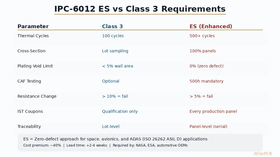
IPC-6012 Requirements
IPC-6012 Rev E defines three performance classes:
Class 1 — General Electronic Products
- Solder float: 1× at 288°C
- Thermal stress: Minimal requirements
- Microsection: Basic criteria
- Application: Consumer electronics, non-critical products
Class 2 — Dedicated Service Electronic Products
- Solder float: 3× at 288°C, 10 seconds each
- IST: 300 cycles at 150°C (SnPb) or 190°C (lead-free) without >10% R increase
- Microsection: Moderate criteria (20 µm barrel minimum)
- Application: Industrial, communications, general commercial
Class 3 — High-Reliability Electronic Products
- Solder float: 6× at 288°C, 10 seconds each
- IST: 500 cycles at 150°C (SnPb) or 190°C (lead-free) without >10% R increase
- Thermal shock: 100 cycles, -55°C to +125°C without failure
- Microsection: Stringent criteria (25 µm barrel minimum, extensive void limits)
- Application: Aerospace, military, medical, automotive safety-critical
Class 3/A — Space and Military Avionics
- Enhanced requirements beyond Class 3
- IST: 1000+ cycles
- Extended thermal cycling
- 100% microsection on representative samples
- Additional testing per MIL-PRF-31032 or similar
Microvia-Specific Reliability Concerns
Stacked Microvia Reliability
The industry learned a painful lesson about stacked microvia reliability in the 2015–2020 timeframe when several major OEMs experienced field failures in products using deep stacked microvias (4+ levels). Key findings:
- 1–2 stacked levels: Generally reliable with standard processes
- 3 stacked levels: Reliable with enhanced process control (fill quality, registration)
- 4 stacked levels: Requires qualification testing beyond standard IPC-6012 requirements
- 5+ stacked levels: High risk; requires extensive IST qualification at elevated conditions
IPC-6012 Rev E Microvia Additions
In response to field failures, IPC-6012 Rev E added specific microvia reliability requirements:
- Microvia IST: Separate test coupons for microvia structures (not just through-hole vias)
- Stacked via qualification: Additional testing for stacked structures beyond 2 levels
- Fill quality criteria: Tighter dimple and void specifications for stacked vias
Industry Best Practices for Microvia Qualification
- Design IST coupons that match your actual via structures: Include single microvias, stacked 2-level, stacked 3-level, etc.
- Test at 190°C or higher: Lead-free assembly temperatures demand testing at elevated conditions
- Extend cycle counts: Run at least 500 cycles, preferably 1000+ for critical applications
- Include preconditioning: Subject coupons to 6× reflow simulation before IST to represent real-world assembly stress
- Cross-section after IST: Microsection IST coupons at various cycle intervals (100, 300, 500, 1000) to understand crack initiation and propagation
Test Coupon Design
Types of Test Coupons
- Through-hole daisy chain: Series-connected through-hole vias for IST/thermal cycling. Typical: 50–100 vias in series.
- Microvia daisy chain: Series-connected microvias (single, stacked, staggered) for IST.
- Impedance coupon: Transmission line structures for TDR impedance measurement.
- Microsection coupon: Dedicated areas for cross-section analysis at various points on the panel.
- IST coupon: Combined structure per IPC-TM-650 2.6.26 with both through-hole and microvia chains.
Coupon Placement
- Place coupons in the panel border (tooling strip), not within the board array
- Include coupons at multiple locations on the panel (corners, center) to capture process variation
- Each unique via structure in the design should have a corresponding test coupon
Coupon Requirements per IPC-2221
- Minimum 2 coupons per panel for impedance
- Minimum 1 coupon per panel for microsection
- IST coupons: per production lot or per panel (depending on reliability class)
Reliability Improvement Strategies
Material Selection
- Low Z-axis CTE laminate: Choose materials with CTE <3% (50–260°C). Examples: Isola 370HR, Panasonic Megtron 6.
- High Tg materials: Tg ≥170°C ensures the board stays below Tg during normal operation, where CTE is lowest.
- Low Td materials are risky: Ensure Td ≥340°C for lead-free assembly compatibility.
Process Optimization
- Plating thickness: Target minimum 25 µm in barrel for Class 3 (vs. 20 µm specification)
- Plating uniformity: Pulse/PPR plating for high aspect ratio vias
- Fill quality: For stacked microvias, target dimple <10 µm with <5% void area
- Desmear: Ensure complete desmear with plasma for microvia structures
- Laser drilling parameters: Optimize for clean, round via shapes with minimal taper
Design Rules
- Limit stacked depth: 3 levels maximum unless fully qualified with extended IST
- Via aspect ratio: ≤0.75:1 for microvias, ≤12:1 for through-holes (standard processes)
- Pad size: Provide adequate annular ring (≥50 µm for microvias, ≥75 µm for through-holes)
- Avoid mixing via types: Don’t land a through-hole on a microvia pad; the mechanical stress profile is incompatible
Interpreting Test Results
IST Resistance Curves
A healthy IST curve shows stable resistance through the test cycles with <5% variation. Warning signs:
- Gradual resistance increase: Indicates progressive crack growth. The via will eventually fail.
- Intermittent spikes: Suggest a crack that opens and closes during thermal cycling. Very dangerous — the via may test “good” at room temperature but fail at elevated temperature.
- Sudden step increase: Indicates a major crack or separation event.
When to Investigate Further
- Any resistance increase >5% before the target cycle count
- More than 10% variation between coupon positions on the same panel
- Microsection showing any visible cracking at 200×, even if resistance is stable
Conclusion
Via reliability testing is not optional for products that need to work reliably through their intended service life. IST, thermal cycling, and microsection analysis provide complementary views into via health—IST for accelerated screening, thermal cycling for field-representative qualification, and microsection for root cause analysis.
At Atlas PCB , our quality system includes comprehensive via reliability testing per IPC-6012 and IPC-TM-650. We provide IST coupons on every HDI panel and maintain historical reliability data for our standard via structures. Request a quote and our engineering team will recommend appropriate reliability testing for your specific design.
For related reading, see our guides on [HDI PCB stackup design]/blog/hdi-pcb-stackup-design-advanced/), [HDI PCB technology]/blog/hdi-pcb-technology/), and [multilayer PCB manufacturing]/blog/multilayer-pcb-manufacturing-process-explained/).
Further Reading
- [HDI PCB Design Guide: Stackup Rules, Via Structures & DFM Checklist]/blog/hdi-pcb-design-guide/)
- [High-Multilayer FR4 vs Standard FR4: When to Upgrade Material Grade]/blog/high-multilayer-fr4-vs-standard-fr4/)
- [Multilayer PCB Stackup Design Guide: 8 to 30+ Layers Step by Step]/blog/multilayer-pcb-stackup-design-guide/)
About AtlasPCB — We specialize in complex PCB manufacturing for HDI, RF, and high-reliability applications. Explore our HDI PCB manufacturing capabilities, aluminum and metal-core PCB services, or get an full PCB manufacturing capabilities . Every order includes free engineering review. Get your quote.
Reviewed by AtlasPCB Engineering Team — IPC-certified manufacturing specialists with 15+ years of production experience in HDI, RF, and high-reliability PCB fabrication. Content based on factory floor data and real customer design reviews.
- via reliability
- IST
- thermal cycling
- IPC-6012
- microvia
- HDI