· AtlasPCB Engineering · Engineering · 11 min read
PCB Aspect Ratio: Via Depth-to-Diameter Rules and Manufacturing Limits
A comprehensive guide to PCB via aspect ratios covering through-hole, blind, and buried vias. Learn IPC recommendations, manufacturing capability limits, and how aspect ratio impacts reliability.
PCB Aspect Ratio: Via Depth-to-Diameter Rules and Manufacturing Limits
Via aspect ratio is one of the most critical — and most frequently misunderstood — parameters in PCB design. Get it wrong, and you end up with boards that fail plating inspection, crack during thermal cycling, or simply cannot be manufactured at a reasonable cost. Get it right, and you unlock reliable high-density interconnects that perform across thousands of thermal cycles.
This guide covers everything a PCB designer or engineer needs to know about via aspect ratios: the fundamental definitions, IPC guidelines, real-world manufacturing limits for through-hole, blind, and buried vias, and practical design strategies to keep your boards manufacturable and reliable.
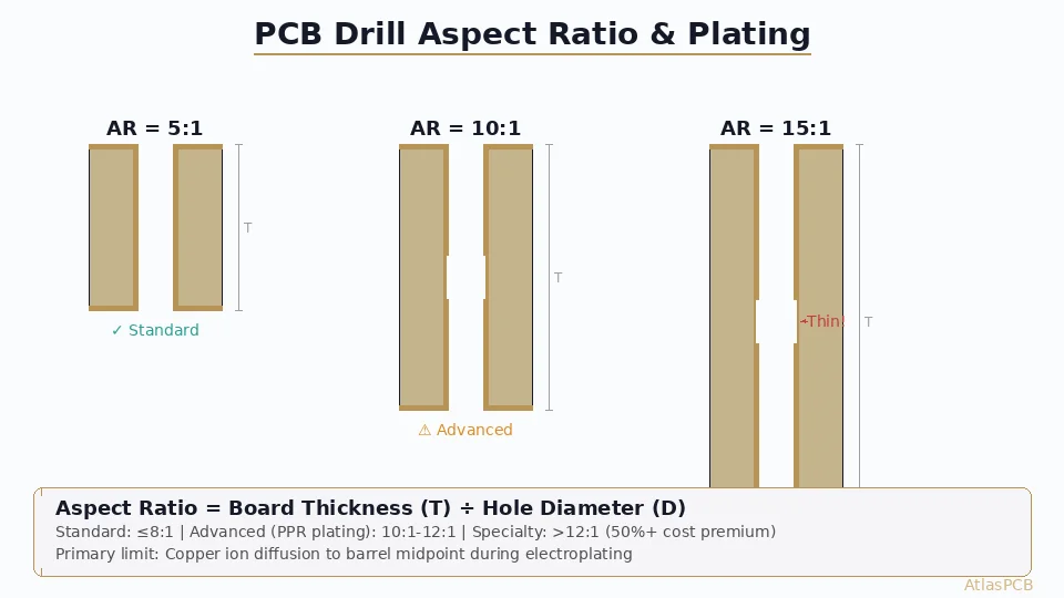
What Is Via Aspect Ratio?
Via aspect ratio is defined as the ratio of the via’s depth to its drilled (or finished) hole diameter:
Aspect Ratio = Via Depth ÷ Drilled Hole Diameter
For a through-hole via, the depth equals the total board thickness. For a blind via, the depth is the distance from the surface to the target inner layer. For a buried via, the depth is the thickness of the sub-lamination containing the via.
Consider a standard 1.6 mm (63 mil) thick PCB with a 0.2 mm (8 mil) drilled through-hole via. The aspect ratio is:
1.6 mm ÷ 0.2 mm = 8:1
This single number tells the fabricator — and the designer — a great deal about how difficult the via will be to plate, how reliable it will be in the field, and how much it will cost to produce.
Why Aspect Ratio Matters
Electroplating Uniformity
The primary challenge with high-aspect-ratio vias is electroplating. During the copper electroplating process, fresh electrolyte must reach the center of the via barrel to deposit copper uniformly. In a deep, narrow hole, the electrolyte exchange rate at the center drops dramatically compared to the entrance. This leads to a phenomenon called the throwing power limitation, where copper deposits thickly at the via entrance and thinly at the center.
IPC-6012 Rev F specifies minimum copper plating thickness requirements:
- Class 2: Minimum 20 µm (0.8 mil) average, 18 µm (0.7 mil) at any point in the barrel
- Class 3: Minimum 25 µm (1.0 mil) average, 20 µm (0.8 mil) at any point
Meeting these minimums becomes progressively harder as the aspect ratio increases. At 8:1, standard DC plating struggles to maintain uniformity. At 10:1 and above, pulse plating or reverse-pulse plating (PPR) becomes necessary to achieve acceptable throwing power.
Thermal Reliability
During thermal cycling — whether from reflow soldering or operational temperature swings — the via barrel expands along its length (Z-axis). The copper plating must absorb this strain without cracking. A thin spot in the barrel, which is precisely what a high aspect ratio tends to create, becomes the crack initiation site.
IPC-TM-650 Method 2.6.26 (Interconnect Stress Test, or IST) subjects vias to repeated thermal cycles from approximately 25°C to 150°C or 190°C. The failure criterion is typically a 10% increase in resistance. High-aspect-ratio vias with marginal plating consistently fail IST testing earlier than lower-aspect-ratio equivalents.
Manufacturability and Cost
Beyond reliability, aspect ratio directly impacts yield. As aspect ratio increases:
- Drilling becomes more difficult — drill bits deflect more in deep holes, leading to positional inaccuracy and rough hole walls
- Desmear (the process of removing resin smear from inner layer connections) becomes less effective in deep, narrow holes
- Plating requires more sophisticated chemistry and process controls
- Inspection must be more thorough, often requiring cross-sectioning
All of these factors increase cost. A board with 6:1 aspect ratio through-hole vias will be significantly cheaper to fabricate than the same design with 10:1 vias.
Through-Hole Via Aspect Ratios
Through-hole vias traverse the entire board thickness. Their aspect ratio is governed by board thickness and minimum drill size.
Standard Manufacturing Capabilities
| Board Thickness | Min Drill (8:1) | Min Drill (10:1) | Min Drill (12:1) |
|---|---|---|---|
| 1.0 mm (39 mil) | 0.125 mm (5 mil) | 0.10 mm (4 mil) | 0.083 mm (3.3 mil) |
| 1.6 mm (63 mil) | 0.20 mm (8 mil) | 0.16 mm (6.3 mil) | 0.133 mm (5.3 mil) |
| 2.0 mm (79 mil) | 0.25 mm (10 mil) | 0.20 mm (8 mil) | 0.167 mm (6.6 mil) |
| 2.4 mm (94 mil) | 0.30 mm (12 mil) | 0.24 mm (9.4 mil) | 0.20 mm (8 mil) |
| 3.2 mm (126 mil) | 0.40 mm (16 mil) | 0.32 mm (12.6 mil) | 0.267 mm (10.5 mil) |
Industry Tiers
- Standard fabricators (most offshore): 8:1 maximum, mechanical drilling only, 0.2 mm minimum drill
- Advanced fabricators: 10:1, pulse plating available, 0.15 mm minimum drill
- Specialty/high-reliability fabricators: 12:1 to 15:1, PPR plating, advanced desmear, 0.1 mm minimum mechanical drill
- Military/aerospace certified: Typically limited to 8:1 per internal specs, even if manufacturer can do more
IPC Guidelines
IPC-6012 does not explicitly state a maximum aspect ratio. Instead, it specifies plating thickness and integrity requirements that become increasingly difficult to meet at higher ratios. The practical effect is:
- Class 1 (General Electronics): 10:1 is generally achievable
- Class 2 (Dedicated Service Electronics): 8:1 is the comfortable limit; 10:1 with process validation
- Class 3 (High-Reliability): 8:1 is the practical limit; anything above requires extensive qualification
IPC-2221B (Generic Standard on Printed Board Design) Section 9.1.1 recommends that designers consult with their fabricator when aspect ratios exceed 8:1.
Blind Via Aspect Ratios
Blind vias connect an outer layer to one or more inner layers without passing through the entire board. They come in two primary types: mechanically drilled and laser drilled (microvias).
Laser-Drilled Microvias
Laser-drilled microvias, as used in [HDI PCB technology]/blog/hdi-pcb-technology/), are the workhorses of modern high-density design. They are typically drilled with CO2 or UV lasers and span a single dielectric layer (about 50–100 µm).
Standard microvia aspect ratio limits:
- 0.8:1 to 1:1 — Standard capability for most HDI fabricators
- 1.0:1 — The most common design rule; e.g., 75 µm depth with 75 µm diameter
- 1.5:1 — Achievable with UV laser and advanced plating, but not standard
- >1.5:1 — Requires specialized processes; not recommended for production
Per IPC-2226 (HDI design standard), microvias are defined as having a hole diameter of ≤150 µm (6 mil). The aspect ratio for single-layer microvias should not exceed 1:1 for reliable copper fill plating.
Mechanically Drilled Blind Vias
When blind vias span two or more dielectric layers (e.g., L1 to L3 in an 8-layer board), they are typically mechanically drilled with controlled-depth drilling. The aspect ratio considerations are:
- Depth control: Mechanical drills must stop at a precise depth, typically ±50 µm (2 mil). Deeper holes are harder to control.
- Aspect ratio limit: Generally 1:1 to 1.5:1, with 0.8:1 recommended for production reliability
- Minimum diameter: 0.15 mm (6 mil) for most fabricators; 0.1 mm (4 mil) for advanced shops
The challenge with mechanically drilled blind vias is not just plating — it’s also drill depth accuracy. A drill that goes too deep damages the target pad; too shallow and there’s no connection. This is why many designers prefer [sequential lamination with laser microvias]/blog/pcb-via-size-selection-guide/) over deep controlled-depth drilling.

Buried Via Aspect Ratios
Buried vias connect two or more inner layers and are completely enclosed within the board after lamination. They are fabricated during sub-lamination, before the final press.
Design Considerations
Since buried vias are drilled through a thin sub-lamination (often 0.2 mm to 0.8 mm), their aspect ratios are typically more manageable than full-thickness through-hole vias. However, the same plating principles apply:
- Typical aspect ratios: 4:1 to 8:1
- Sub-lamination thickness: The key variable; thinner subs allow smaller drills
- Registration: Buried vias must align with inner layer artwork during lamination — misregistration is a common defect mode
For a 0.4 mm thick sub-lamination with a 0.1 mm drill, the aspect ratio is 4:1 — well within standard capabilities.
Sequential Lamination and Aspect Ratio Stacking
In complex HDI boards with multiple sequential lamination cycles, the total number of laminations impacts via reliability. Each lamination cycle subjects previously formed vias to additional thermal stress. A buried via with a borderline aspect ratio may survive its initial plating inspection but fail after exposure to multiple lamination press cycles at 180–200°C.
Best practice: Keep buried via aspect ratios at 6:1 or below when the sub-lamination will undergo two or more additional press cycles.
Practical Design Strategies
1. Choose Board Thickness Wisely
The simplest way to improve aspect ratio is to reduce board thickness. If your design doesn’t require a thick board, consider:
- 1.0 mm instead of 1.6 mm for 4–6 layer boards — cuts aspect ratio by 37%
- 0.8 mm for compact assemblies — achieves excellent aspect ratios even with small vias
- Work with your fabricator to determine the minimum viable thickness for your layer count
2. Right-Size Your Vias
Not every via needs to be the smallest possible. Use a tiered via strategy:
- Power/ground vias: 0.3–0.4 mm drill — easy to plate, low resistance
- Signal vias: 0.2–0.25 mm drill — good balance of density and manufacturability
- Fine-pitch escape vias: 0.15–0.2 mm drill — only where BGA pitch demands it
- Microvias: 0.075–0.1 mm laser drill — for HDI layers only
3. Use Microvias to Reduce Through-Via Demands
Instead of routing a signal through the entire board with a single high-aspect-ratio through-hole via, consider a via-in-pad with microvia structure. A surface microvia connects to a buried via or through-hole via with a larger diameter. This approach, detailed in our [via size selection guide]/blog/pcb-via-size-selection-guide/), keeps each individual via well within its optimal aspect ratio range.
4. Communicate Early With Your Fabricator
Aspect ratio capability varies significantly between fabricators. Before finalizing your design:
- Share your proposed stackup and via table
- Ask for the fabricator’s proven (not theoretical) aspect ratio limit
- Request a cross-section report from a similar recent build
- Discuss whether pulse plating or PPR is available and at what cost premium
5. Design for Your Reliability Class
Match your aspect ratio targets to your end-use environment:
| Application | Recommended Max AR | Justification |
|---|---|---|
| Consumer electronics | 10:1 | Short lifecycle, benign environment |
| Industrial | 8:1 | Moderate thermal cycling, 10+ year life |
| Automotive | 8:1 | Extreme thermal cycling, vibration |
| Aerospace/Defense | 6:1 to 8:1 | Maximum reliability, long field life |
| Medical implant | 6:1 | Zero-defect requirement |
Aspect Ratio and Plating Technology
The march toward higher aspect ratios has been enabled by advances in plating chemistry:
DC Plating
The traditional method. Throwing power is limited, making it suitable for aspect ratios up to approximately 6:1 to 8:1 depending on the chemistry.
Pulse Plating
By alternating between plating current and rest periods, pulse plating allows fresh electrolyte to diffuse into the via center. Effective up to approximately 10:1.
Reverse Pulse Plating (PPR)
PPR alternates between forward plating and brief reverse (dissolving) pulses. The reverse pulse preferentially removes copper from the via entrance where it’s thickest, improving uniformity. This technology enables aspect ratios of 12:1 and above.
Via Fill Plating
For microvias and small through-hole vias, via fill plating (also called copper-filled vias) uses specialized chemistry to fill the via completely with copper. This is essential for via-in-pad designs and [stacked microvia structures]/blog/hdi-pcb-technology/). Via fill plating works best at lower aspect ratios (≤1:1 for microvias, ≤6:1 for through-holes being filled).
Testing and Verification
Cross-Sectioning (Microsection Analysis)
The gold standard for verifying plating quality. A via is sliced in half, polished, and examined under a microscope. Measurements include:
- Minimum barrel plating thickness
- Plating uniformity (ratio of center thickness to entrance thickness)
- Knee/corner plating thickness
- Presence of voids, cracks, or inclusions
Per IPC-6012, three cross-sections per coupon are typically required, with measurements at multiple points.
IST (Interconnect Stress Test)
Per IPC-TM-650 2.6.26, IST applies thermal stress by resistive heating and measures resistance change. It directly tests via barrel integrity without the statistical ambiguity of thermal cycling ovens.
4-Wire Resistance Measurement
Simple daisy-chain resistance measurements on test coupons can detect via plating anomalies before expensive cross-sectioning.
Common Pitfalls
Ignoring finished vs. drilled diameter: Aspect ratio should be calculated from the drilled diameter, not the finished (plated) diameter. After plating, the hole shrinks by approximately 50 µm (2 mil), but the depth doesn’t change.
Forgetting panel plating buildup: In pattern-plating processes, the via barrel gets plated during both panel plating and pattern plating. In panel-plating-only processes, only one plating step fills the barrel. Understand your fab’s process flow.
Using different aspect ratios for the same board without realizing it: A 2.4 mm thick board might have 0.3 mm vias (8:1) and 0.2 mm vias (12:1) on the same design. The 12:1 vias will drive cost and risk.
Not accounting for back-drill depth: Back-drilled vias have a reduced effective depth, which actually improves the plated aspect ratio. But the back-drill itself introduces new mechanical challenges.
Summary
Via aspect ratio is a deceptively simple number that governs a complex interplay of drilling, plating, and reliability physics. For most designs:
- Stay at or below 8:1 for through-hole vias whenever possible
- Keep microvias at 1:1 or below for reliable fill plating
- Design buried via aspect ratios at 6:1 or below for multi-press stackups
- Consult your fabricator before pushing beyond standard limits
- Match aspect ratio to reliability class — don’t over-design consumer products or under-design aerospace hardware
Understanding and controlling aspect ratio is fundamental to creating PCBs that are manufacturable, reliable, and cost-effective. When in doubt, get a quote and let our engineering team review your design for manufacturability.
Ready to start your project? Upload your Gerbers for a free engineering review, or talk to an engineer about your design requirements.
Further Reading
- [Rogers PCB Fabrication: Material Sourcing, Lead Times & Quality Control]/blog/rogers-pcb-fabrication/)
- [PCB Rigid-Flex Bend Zone Reliability: Design Rules, Material Selection & Lifecycle Testing]/blog/pcb-rigid-flex-bend-zone-reliability/)
- [Plating Void Prevention in PCB Vias]/blog/pcb-plating-void-prevention/)
- [ENEPIG vs ENIG Surface Finish: Complete Comparison for Wire Bonding, Solderability, and Long-Term Reliability]/blog/enepig-vs-enig-surface-finish-wire-bonding/)
- [PCB Surface Finish Comparison: OSP vs HASL vs Immersion Silver vs ENIG for Assembly Reliability]/blog/pcb-surface-finish-osp-hasl-enig-immersion-silver-comparison/)
- Our Manufacturing Capabilities
About AtlasPCB — We specialize in complex PCB manufacturing for HDI, RF, and high-reliability applications. Explore our full PCB manufacturing capabilities, or get an instant online quote . Every order includes free engineering review. Get your quote.
Reviewed by AtlasPCB Engineering Team — IPC-certified manufacturing specialists with 15+ years of production experience in HDI, RF, and high-reliability PCB fabrication. Content based on factory floor data and real customer design reviews.
- aspect-ratio
- via-design
- pcb-manufacturing
- reliability