· AtlasPCB Engineering · Engineering · 3 min read
How to Specify Impedance on Your PCB: Stackup Notes & Fab Drawing Tips
Practical guide to specifying controlled impedance on PCB fabrication drawings. Covers impedance table format, stackup documentation, tolerance specifications, TDR coupon design, and communication best practices with your PCB manufacturer.
How to Specify Impedance on Your PCB: Stackup Notes & Fab Drawing Tips
Getting controlled impedance right starts long before manufacturing—it starts with how you communicate your requirements to the fabricator. A well-documented impedance specification eliminates guesswork, reduces the need for costly re-spins, and ensures your production boards match your simulation results.
This guide covers the practical details of specifying impedance on your PCB: what to include in your fabrication drawing, how to format impedance tables, stackup documentation best practices, and the communication workflow with your manufacturer.
What to Include in Your Impedance Specification
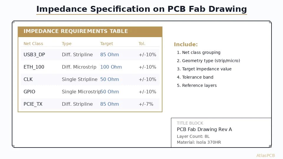
The Impedance Control Table
Every impedance-controlled design should include a table in the fabrication notes with these columns:
| Column | Example | Purpose |
|---|---|---|
| Net Class | USB3_DP | Identifies the signal group |
| Impedance Type | Differential | SE, differential, or coplanar |
| Target Impedance | 90Ω ±5% | Value and tolerance |
| Signal Layer | L3 | Which copper layer |
| Reference Layer | L2 (GND) | Adjacent reference plane |
| Trace Width | 4.0 mil (target) | Designer’s starting value |
| Trace Spacing | 5.0 mil | For differential pairs |
| Copper Weight | 0.5 oz | Signal layer copper |
Example impedance table:
| Net Class | Type | Target | Tolerance | Signal Layer | Reference | Width | Space |
|---|---|---|---|---|---|---|---|
| CLK_100 | Single-ended | 50Ω | ±5% | L1 | L2 (GND) | 4.5 mil | — |
| USB3_DP/DN | Differential | 90Ω | ±5% | L3 | L2 (GND) | 4.0 mil | 5.0 mil |
| PCIE_TX | Differential | 85Ω | ±5% | L5 | L4 (GND) | 4.0 mil | 6.0 mil |
| DDR4_DQ | Single-ended | 40Ω | ±10% | L1 | L2 (GND) | 5.0 mil | — |
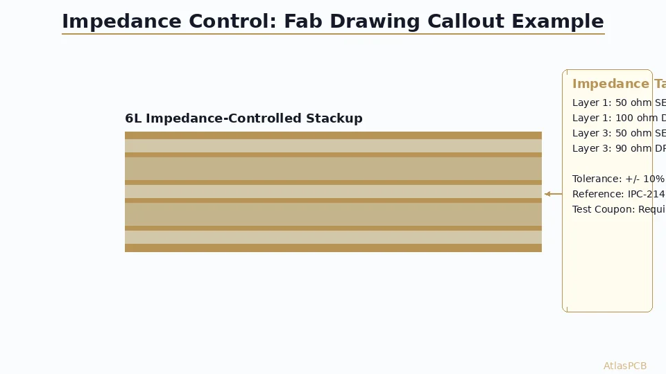
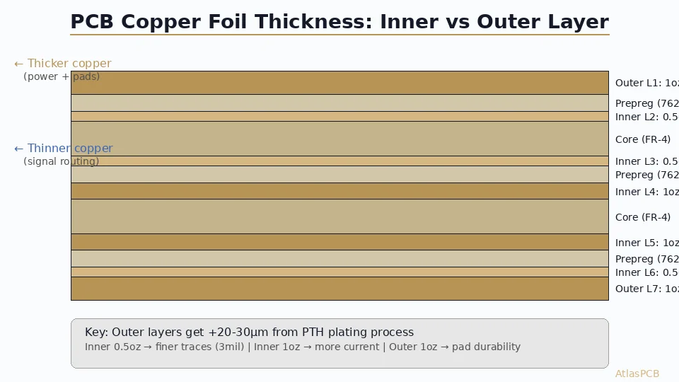
Stackup Documentation
Include a complete stackup cross-section showing:
- Layer numbers and functions (signal, ground, power)
- Copper weight for each layer
- Dielectric material and thickness between each layer pair
- Total board thickness with tolerance
- Material specification (e.g., “Isola 370HR or equivalent, Dk ≤ 4.2 @ 1 GHz”)
Critical note: Specify “or equivalent” with a Dk range rather than a single material. This gives the fabricator flexibility to use available stock while maintaining your impedance targets. The fabricator will adjust trace widths based on their actual material’s Dk.
Tolerance Specification
| Tolerance | Application | Cost Impact | Verification |
|---|---|---|---|
| ±10% | General digital, IPC default | Baseline | Process control only |
| ±7% | Mid-range, DDR3/4 | +5% | Coupon recommended |
| ±5% | High-speed (PCIe, USB3, 10G+) | +10-15% | Coupon mandatory |
| ±3% | RF/microwave | +25-40% | Every board TDR tested |
For detailed impedance control methodology, see our [PCB impedance control guide]/blog/pcb-impedance-control/).

TDR Test Coupon Design
Coupon Types
| Coupon | Measures | Minimum Length |
|---|---|---|
| Microstrip SE | Single-ended outer layer impedance | 6 inches |
| Microstrip differential | Differential outer layer impedance | 6 inches |
| Stripline SE | Single-ended inner layer impedance | 6 inches |
| Stripline differential | Differential inner layer impedance | 6 inches |
Coupon Placement
- Place coupons on the panel border (breakaway area), not on the board itself
- Include all impedance variations present in your design
- Ensure coupons use the same dielectric spacing as the corresponding board layers
- Add launch pads compatible with the fabricator’s TDR probe (typically SMA or microprobe)
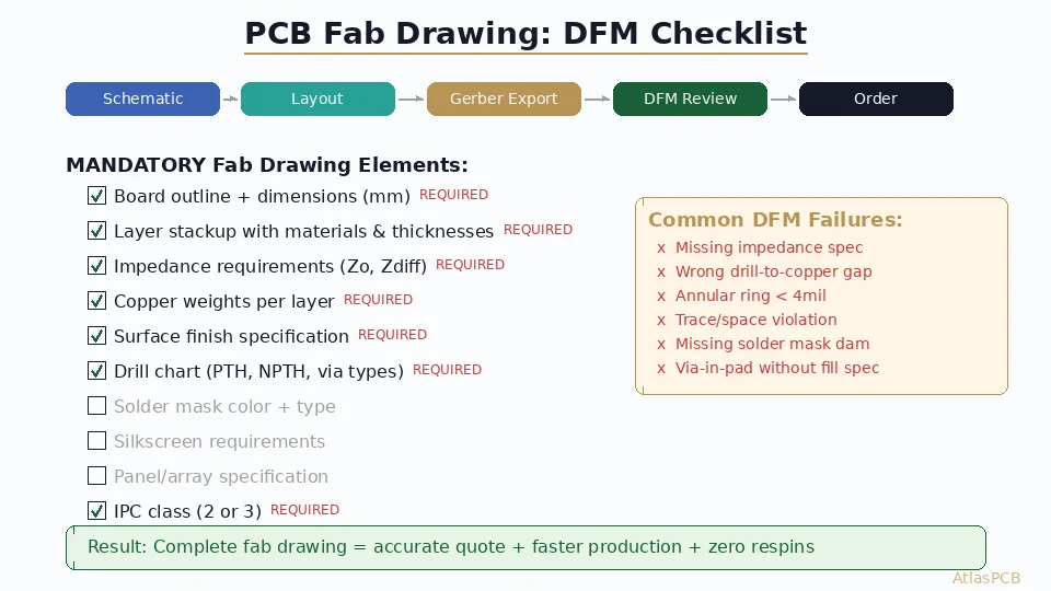
Communication Best Practices
What to Send Your Fabricator
- Gerber files (RS-274X or Gerber X2 with embedded attributes)
- Drill files (Excellon format with plated/non-plated separation)
- Fabrication drawing (PDF) with impedance table, stackup, and manufacturing notes
- Stackup file (if available from your EDA tool—Altium .stackup, Allegro .brd)
- README or specification document highlighting critical requirements
Common Impedance Specification Mistakes
- Specifying trace width without impedance target: Trace width is a means, impedance is the requirement. Let the fabricator optimize width for their materials.
- Forgetting to specify the reference layer: Impedance depends on dielectric thickness to the reference plane—ambiguity here causes errors.
- Using simulation Dk values as specifications: Your field solver uses ideal Dk; the fabricator’s actual material varies. Specify impedance, not Dk.
- Not accounting for copper roughness: At frequencies above 3 GHz, copper roughness significantly affects impedance. Specify low-profile copper if needed.
For stackup documentation best practices, see our [PCB stackup design guide]/blog/pcb-stackup-design-guide/) and [controlled impedance PCB guide]/blog/controlled-impedance-pcb/).
Ready to get your impedance-controlled board manufactured? Upload your Gerbers with your impedance specifications for a free engineering review.
Further Reading
- [PCB Impedance Control: How to Achieve ±5% Tolerance]/blog/pcb-impedance-control/)
- [Controlled Impedance PCB: Design, Stackup & Testing]/blog/controlled-impedance-pcb/)
- [PCB Stackup Design Guide]/blog/pcb-stackup-design-guide/)
About AtlasPCB — We specialize in complex PCB manufacturing for HDI, RF, and high-reliability applications. Explore our impedance-controlled PCB manufacturing . Every order includes free engineering review. Get your quote.
Reviewed by AtlasPCB Engineering Team — IPC-certified manufacturing specialists with 15+ years of production experience in HDI, RF, and high-reliability PCB fabrication. Content based on factory floor data and real customer design reviews.
- impedance-control
- pcb-design
- fab-drawing
- manufacturing