· AtlasPCB Engineering · Engineering · 9 min read
How to Specify Backdrilling in Your PCB Fab Notes: Depth, Tolerances, and Drawing Callouts
Complete guide to specifying backdrilling (controlled-depth drilling) in your PCB fabrication notes. Covers stub length calculations, depth tolerance callouts, drawing annotations, and common mistakes that cause signal integrity failures or manufacturing rejections.
The 60-Second Backdrill Specification Checklist
Before sending your design to fabrication, verify your fab notes include all of these:
- Backdrill table with: drill ID, from-side, target layer, finished BD hole size, max stub length
- Depth tolerance callout (default: +/-3mil unless negotiated)
- Backdrill diameter specified (typically via drill + 8mil)
- Clear identification of which vias require backdrilling (by net class, drill chart, or explicit callout)
- Cross-section reference detail for complex multi-layer cases
- Acceptance criteria: max stub length OR target depth from reference datum
If your fab drawing is missing any of these, expect a fabrication hold and 2-5 days of back-and-forth clarification.
Why Your Fab Drawing Probably Gets Backdrilling Wrong
Most signal integrity engineers understand why backdrilling matters — removing unused via stubs eliminates the quarter-wave resonance that creates notches in your channel’s insertion loss response. A 100mil stub resonates at approximately 15 GHz, which lands squarely in the Nyquist frequency of 28 Gbps NRZ signals. The physics is well understood.
What is poorly understood is how to communicate backdrill requirements to a fabricator in a way that results in correct, first-pass manufacturing. The disconnect happens because PCB designers think in terms of signal layers and impedance targets, while fabricators work with physical drill depths measured from a mechanical reference datum (usually the board surface). Bridging that gap requires precise drawing callouts that translate your electrical requirement into a mechanical manufacturing specification.
The most common failure mode is not incorrect backdrilling — it is no backdrilling specification at all. Engineers assume the fabricator will “figure it out” from the layer stackup and net class assignments. In reality, without explicit fab note instructions, most fabricators will ship boards with full-length via stubs, and you will discover the problem during TDR measurements or compliance testing weeks later.
BACKDRILLING EXPERTISE
Backdrill Depth Accuracy: +/-3mil Guaranteed
AtlasPCB uses laser-monitored CNC backdrilling with coupon verification on every panel. We review your backdrill spec before production to catch common drawing errors.
Upload Gerber ›The Backdrill Table: Exact Format Your Fabricator Needs
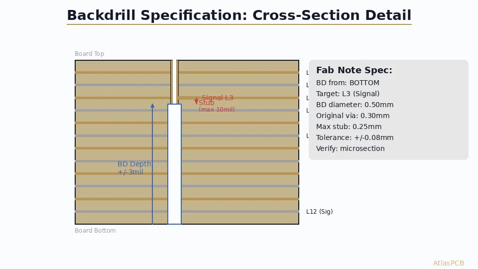
Your fab drawing should include a dedicated backdrill table. Here is the format that eliminates ambiguity:
| BD ID | Drill From | Target Signal Layer | BD Hole Dia | Original Via Dia | Max Stub | Tolerance |
|---|---|---|---|---|---|---|
| BD1 | Top | L3 (Signal) | 0.50mm | 0.30mm | 0.25mm | +/-0.08mm |
| BD2 | Bottom | L6 (Signal) | 0.50mm | 0.30mm | 0.25mm | +/-0.08mm |
| BD3 | Top | L5 (Signal) | 0.45mm | 0.25mm | 0.13mm | +/-0.08mm |
The critical columns are:
Drill From: Specifies which board surface the backdrill enters from. This seems obvious but becomes essential for asymmetric stackups and dual-side backdrilling where the same via might be backdrilled from both directions.
Target Signal Layer: The layer where your signal trace connects to the via. The fabricator uses this plus your stackup to calculate the mechanical drill depth. Always reference layer numbers (L3, L6) rather than functional names (“inner signal 2”) to avoid misinterpretation.
Max Stub Length: Your electrical requirement expressed as the maximum remaining copper barrel below the signal layer. This is what the fabricator’s quality team measures during cross-section inspection. Specifying this rather than a drill depth allows the fabricator to account for stackup thickness variation between panels.
Tolerance: The acceptable variation in backdrill depth. Standard capability is +/-3mil (0.08mm). If you need tighter, discuss with your fabricator before committing — not all facilities have the equipment for +/-2mil accuracy.
Calculating Backdrill Depth from Your Stackup
The fabricator converts your stub length requirement into a physical drill depth using your stackup dimensions. Understanding this calculation helps you verify their engineering review and catch errors before production.
The formula is straightforward. For a top-side backdrill targeting a signal on Layer N:
Backdrill Depth = Total thickness from top surface to Layer N - Max Stub Length - Tolerance
For example, in a 12-layer 2.0mm board where the signal connects on Layer 4 (0.65mm from top surface):
- Target depth = 0.65mm - 0.25mm (stub) - 0.08mm (tolerance margin) = 0.32mm programmed depth
- Worst case stub = 0.25mm + 0.08mm = 0.33mm (still acceptable for most 16 Gbps applications)
- Best case: drill hits exactly, stub = 0.25mm - 0.08mm = 0.17mm
The key insight is that your specified “max stub” must already include the tolerance margin. If your channel simulation shows failure at 10mil stub, do not specify “10mil max stub” — specify “7mil max stub” to ensure worst-case (7mil + 3mil tolerance) still meets your electrical requirement.
This is where many designers make their first mistake: specifying the absolute maximum acceptable stub without accounting for drilling tolerance, which results in a small but real percentage of boards exceeding the electrical limit.
HIGH-SPEED DESIGN SUPPORT
We Verify Your Backdrill Specs Before Production
Our engineering team cross-checks your backdrill callouts against the actual stackup to ensure drill depths and stub lengths are physically achievable. No manufacturing surprises.
HDI Capabilities ›Fab Drawing Annotation: What Goes Where
Beyond the backdrill table, your fab drawing needs specific annotations placed correctly. Here is what experienced fabricators expect to see:
In the drill chart: Add backdrill tools with a “BD” prefix. Example:
- BD1: 0.50mm backdrill, qty 124, from TOP, note “See backdrill table”
- BD2: 0.50mm backdrill, qty 88, from BOTTOM, note “See backdrill table”
In the layer stackup detail: Show a cross-section callout with the backdrill geometry drawn explicitly. Include dimension arrows showing the target stub length and the backdrill entry surface. This visual catches interpretation errors that a text-only specification might miss.
In the general fab notes: Include a blanket statement such as: “All backdrilling per table on sheet 2. Max stub length measured from target signal layer to bottom of backdrill hole. Verify by cross-section on coupon per IPC-TM-650 2.1.1. Stub measurement tolerance per IPC-6012E section 3.6.2.11.”
In the acceptance criteria section: State explicitly: “Backdrill stub length shall not exceed values specified in backdrill table. Verification: microsection 3 locations per panel (one each: top BD, bottom BD, dual BD if applicable).”
The reference to IPC-6012E section 3.6.2.11 is important because it establishes a shared understanding of measurement methodology. Without it, debates about how to measure the stub (from which reference point, at what location in the hole) can delay acceptance.
Common Specification Mistakes (and How to Fix Them)
Mistake 1: Specifying backdrill depth instead of stub length. Why it fails: Board thickness varies +/-10% between panels. A fixed drill depth produces variable stub lengths. Always specify max stub length and let the fabricator calculate depth per their actual measured stackup.
Mistake 2: Backdrill diameter too small. Symptoms: Residual copper barrel remains after backdrilling, creating a partial stub. Fix: Ensure BD diameter is at least 8mil larger than the original PTH drill to account for drill registration accuracy.
Mistake 3: No specification for which vias to backdrill. What happens: Fabricator either skips backdrilling entirely or backdrills everything (including vias that connect to internal layers within the backdrill zone — breaking connectivity). Fix: Identify backdrilled vias by drill chart entry, net class assignment, or explicit callout on the drill drawing.
Mistake 4: Backdrilling into an active signal layer. A dual-side backdrill where the top BD and bottom BD have overlapping depth targets can remove copper on intermediate signal layers. Fix: Verify that the shortest distance between opposing backdrill bottoms exceeds 10mil plus twice the tolerance. For a 2.0mm board with top BD to L4 (0.65mm deep) and bottom BD to L9 (0.65mm deep), the gap = 2.0mm - 0.65mm - 0.65mm = 0.70mm — plenty of margin.
Mistake 5: Not accounting for copper layer thickness in depth calculation. The signal layer is not infinitely thin — it has 1.2-1.7mil (35-43um) of copper after plating. Your stub measurement should reference the far side (bottom) of the copper layer, not its center. This 1-2mil difference matters for aggressive 5mil stub specs.
When Backdrilling Is Not the Answer
Backdrilling is a subtractive process with inherent limitations. For designs where via stub control tighter than +/-3mil is required, or where the stub needs to be eliminated entirely (0mil residual), consider these alternatives:
Blind/buried vias (HDI): Eliminate the stub problem entirely by constructing vias that only span the required layers. A blind via from L1 to L3 has zero stub by definition. The cost premium for HDI construction (sequential lamination) is increasingly competitive with backdrilling at high layer counts where multiple backdrill operations are needed.
Via-in-pad with microvia transitions: For BGA breakout in high-speed designs, microvias from the BGA pad to the first internal layer, combined with buried vias for deeper layer transitions, provide superior signal integrity to any backdrilled through-hole approach.
AtlasPCB fabricates boards with HDI microvia constructions up to 5+N+5 as well as standard backdrilled designs. The right choice depends on your frequency target, layer count, and cost constraints.
ATLASPCB
Need Backdrilling or HDI? We Do Both.
Upload your Gerber and stackup. Our team reviews your backdrill specs for manufacturability and suggests optimizations before committing to production.
Get Instant Quote ›Related Reading:
About AtlasPCB — We specialize in complex PCB manufacturing for HDI, RF, and high-reliability applications. Explore our impedance-controlled PCB manufacturing, or get an free engineering DFM review . Every order includes free engineering review. Get your quote.
Reviewed by AtlasPCB Engineering Team — IPC-certified manufacturing specialists with 15+ years of production experience in HDI, RF, and high-reliability PCB fabrication. Content based on factory floor data and real customer design reviews.
- backdrilling
- PCB fab drawing
- signal integrity
- via stub
- DFM
- high-speed PCB
- controlled depth drilling