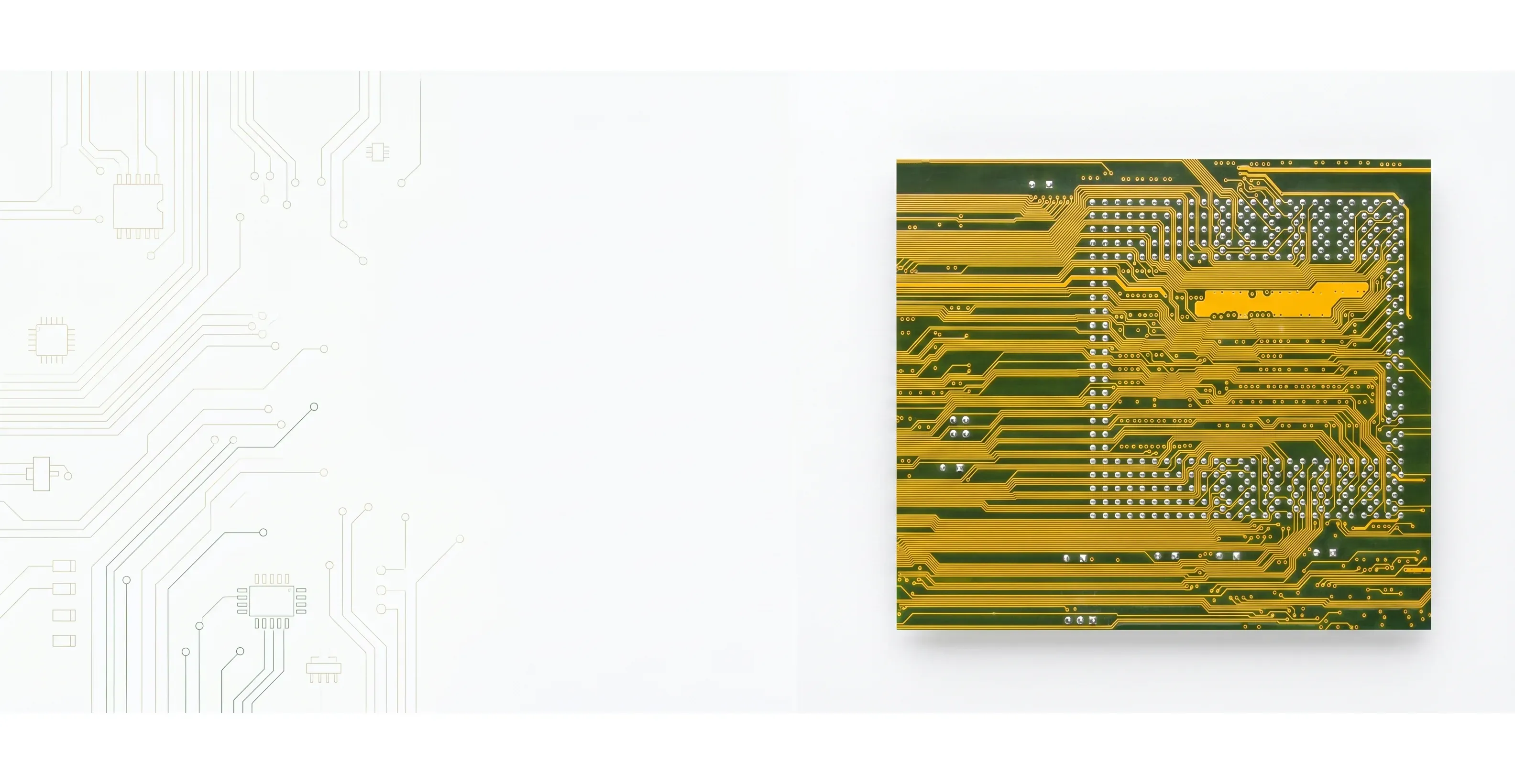
HDI PCB Manufacturing
High Density Interconnect Up to 4-Step Sequential Build
Stacked microvias. Via-in-pad. 3/3mil trace. The routing density you need for next-gen silicon.
At a Glance
HDI Capabilities
From First HDI to Any-Layer
We match your design complexity to the right factory and process.
1-Step (1+N+1)
One laser drill layer per side. Your entry point into HDI: breakout 0.65mm BGA, reduce layer count, enable via-in-pad. 4-24 layers.
2-Step (2+N+2)
Two sequential laminations. Staggered or stacked microvias. For 0.5mm pitch BGA and dense multi-chip modules. 6-24 layers.
3-Step (3+N+3)
Three buildup layers per side. Stacked copper-filled vias. For 0.4mm pitch and maximum via density. 8-14 layers.
4-Step (4+N+4)
Any-layer interconnect capability. Every layer connects to every other through stacked via towers. For the densest designs in mobile and compute. 10-14 layers.
The Difference
Why HDI at AtlasPCB
HDI Done Right
The challenge with HDI isn't whether it can be made — it's whether the microvias will survive thermal cycling. Our factory qualification process ensures long-term reliability.Dedicated HDI Factories
Your HDI board goes to a factory that does HDI every day — not a standard multilayer shop with a laser drill collecting dust.
Stacked Via Expertise
Copper-filled stacked microvias with planarization. Via-in-pad directly under BGA balls without voiding risk.
Stackup Engineering
We verify your via structure feasibility, aspect ratios, and capture pad sizes before production. No surprises.
Microvia Reliability
Process controls for via fill quality, barrel cracking prevention, and thermal cycling reliability. IST testing available.
Applications
Where HDI Makes the Difference
Density Where It Matters
HDI pays for itself when it eliminates layers, shrinks board area, or enables a package that wouldn't route on standard multilayer.Mobile & Wearables
Smartphones, smartwatches, AR glasses — where every 0.1mm of board area matters.
High-Performance Computing
Server CPUs, AI accelerators, FPGA substrates with 0.4mm BGA at 2000+ pins.
Automotive ADAS
Sensor fusion processors, camera modules, lidar control boards in compact housings.
Medical Implants
Miniaturized electronics for hearing aids, neural stimulators, and diagnostic capsules.

FAQ
HDI Questions
Staggered vs stacked microvias?
Staggered: each via offsets from the one below — cheaper, uses more area. Stacked: vias aligned vertically, copper-filled — required for via-in-pad under BGA. Choose stacked when density demands it.
How do I know if I need HDI?
If your BGA pitch is ≤0.65mm, if you need via-in-pad, or if standard routing requires 12+ layers that HDI could do in 8. Upload your design — we will tell you if HDI is necessary or overkill.
What is the lead time?
1-step: 8 days prototype. 2-step: 10-11 days. 3-step: 13-14 days. 4-step: 16-17 days. These are for prototype quantities.
Need HDI?
Upload your design. We'll confirm if HDI is the right approach and which step count you actually need.
Resources
HDI Engineering Guides
Technical deep-dives on HDI design, cost optimization, and manufacturing.
HDI PCB vs Standard Through-Hole: Design Tradeoffs, Cost, and When to Upgrade
Decision framework for choosing between HDI and conventional multilayer construction.
Advanced HDI Stackup Design: Sequential Lamination and ELIC
Deep dive into 1+N+1 through 4+N+4 buildup structures and any-layer interconnect.
Via-in-Pad Design: Filled, Capped, and Plated Over
Complete guide to VIPPO specification for BGA escape routing in HDI boards.
HDI PCB Cost Breakdown and Pricing Guide
Understand what drives HDI pricing and how to optimize your design for cost.
BGA Fanout Routing: Dog-Bone vs Via-in-Pad Breakout
Practical routing strategies for fine-pitch BGA packages on HDI stackups.
Microvia Reliability: Stacked vs Staggered Configurations
IPC-6012 requirements and thermal cycling data for HDI via structures.