· AtlasPCB Engineering · Engineering · 9 min read
HDI PCB vs Standard Through-Hole: Design Tradeoffs, Cost, and When to Upgrade
Comparing HDI PCB technology against standard through-hole construction: routing density, signal integrity, cost per layer, and decision criteria for engineers choosing between conventional and HDI fabrication.
Quick Answer: Standard or HDI?
| Factor | Standard Through-Hole | HDI (Microvia) |
|---|---|---|
| Best for | Pitch > 0.8mm, < 10 layers | Pitch < 0.65mm, density-limited |
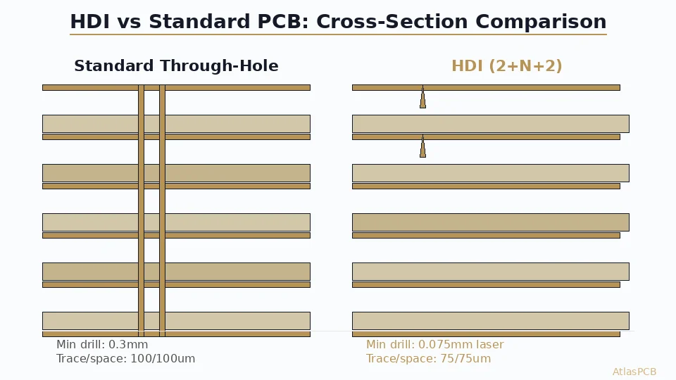
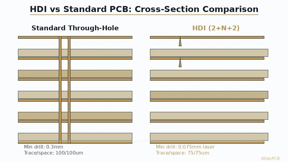
| Min via drill | 0.15mm mechanical | 0.075mm laser |
| Via stub length | Full board thickness | 0.05-0.1mm |
| Trace/space | 100/100um typical | 75/75um or 50/50um |
| Layer count | Up to 30 (practical: 8-16) | Up to 24 HDI |
| Cost multiplier | 1x baseline | 1.5-3x |
| Fabricator availability | 90%+ of fabs | 30-40% of fabs |
| Signal integrity ceiling | Good to ~5 GHz | Excellent to 25+ GHz |
Decision shortcut: If your densest BGA is 0.8mm pitch or above and you can route in 10 layers, stay with standard. If you are fighting for space, using fine-pitch BGAs, or pushing data rates above 10 Gbps, HDI likely saves you layers and improves performance.
The Real Engineering Difference
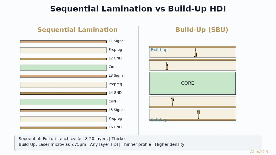
The fundamental distinction between HDI and standard PCB construction comes down to via technology. In standard through-hole boards, every via penetrates the entire board thickness — a 1.6mm board gets a 1.6mm copper barrel whether you need the connection on adjacent layers or across the full stackup. This creates stub resonances that kill signal quality above 5 GHz, wastes routing channels on every layer the via passes through, and forces wider keep-out zones around each drill hit.
HDI replaces this brute-force approach with precision. Laser-drilled microvias connect only the layers they need to reach — typically spanning one or two dielectric layers at 0.05-0.1mm depth. The result is a via structure with negligible stub, minimal parasitic capacitance (0.2-0.3 pF vs 0.8-1.2 pF for through-hole), and a drill diameter small enough to place directly in a BGA pad without dog-bone routing.
This matters most when routing density hits the physical wall. A 0.5mm-pitch BGA with 400 pins requires 20 rows of pads at 0.5mm center-to-center. With standard through-hole vias at 0.3mm drill and 0.5mm pad, you simply cannot fit a via between adjacent pads — the math doesn’t work. HDI microvias at 0.1mm drill with 0.25mm capture pad fit directly inside the BGA land pattern, converting what would require 6+ routing layers into a 2-layer breakout problem.
HDI CAPABILITY
Need HDI for Fine-Pitch BGA Designs?
AtlasPCB builds up to 5+N+5 HDI with stacked microvias, via-in-pad, and 75um trace/space. Our engineers review your BGA fanout strategy before fabrication.
Upload Gerber for HDI Quote ›Signal Integrity: Where HDI Pulls Ahead
The signal integrity advantage of HDI becomes quantifiable at data rates above 5 Gbps. A standard through-hole via in a 1.6mm board creates a stub resonance at approximately 23 GHz (quarter-wavelength of the stub in FR-4), but the signal degradation begins much earlier — insertion loss increases noticeably above 5 GHz, and the via’s parasitic capacitance creates an impedance discontinuity that generates reflections on every high-speed transition.
Backdrilling removes most of the stub in standard boards, bringing effective stub length down to 0.15-0.2mm (limited by drill depth accuracy of +/-3 mil). This extends usable bandwidth to roughly 15 GHz for most applications. However, backdrilling adds cost ($0.02-0.05 per via), requires precise depth control, and still leaves a stub significantly longer than a microvia.
HDI microvias, by contrast, have near-zero stub length inherently. A via-in-pad connection from layer 1 to layer 2 has a total length of 0.06-0.1mm depending on dielectric thickness. At 28 GHz (relevant for 56G PAM4 SerDes), the insertion loss improvement is typically 2-4 dB per via transition compared to a through-hole with backdrilling. For a signal path traversing 4-6 vias, that’s 8-24 dB of margin recovered — often the difference between a passing and failing eye diagram.
The practical implication: designs targeting 25G+ data rates (PCIe Gen 5/6, 400G Ethernet, DDR5+) benefit substantially from HDI construction, not just for density but for electrical performance. Standard through-hole construction requires extensive via optimization (backdrilling, anti-pads, via spacing) to achieve what HDI delivers by default.
SIGNAL INTEGRITY
High-Speed Design Needs Tight Impedance Control?
We manufacture HDI boards with +/-5% impedance tolerance, backdrilling to +/-3mil depth accuracy, and TDR-verified controlled impedance up to 50 GHz test frequency.
Get SI-Optimized Quote ›Cost Comparison: When HDI Actually Saves Money
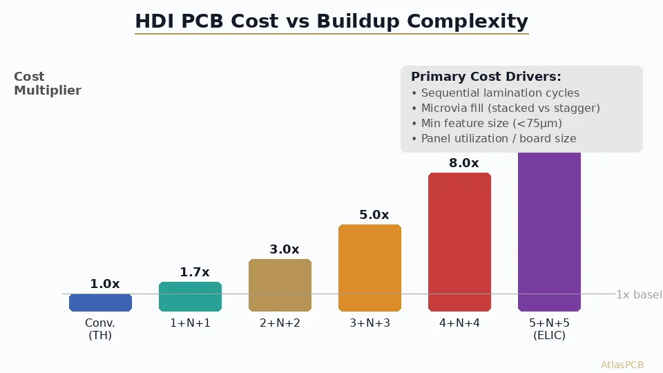
The common assumption that HDI always costs more is incorrect when you factor in the full picture. HDI’s cost premium comes from laser drilling equipment time, sequential lamination cycles (each adds a press cycle), and tighter registration requirements. A simple 1+N+1 build (one microvia layer each side) adds approximately 50-80% to base fabrication cost. A 2+N+2 with stacked vias adds 100-200%.
However, the layer-reduction math often flips the equation. Consider a design that requires 14 layers in conventional construction due to BGA fanout consuming 4 routing layers. The same design in 2+N+2 HDI might achieve identical routing in 10 layers, because microvias free up layer pairs that were previously dedicated to via breakout. The cost comparison becomes:
| Configuration | Layer Count | Approximate Cost (10pcs, 100x100mm) |
|---|---|---|
| Standard 14-layer | 14 | $320-450 |
| HDI 2+N+2 (10-layer core) | 10 | $280-400 |
| Standard 12-layer (if routable) | 12 | $240-340 |
| HDI 1+N+1 (10-layer core) | 10 | $200-300 |
The crossover point typically occurs when HDI eliminates 3+ conventional layers. Below that threshold, standard construction with backdrilling offers better value. The design team’s job is to evaluate whether HDI’s density enables layer reduction — if it does, HDI often wins on both performance and cost.
Board size reduction presents another cost lever. HDI’s higher routing density can shrink a design by 30-50% in area, which translates directly to more boards per panel, lower material consumption, and better panel utilization. For high-volume production (10,000+ units), even a 20% area reduction can offset HDI’s per-board premium through improved panelization efficiency.
COST OPTIMIZATION
Not Sure If HDI Saves You Money?
Upload your design and get a side-by-side quote for standard vs HDI construction. Our engineers identify layer-reduction opportunities that offset the HDI premium.
Reliability Considerations
HDI microvia reliability has been a legitimate concern since the technology’s early days, and the failure modes differ fundamentally from through-hole vias. Standard mechanically-drilled vias fail through barrel cracking under thermal stress — the copper barrel separates at grain boundaries when CTE mismatch between copper and FR-4 generates enough strain. This failure mode is well-understood and addressed through copper thickness specifications (minimum 20um average, 18um minimum per IPC-6012 Class 3).
Microvia failure modes are different. The primary concern is target pad separation — the laser-drilled microvia losing connection to the capture pad on the target layer during thermal cycling. IPC-6012 Rev F addressed this by requiring IST (Interconnect Stress Testing) for HDI structures, with pass criteria of 500+ cycles at current levels generating 150C temperature rise. Stacked microvias (microvia directly on top of another microvia) present higher risk than staggered configurations because thermal stress concentrates at the interface between sequential via fills.
For aerospace and military applications governed by IPC-6012 Class 3 / MIL-PRF-31032, standard through-hole construction still carries a longer qualification heritage and wider acceptance. HDI is gaining ground in these markets — many Tier 1 defense primes now specify HDI for avionics — but qualification cycles are longer and supplier approval more stringent. If your application falls under these requirements, verify your fabricator’s HDI qualification status early in the design process.
Decision Framework
The technology choice comes down to three questions:
First, does your densest component require HDI? If your finest-pitch BGA is 0.5mm or below, HDI is not optional — it’s physically required for breakout. At 0.65mm, HDI is strongly preferred. At 0.8mm and above, standard construction works but HDI may still reduce layers.
Second, does your signal speed demand it? Above 10 Gbps per lane, HDI’s near-zero via stubs provide meaningful SI margin. Below 5 Gbps, standard construction with proper via design suffices. Between 5-10 Gbps, backdrilling in standard construction often bridges the gap.
Third, does the cost math work? Count your conventional layers, identify how many serve primarily as BGA fanout, and estimate the HDI alternative. If HDI eliminates 3+ layers, the economics likely favor it. If layer reduction is 0-2, standard construction with selective backdrilling usually wins.
For most designs in 2026, the industry is converging toward HDI as the default for anything with BGA components below 0.8mm pitch. The fabricator base has matured, costs have decreased 20-30% over the past five years, and reliability data now spans billions of field hours. The question is increasingly not “should I use HDI?” but “what level of HDI complexity does my design actually need?”
ATLASPCB
Ready to Decide? Get Both Quotes in One Request
Upload your Gerber files and we'll provide standard and HDI pricing side by side, with engineering recommendations on the optimal construction for your specific design.
Get Instant Quote ›Related Reading:
About AtlasPCB — We specialize in complex PCB manufacturing for HDI, RF, and high-reliability applications. Explore our HDI PCB manufacturing capabilities, or get an multilayer PCB fabrication up to 30 layers . Every order includes free engineering review. Get your quote.
Reviewed by AtlasPCB Engineering Team — IPC-certified manufacturing specialists with 15+ years of production experience in HDI, RF, and high-reliability PCB fabrication. Content based on factory floor data and real customer design reviews.
- HDI PCB
- through-hole PCB
- microvia
- PCB design
- multilayer PCB
- BGA fanout