· AtlasPCB Engineering · Engineering · 8 min read
BGA Fanout Routing Strategies: Dog-Bone vs Via-in-Pad Breakout for Fine-Pitch Packages
Master BGA fanout routing with detailed strategies for dog-bone and via-in-pad breakout patterns. Covers 0.4mm to 1.27mm pitch BGAs with layer assignment, escape routing, and DFM considerations.
Understanding BGA Fanout Routing
Ball Grid Array (BGA) packages present one of the most challenging routing tasks in PCB design. With hundreds to thousands of solder balls arranged in a dense matrix, engineers must carefully plan how signals escape from beneath the package to reach their destinations on the board.
The fanout strategy—how traces break away from BGA pads to reach routing channels—directly impacts board layer count, manufacturing complexity, signal integrity, and overall project cost. Choosing between dog-bone and via-in-pad approaches is one of the most consequential early decisions in any BGA-heavy design.
This guide provides comprehensive strategies for both approaches, covering pitch ranges from 1.27mm down to 0.4mm, with practical DFM rules and real-world layer assignment examples.
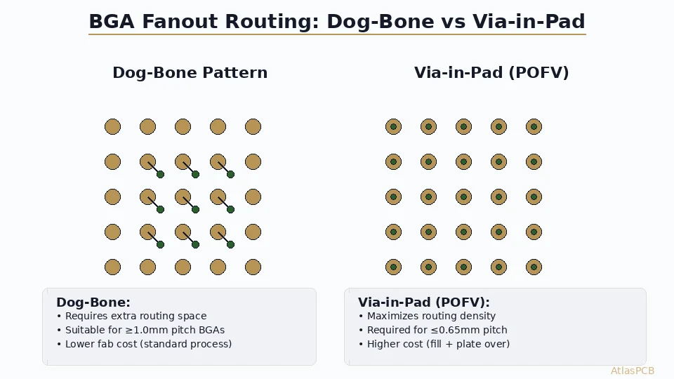
Dog-Bone Fanout: The Standard Approach
Dog-bone fanout places a via adjacent to the BGA pad, connected by a short trace stub. The name comes from the pad-trace-via shape resembling a dog bone when viewed from above.
When to Use Dog-Bone Fanout
Dog-bone routing works effectively for:
- BGA pitch ≥ 0.8mm with standard PCB fabrication (5/5 mil trace/space)
- Prototype and low-volume designs where HDI cost isn’t justified
- Packages with depopulated centers where outer rows can escape on surface layers
- Cost-sensitive designs that need to minimize fabrication complexity
Design Rules for Dog-Bone Patterns
For a standard 1.0mm pitch BGA:
- Pad diameter: 0.5mm (non-solder-mask defined) or 0.45mm (solder-mask defined)
- Via drill: 0.25mm (10 mil)
- Via pad: 0.5mm
- Trace width: 0.1mm (4 mil) connecting pad to via
- Clearance: 0.1mm between via pad and adjacent BGA pad
The critical geometry check: verify that the via pad plus clearance fits within the available space between adjacent BGA pads. For 1.0mm pitch:
Available space = Pitch - Pad diameter = 1.0mm - 0.5mm = 0.5mm
Required = Via pad/2 + Clearance + Pad/2 = 0.25 + 0.1 + 0.25 = 0.6mm
This shows that even at 1.0mm pitch, dog-bone placement requires careful via positioning—typically at 45° angles between pads to maximize clearance.
Escape Routing Strategy by Row
For a typical BGA, escape routing follows a systematic row-by-row approach:
Row 1 (Outer perimeter): Route directly on the top layer, traces exit between pads without vias. This ring provides surface-layer escape for signals, power, and ground.
Row 2: Dog-bone vias drop to Layer 2. Traces route between Row 1 pads on L2, escaping north/south/east/west.
Row 3: Dog-bone vias drop to Layer 3. Signals route on L3 with clearance from L2 routes above.
Row 4+ (Inner rows): Require additional layers or HDI techniques. At 1.0mm pitch, standard dog-bone typically exhausts routing channels after 3-4 rows.
Via Placement Patterns
Four primary via placement orientations exist:
Corner offset (45°): Via placed diagonally between four BGA pads. Most common, maximizes clearance symmetrically.
Inline offset (0°/90°): Via placed directly between two pads in the same row or column. Useful when routing channel direction is predetermined.
Staggered: Alternating via positions between adjacent rows to prevent via-to-via clearance violations.
Grouped: Multiple vias from adjacent pads routed to the same inner layer, used for power/ground consolidation.
Need Expert BGA Routing Support?
AtlasPCB provides DFM review and HDI fabrication for the most demanding BGA designs — from 0.4mm pitch to 2000+ pin packages.
Get a Free DFM Review →Via-in-Pad (POFV): Enabling Ultra-Fine Pitch
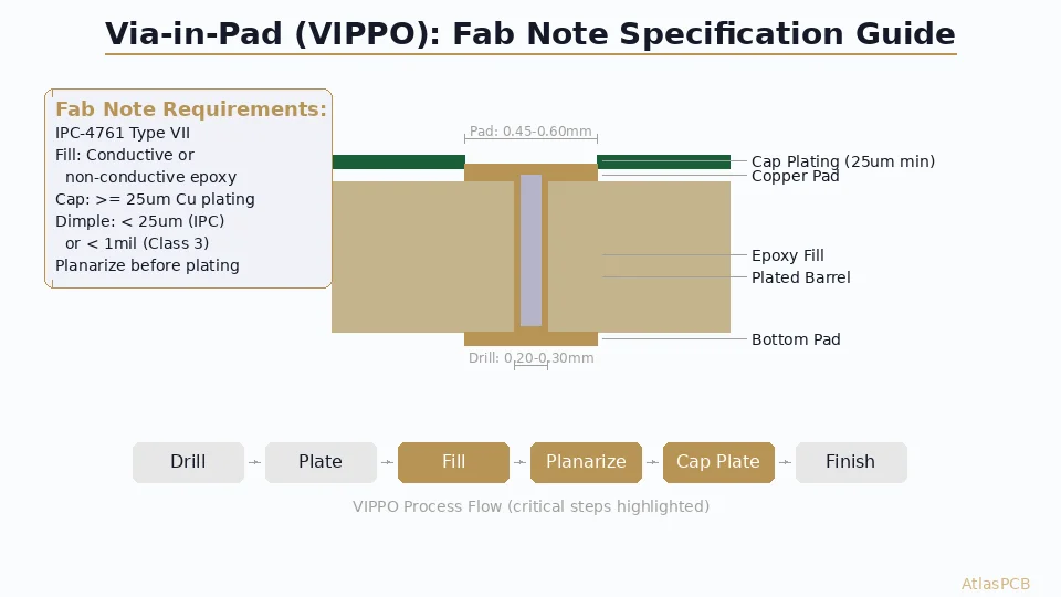
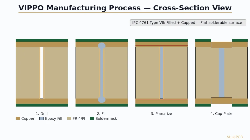
When BGA pitch drops below 0.8mm, there’s simply no room for adjacent vias. Via-in-Pad Plated Over Fill (POFV) solves this by placing the via directly in the center of the BGA pad, filling it with epoxy, and plating it flat for reliable solder joint formation.
Process Steps for Via-in-Pad
- Drill: Laser drill (microvias) or mechanical drill (through-vias) through the pad location
- Plate: Standard electroless + electrolytic copper plating
- Fill: Conductive or non-conductive epoxy fill
- Planarize: Mechanical grinding to achieve flat surface (±10μm)
- Cap plate: Additional copper deposition over filled via
- Surface finish: ENIG, ENEPIG, or other finish applied over capped via
Design Rules for Via-in-Pad
For 0.65mm pitch BGA:
- Pad diameter: 0.35mm (SMD) or 0.30mm
- Via drill: 0.10mm (laser microvia)
- Via capture pad: coincident with BGA pad
- Aspect ratio: ≤0.8:1 for single-layer microvia
For 0.5mm pitch BGA:
- Pad diameter: 0.275mm
- Via drill: 0.075mm (UV laser)
- Stacked or staggered microvias for deeper escape
- HDI 2+N+2 or 3+N+3 stackup required
For 0.4mm pitch BGA:
- Pad diameter: 0.225mm
- Via drill: 0.050mm (advanced UV laser)
- Any-layer HDI (ELIC) often required
- Pad-to-pad clearance: 0.175mm (extremely tight)
HDI Stackup Planning
The layer count for via-in-pad designs depends on pin count and pitch:
| BGA Pitch | Pin Count | Recommended Stackup | Lamination Cycles |
|---|---|---|---|
| 0.65mm | < 300 | 8L (1+N+1) | 1 sequential |
| 0.65mm | 300-600 | 10L (2+N+2) | 2 sequential |
| 0.5mm | < 500 | 10L (2+N+2) | 2 sequential |
| 0.5mm | 500-1000 | 12L (3+N+3) | 3 sequential |
| 0.4mm | Any | 14-16L ELIC | 4+ sequential |
Microvia Reliability Considerations
Stacked microvias (microvia directly on top of another microvia) require careful attention to reliability:
- IPC-2315 guidelines: Maximum 2 stacked microvias without a capture pad reset
- Thermal cycling: Stacked microvias see higher stress than staggered configurations
- Fill quality: Voids in epoxy fill can cause reliability failures during reflow
- Aspect ratio: Keep single-microvia aspect ratio below 0.8:1 for best reliability
For mission-critical designs (aerospace, automotive IATF 16949), prefer staggered microvias over stacked configurations, accepting the additional layer count trade-off for improved long-term reliability.
Layer Assignment Strategy
Effective BGA fanout requires systematic layer assignment to avoid routing congestion:
Signal Escape Layers
- L1 (Top): Outer 1-2 rows escape on surface. Power/ground pads for decoupling caps.
- L2: First inner signal layer. Rows 2-3 escape routes. Preferential routing: horizontal.
- L3: Ground reference plane (critical for impedance control).
- L4: Second inner signal layer. Rows 3-4 escape routes. Preferential routing: vertical.
- L5: Power plane.
- L6-N: Deep escape for center pins, general routing.
Power and Ground Pin Assignment
BGA packages typically have 30-50% power/ground pins. Optimizing their layer assignment:
- Ground pins: Connect directly to ground plane via shortest possible via. Use via-in-pad to minimize inductance.
- Power pins: Route to power plane layer. Group by voltage rail and provide local decoupling.
- Thermal pads: If present, connect to internal copper plane with multiple vias for heat spreading.
DFM Considerations for Manufacturing
Solder Joint Reliability
Dog-bone fanout can cause solder wicking if the via isn’t properly tented or plugged. Solder flows down the via barrel during reflow, starving the joint. Solutions:
- Via tenting: Apply solder mask over via on component side
- Via plugging: Fill with mask ink (less reliable than POFV)
- Via-in-pad: Eliminates wicking entirely (recommended for BGA)
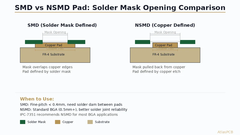
Pad Definition Method
Two approaches for BGA pad definition:
Non-Solder-Mask Defined (NSMD): Copper pad smaller than mask opening. Provides better solder joint fatigue life (fillet wraps around pad edges). Preferred for most applications.
Solder-Mask Defined (SMD): Mask opening smaller than copper pad. Better for very fine-pitch where mask registration is critical. Reduces effective pad size.
For pitches ≤0.5mm, SMD pads are often necessary due to solder mask registration tolerances (±25μm typical).
Testability Planning
Consider ICT (In-Circuit Test) access during fanout design:
- Reserve test point pads on inner signal layers for critical nets
- Provide accessible test pads on board edges for key BGA signals
- Plan boundary-scan (JTAG) chain routing early to avoid last-minute routing conflicts
Routing Channel Calculation
The number of traces that can pass between adjacent BGA vias/pads determines routing feasibility:
Channels = floor((Pitch - Pad - 2×Clearance) / (TraceWidth + Space))For 1.0mm pitch, 0.5mm pad, 0.1mm clearance, 0.1/0.1mm trace/space:
Channels = floor((1.0 - 0.5 - 0.2) / 0.2) = floor(1.5) = 1One trace per channel between pads. This means inner rows of a 1.0mm BGA can only escape one signal per channel per layer—directly driving the layer count requirement.
For 0.8mm pitch:
Channels = floor((0.8 - 0.45 - 0.2) / 0.2) = floor(0.75) = 0Zero routing channels between pads at 0.8mm with 4-mil rules—this is exactly why HDI becomes mandatory below 0.8mm pitch.
Practical Example: 676-Pin FPGA at 1.0mm Pitch
Consider a Xilinx/AMD Artix-7 in FG676 package (26×26 matrix, 1.0mm pitch):
Layer count estimation:
- Outer 2 rows: 200 pins escape on L1 (top)
- Rows 3-4: ~150 pins escape on L2 (via dog-bone)
- Rows 5-6: ~120 pins escape on L4
- Rows 7-13 (center): ~200 pins need L6+ or HDI
Recommended stackup: 10-layer (if many center pins are power/ground) or 12-layer (if high signal density in center).
Design flow:
- Assign power/ground pins first—drop to respective planes
- Route critical signals (clocks, high-speed SerDes) on preferred layers
- General I/O signals fill remaining routing channels
- Verify timing/length matching on escaped traces before committing
Signal Integrity Impact
BGA via transitions affect signal integrity through:
Via Stub Resonance
A through-hole via under a BGA creates a stub from the signal layer to the board bottom. At high frequencies, this stub resonates:
f_resonance = c / (4 × stub_length × √εr)For a 1.6mm board with signal on L2 (0.2mm depth), stub = 1.4mm:
f = 3×10⁸ / (4 × 0.0014 × √4.2) = ~26 GHzFor signals above 10 Gbps (NRZ), back-drilling the via stub is recommended to maintain channel performance.
Via Inductance and Capacitance
Microvia inductance is significantly lower than through-hole via:
- Through-hole via (1.6mm length): ~0.8 nH
- Microvia (0.1mm depth): ~0.05 nH
For power delivery networks, lower via inductance directly reduces voltage droop during transient current demands.
Cost Comparison and Decision Matrix
| Factor | Dog-Bone | Via-in-Pad (POFV) |
|---|---|---|
| Fab cost (per board) | Baseline | +15-30% |
| Layer count needed | Higher (+2-4 layers) | Lower |
| Board area | Larger | Compact |
| Signal integrity | Good (standard speeds) | Excellent (high-speed) |
| Thermal performance | Moderate | Better (direct thermal path) |
| Suitable pitch | ≥0.8mm | ≤0.8mm |
| Solder reliability | Needs via tenting | Inherently reliable |
| Lead time | Standard | +3-5 days |
Further Reading
- Via-in-Pad Plated Over Design Guide
- BGA X-Ray Void Analysis per IPC-7095
- HDI PCB Stackup Design for Advanced Applications
- Fine-Pitch BGA DFM Design Rules
Ready to tackle your next fine-pitch BGA design? Our engineering team reviews complex BGA fanout routability before fabrication to ensure first-pass success. Request a DFM consultation →
About AtlasPCB — We specialize in complex PCB manufacturing for HDI, RF, and high-reliability applications. Explore our HDI PCB manufacturing capabilities . Every order includes free engineering review. Get your quote.
Reviewed by AtlasPCB Engineering Team — IPC-certified manufacturing specialists with 15+ years of production experience in HDI, RF, and high-reliability PCB fabrication. Content based on factory floor data and real customer design reviews.
- BGA
- fanout routing
- via-in-pad
- dog-bone
- PCB layout
- fine-pitch
- HDI
- routing strategy
- breakout