· AtlasPCB Engineering · Engineering · 6 min read
BGA X-Ray Void Analysis: IPC-7095 Acceptance Criteria and Inspection Best Practices
Master BGA solder joint void analysis using X-ray inspection. Understand IPC-7095 acceptance criteria, void percentage calculations, and how to distinguish process voids from reliability-threatening defects.

Why BGA Void Analysis Matters
Ball Grid Array (BGA) packages dominate modern PCB assembly — from mobile processors to automotive ECUs and networking ASICs. Unlike leaded components where solder joints are visually inspectable, BGA connections are hidden beneath the package body. X-ray inspection is the only non-destructive method to evaluate BGA solder joint quality.
Voids — gas pockets trapped within solder joints — are the most common BGA anomaly detected during X-ray inspection. Understanding when voids represent a genuine reliability risk versus an acceptable process artifact is critical for yield optimization and quality decisions.
Understanding IPC-7095: The BGA Standard
IPC-7095 “Design and Assembly Process Implementation for BGAs” provides the industry-standard framework for BGA void acceptance. The key sections addressing voids are:
Void Classification by Size
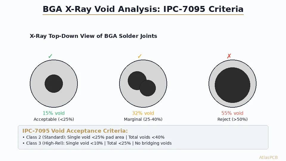
IPC-7095 defines void percentage as:
Void% = (Sum of void areas / Pad area) × 100
Where pad area is the designed copper pad area (not the solder ball diameter).
Class 2 (Standard Electronic Products)
- Individual void: ≤25% of pad area
- Total voiding: ≤40% of pad area (sum of all voids)
- No single void touching both pad interfaces (top and bottom)
- Applications: Consumer electronics, commercial computing, telecom
Class 3 (High-Reliability Products)
- Individual void: ≤10% of pad area
- Total voiding: ≤25% of pad area
- No voids at pad-to-solder interface (interface voids are more critical)
- No voiding that creates a continuous path across the joint
- Applications: Aerospace, medical devices, military, automotive safety
Process Indicator Levels
Beyond pass/fail, IPC-7095 establishes process control levels:
| Level | Total Void % | Action Required |
|---|---|---|
| Target | <10% | Normal production |
| Acceptable | <25% (Class 3) / <40% (Class 2) | Monitor trend |
| Process Alert | 25-40% (Class 3) / 40-50% (Class 2) | Investigation needed |
| Reject | >40% (Class 3) / >50% (Class 2) | Rework or scrap |
X-Ray Inspection Methodology
2D Transmission X-Ray
The standard inspection method for production BGA void analysis:
Equipment requirements:
- Tube voltage: 90-130 kV (dependent on board thickness)
- Geometric magnification: 10-50×
- Detector resolution: ≤5 μm feature size
- Oblique angle capability: 0-70° tilt for layer separation
Measurement procedure:
- Acquire top-down (0°) image of BGA area
- Identify solder ball boundaries using grayscale thresholding
- Calculate pad area (circle fit or actual pad geometry)
- Identify voids as darker regions within ball area
- Calculate individual and total void percentages
- Compare against IPC-7095 class requirements
Oblique Angle Inspection
Tilting the X-ray beam to 30-60° separates overlapping features:
- 30° tilt: Separates top and bottom BGA rows in double-sided assemblies
- 45° tilt: Reveals head-in-pillow (HIP) defects hidden in 0° view
- 60° tilt: Exposes non-wetting conditions and collapsed/bridged balls
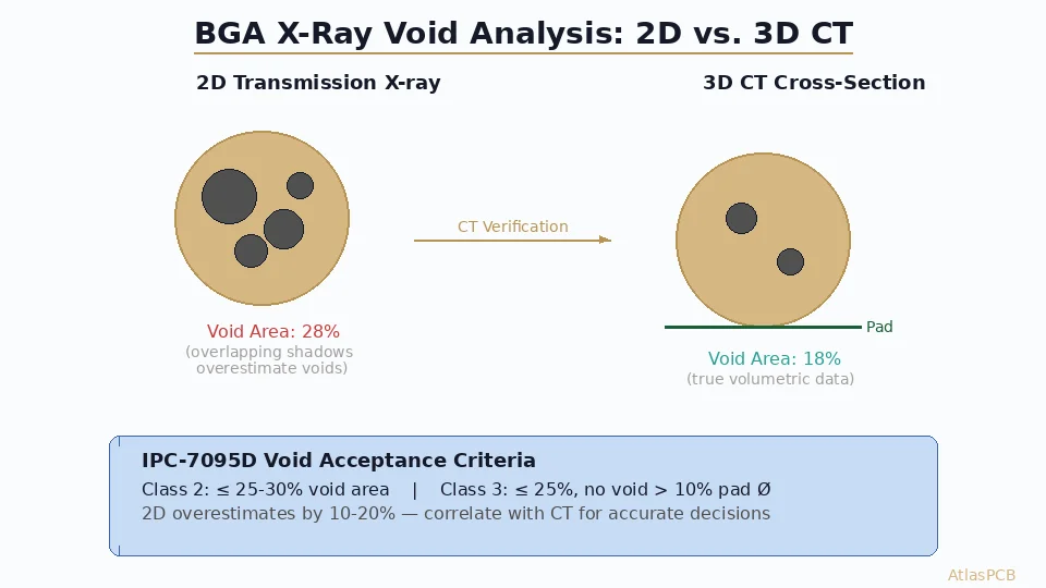
3D CT (Computed Tomography)
For failure analysis and critical reliability assessment:
- Creates full 3D volumetric reconstruction
- Reveals void position within joint (interface vs bulk)
- Identifies crack propagation paths post-thermal cycling
- Resolution: 1-5 μm voxel size (micro-CT)
- Throughput: 5-30 minutes per component (not suitable for 100% inspection)
Need Production BGA Assembly with X-Ray Inspection?
AtlasPCB's assembly line includes 5DX automated X-ray inspection with 100% BGA coverage. We provide void analysis reports meeting IPC-7095 Class 2/3 requirements.
Request Assembly Quote →Root Cause Analysis: Why Voids Form
Flux Outgassing (Most Common — 60-70% of Cases)
During reflow, flux activators and vehicles decompose and release gases. If the solder solidifies before these gases escape, voids remain trapped.
Contributing factors:
- Aggressive ramp rate (>2°C/sec) — insufficient time for flux activation
- Short time above liquidus (<60 sec for SAC305)
- Excessive flux volume (stencil too thick or aperture oversized)
- Low-activity flux unable to fully activate at process temperature
Mitigation:
- Optimize reflow profile: Extend soak zone (150-200°C) to 60-90 seconds
- Ensure TAL (time above liquidus) ≥ 60 seconds for SAC alloys
- Consider vacuum reflow for critical applications (reduces voids to <2%)
Moisture-Related Voiding
Moisture absorbed in PCB laminate or BGA substrate explosively vaporizes during reflow:
- FR-4 absorbs 0.1-0.3% moisture by weight
- BGA substrates (especially organic) absorb 0.05-0.15%
- At 250°C, trapped moisture generates ~20 atm pressure
Mitigation:
- Bake PCBs at 125°C for 4-8 hours before assembly
- Handle BGAs per MSL (Moisture Sensitivity Level) requirements
- Monitor factory humidity (<60% RH in assembly areas)
Via-in-Pad Voiding
When vias beneath BGA pads are not properly filled and capped:
- Solder wicks into via barrel during reflow
- Air trapped in via creates large void directly at interface
- Most critical void type — directly impacts thermal path
Mitigation:
- Specify VIPPO (Via-In-Pad Plated Over) with 100% copper fill
- Verify via fill by cross-section (target >95% fill)
- Alternative: Use dog-bone fanout to avoid via-in-pad
Pad Surface Contamination
Oxidation, organic contamination, or plating defects on pads:
- ENIG black pad (nickel hyper-corrosion) causes widespread non-wetting
- OSP shelf life exceeded (>6 months) leads to oxidation
- Solder mask residue on pad edges traps flux
Automated vs Manual Void Measurement
Automated X-Ray Inspection (AXI)
Modern AXI systems provide:
- Throughput: 100% inspection at line speed (5-15 sec/board)
- Consistency: Algorithmic void calculation eliminates operator variability
- Statistics: SPC data for trend monitoring across production lots
- Limitations: 2D measurement may overestimate void % when voids overlap vertically
Manual Measurement Best Practices
For failure analysis and arbitration:
- Use calibrated measurement software (not estimated percentages)
- Define ball boundary using 50% grayscale threshold
- Define void boundary using same threshold method
- Calculate area using pixel counting, not diameter estimation
- Document measurement parameters for reproducibility
Process Optimization: Reducing BGA Voids
Reflow Profile Optimization
The single most effective lever for void reduction:
| Profile Parameter | Void-Prone | Optimized |
|---|---|---|
| Ramp rate | >2.5°C/s | 1.0-1.5°C/s |
| Soak time (150-200°C) | <30 sec | 60-90 sec |
| Time above liquidus | <45 sec | 60-90 sec |
| Peak temperature | >250°C | 240-245°C (SAC305) |
| Cooling rate | >4°C/s | 2-3°C/s |
Stencil Design Impact
- Aperture reduction: 1:1 pad-to-aperture for 0.5 mm pitch; 90% for larger pitches
- Stencil thickness: 100-125 μm for fine-pitch BGA; 150 μm for 1.0+ mm pitch
- Aperture shape: Round apertures produce fewer voids than square for BGA sites
- Nano-coating: Reduces flux sticking and improves paste release
Advanced Solutions
- Vacuum reflow: Reduces voids to <2% by evacuating chamber at peak temperature
- Nitrogen atmosphere: Prevents oxidation, allowing lower peak temperatures
- Formic acid reflow: Eliminates flux entirely for ultra-low void applications
Industry Trends: Evolving Void Challenges
Package-on-Package (PoP) and 3D Stacking
Stacked packages create multiple solder layers, making void detection more complex:
- Overlapping ball images require CT or oblique angle separation
- Thermal path through multiple joints amplifies void impact
- Industry moving toward stricter <15% total void for PoP applications
Fine-Pitch BGA (≤0.4 mm)
Smaller balls have proportionally larger surface-area-to-volume ratios:
- Flux outgassing has less solder mass to escape through
- Via-in-pad becomes mandatory, increasing void risk
- Void percentage thresholds may need revision for sub-0.4mm pitch
Further Reading
- BGA Pad Design and Via-in-Pad Solder Voiding Prevention
- AOI and SPI Inspection in PCB Assembly Quality Control
- DFM Rules for Fine-Pitch BGA PCB Design
Ensure Quality BGA Assembly with AtlasPCB
Our assembly facility features automated X-ray inspection with IPC-7095 void analysis capability, vacuum reflow for critical applications, and comprehensive SPC monitoring. Whether you need Class 2 production volumes or Class 3 aerospace-grade quality, our process engineering team optimizes every parameter for your specific BGA requirements.
About AtlasPCB — We specialize in complex PCB manufacturing for HDI, RF, and high-reliability applications. Explore our HDI PCB manufacturing capabilities, PCB assembly services, or get an full PCB manufacturing capabilities . Every order includes free engineering review. Get your quote.
Reviewed by AtlasPCB Engineering Team — IPC-certified manufacturing specialists with 15+ years of production experience in HDI, RF, and high-reliability PCB fabrication. Content based on factory floor data and real customer design reviews.
- bga
- x-ray inspection
- void analysis
- ipc-7095
- solder joint
- pcb assembly
- quality control