· AtlasPCB Engineering · Engineering · 12 min read
Via-in-Pad Plated Over (VIPPO) Design Guide
Complete guide to VIPPO technology covering via fill, copper capping, BGA fanout design rules, and manufacturing process steps.
What Is Via-in-Pad Plated Over (VIPPO)?
Via-in-Pad Plated Over—commonly abbreviated VIPPO—is a PCB fabrication technique in which a plated through-hole or microvia is drilled directly into the surface mount pad, filled with material, capped with copper, and planarized flat. The result is a component pad that looks and behaves like a standard SMD pad while hiding a vertical interconnect beneath it.
The technique solves a fundamental routing problem: as BGA pitch shrinks below 0.8 mm, there is no room between pads for conventional dog-bone fanout traces. VIPPO eliminates the fanout entirely by routing the signal straight down through the pad. This article covers the complete design-to-fabrication workflow, IPC specifications, fill material choices, design rules, and common failure modes.
If you are designing high-density boards with fine-pitch components, understanding VIPPO is not optional—it is essential. For a broader look at high-density interconnect structures, see our overview of [HDI PCB technology]/blog/hdi-pcb-technology/).
Why VIPPO Exists: The BGA Routing Problem
Modern ICs—FPGAs, SoCs, network processors—use ball grid arrays with pitches of 1.0 mm, 0.8 mm, 0.65 mm, 0.5 mm, and even 0.4 mm. At 1.0 mm pitch, there is enough space between pads to route one trace (dog-bone fanout). At 0.65 mm pitch and below, even a single trace between pads becomes impossible with standard manufacturing tolerances.
Pitch vs. Routing Space
| BGA Pitch (mm) | Pad Diameter (mm) | Gap Between Pads (mm) | Dog-Bone Feasible? | VIPPO Required? |
|---|---|---|---|---|
| 1.27 | 0.60 | 0.67 | Yes (2 traces) | No |
| 1.00 | 0.50 | 0.50 | Yes (1 trace) | Optional |
| 0.80 | 0.40 | 0.40 | Marginal | Recommended |
| 0.65 | 0.35 | 0.30 | No | Yes |
| 0.50 | 0.25 | 0.25 | No | Yes |
| 0.40 | 0.20 | 0.20 | No | Yes |
Without VIPPO, the only alternative at fine pitch is to use blind or buried microvias offset from the pad—but this still requires a short trace from pad to via, consuming precious routing space and adding inductance. VIPPO places the via at the geometric center of the pad, achieving the shortest possible vertical interconnect and the maximum routing density.
For pad geometry guidelines specific to BGA and QFN packages, refer to our [PCB pad design for BGA and QFN]/blog/pcb-pad-design-bga-qfn/) guide.
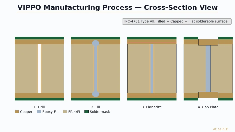
The VIPPO Manufacturing Process
VIPPO fabrication adds several process steps compared to standard PCB manufacturing. Understanding the sequence is critical for creating designs that your fabricator can actually build.
Step 1: Drilling
The via is drilled through the copper-clad laminate. Two methods are used:
- Mechanical drilling — For through-hole VIPPO vias with diameters ≥ 0.20 mm. Standard carbide drill bits. Maximum aspect ratio of about 10:1 for reliable plating.
- Laser drilling — For blind microvias in HDI stackups with diameters of 0.075–0.15 mm. CO₂ or UV-YAG lasers. Maximum depth-to-diameter aspect ratio of approximately 0.8:1 to 1:1.
For a deep dive into laser drilling parameters, see [Laser drilling and microvia technology]/blog/pcb-laser-drilling-microvia-technology/).
Step 2: Plating the Barrel
The drilled hole is desmeared (for laser vias, plasma or permanganate desmear removes resin residue) and then electrolessly seeded with copper, followed by electrolytic copper plating to build up the barrel wall. Typical barrel plating thickness is 20–25 µm.
Step 3: Via Fill
The plated via is filled. This is the step that distinguishes VIPPO from a simple via-in-pad. Three fill materials are commonly used:
| Fill Type | Material | Thermal Conductivity (W/m·K) | CTE (ppm/°C) | Cost | Best For |
|---|---|---|---|---|---|
| Non-conductive epoxy | Silver-free epoxy paste | 0.5–2.0 | 30–50 | Low | General signal vias |
| Conductive epoxy | Silver-filled epoxy | 3.0–15.0 | 25–40 | Medium | Moderate thermal vias |
| Electrochemical copper | Electrolytic Cu fill | 385 | 17 | High | High-current / thermal vias |
Non-conductive epoxy fill (IPC-4761 Type VII) is the most common. The epoxy is screen-printed or pressure-injected into the via, then cured at 150–170 °C. After curing, the surface is planarized by belt sanding or ceramic lapping to remove any epoxy proud of the copper surface.
Conductive epoxy fill uses silver-particle-loaded paste. It provides some thermal benefit but should not be confused with solid copper—the thermal conductivity is typically only 3–15 W/m·K versus 385 W/m·K for solid copper.
Electrochemical copper fill deposits solid copper into the via barrel using specialized plating chemistry (pulse-reverse plating with suppressor/accelerator additives). This produces a nearly void-free solid copper column and is the gold standard for thermal vias under power components. The downside is cost and cycle time—fill plating can take 2–4 hours per panel.
Step 4: Planarization
After filling, the panel surface is ground flat using ceramic or diamond-grit belt sanders. The goal is a surface co-planarity of ≤ 5 µm across the filled via and surrounding copper. This is critical—any dimple or bump will cause solder paste printing defects during assembly.
Step 5: Cap Plating
A final copper plating step deposits 15–25 µm of copper over the planarized fill and the surrounding pad copper. This “cap” seals the fill material and creates a continuous copper surface that accepts surface finish (ENIG, HASL, OSP, etc.) uniformly.
Step 6: Outer Layer Imaging and Etching
Standard photolithography defines the pad geometry. The VIPPO pad is now indistinguishable from a normal SMD pad—flat, uniform copper, with fill material sealed beneath the cap.
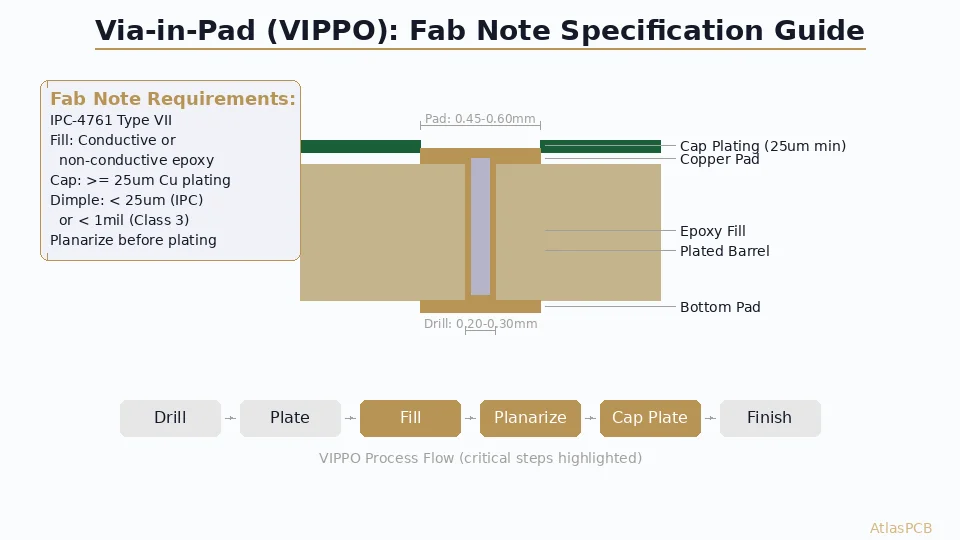
IPC Standards for Via Fill and VIPPO
The IPC-4761 standard defines seven types of via protection. VIPPO corresponds to Type VII: Filled and capped (plated over). Key requirements:
| Parameter | IPC-4761 Type VII Requirement |
|---|---|
| Fill void | ≤ 50% of via depth (Class 2), ≤ 25% (Class 3) |
| Dimple/protrusion | ≤ 75 µm (Class 2), ≤ 50 µm (Class 3) |
| Cap plating thickness | ≥ 12 µm over filled via |
| Surface co-planarity | ≤ 25 µm across pad |
IPC-6012 Class 3 (high-reliability) imposes tighter constraints on fill voids and co-planarity. If your product targets aerospace, medical, or automotive applications, specify Class 3 requirements explicitly on your fabrication drawing.
Design Rules for VIPPO
Via Size and Aspect Ratio
The most common mistake in VIPPO design is specifying vias that are too small to fill reliably or that have excessive aspect ratios.
Mechanically drilled VIPPO vias:
| Parameter | Recommended | Minimum (Advanced) |
|---|---|---|
| Finished hole diameter | 0.25–0.30 mm | 0.20 mm |
| Maximum board thickness for fill | 2.0 mm | 1.6 mm |
| Aspect ratio (depth:diameter) | ≤ 8:1 | 10:1 |
| Annular ring | ≥ 0.10 mm | 0.075 mm |
| Pad diameter | Hole + 0.30 mm | Hole + 0.20 mm |
Laser-drilled microvia VIPPO (HDI):
| Parameter | Recommended | Minimum (Advanced) |
|---|---|---|
| Top diameter | 0.10–0.15 mm | 0.075 mm |
| Bottom diameter (capture pad) | 0.08–0.12 mm | 0.060 mm |
| Depth (single dielectric layer) | 0.065–0.10 mm | 0.050 mm |
| Aspect ratio | ≤ 0.8:1 | 1:1 |
| Capture pad diameter | ≥ 0.25 mm | 0.20 mm |
Pad Design for VIPPO
The pad diameter must accommodate the via drill, the annular ring, and registration tolerances. A general formula:
Pad diameter = Via drill diameter + (2 × annular ring) + registration tolerance
For a 0.25 mm drill with 0.10 mm annular ring and 0.05 mm registration tolerance:
Pad = 0.25 + 0.20 + 0.05 = 0.50 mm
This matches the standard NSMD pad for a 0.8 mm pitch BGA—confirming that VIPPO is geometrically compatible with the component footprint without pad enlargement.
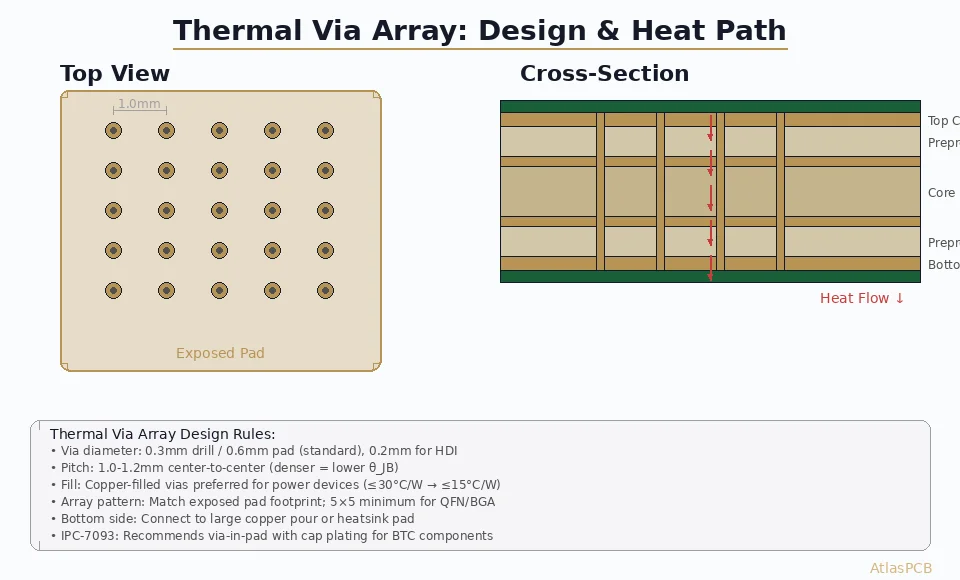
Thermal Via Arrays
For power pads (exposed thermal pads on QFNs, power MOSFETs, etc.), VIPPO thermal via arrays provide the lowest thermal resistance path from pad to internal or bottom copper planes.
Design guidelines for thermal via arrays:
- Via pitch: 1.0–1.2 mm (center to center)
- Via diameter: 0.30 mm finished hole
- Fill: Electrochemical copper for best performance; conductive epoxy for cost savings
- Array should cover ≥ 60% of the thermal pad area
- Connect all thermal vias to a continuous copper plane on the opposite side
Thermal resistance comparison (per via, 1.6 mm board):
| Via Fill | Thermal Resistance per Via (°C/W) |
|---|---|
| Open (air-filled) | ~120 |
| Non-conductive epoxy | ~80 |
| Conductive epoxy | ~35 |
| Solid copper (electrochemical) | ~8 |
The difference between an open via and a copper-filled via is an order of magnitude—this matters enormously for components dissipating more than 1–2 W.
BGA Fanout Strategies with VIPPO
Full-Matrix VIPPO (All Balls Via-in-Pad)
Every BGA ball has a VIPPO via beneath it. This is the most aggressive approach and enables routing of all signals to inner layers without any surface traces between pads. Required for ≤ 0.5 mm pitch BGAs with full pin utilization.
Stackup implications: Full-matrix VIPPO on fine-pitch BGAs typically requires an HDI stackup with at least 1+N+1 buildup (one microvia layer each side). For 0.4 mm pitch with high I/O count, 2+N+2 or even 3+N+3 may be necessary.
Peripheral VIPPO with Inner Dog-Bone
For 0.8–1.0 mm pitch BGAs, the inner rows use VIPPO while the outer two rows use conventional dog-bone fanout. This hybrid approach reduces cost by limiting the number of filled vias while still enabling escape routing for the inner ball field.
Via-in-Pad for Decoupling Capacitors
VIPPO is not just for BGAs. Placing decoupling capacitors with via-in-pad connections directly to power/ground planes minimizes the loop inductance of the decoupling path. For 0402 and 0201 capacitors in high-speed designs (> 5 GHz), this technique can reduce parasitic inductance from ~1 nH (dog-bone fanout) to ~0.3 nH (VIPPO direct).
For more on via-in-pad applications and general guidelines, see our [Via-in-pad design guide]/blog/via-in-pad-design/).
Common VIPPO Defects and How to Avoid Them
Solder Void from Incomplete Fill
If the via fill contains a void near the pad surface, solder can wick into the void during reflow, starving the joint. This is the number-one VIPPO failure mode.
Prevention:
- Specify IPC-4761 Type VII with Class 3 void requirements (≤ 25% void)
- Request cross-section validation on first articles
- Avoid aspect ratios above 8:1 for mechanically drilled vias
Dimple or Protrusion at Pad Surface
Incomplete planarization leaves a concave dimple or convex bump. Dimples cause solder paste to pool unevenly; protrusions cause tombstoning on small passives.
Prevention:
- Specify surface co-planarity ≤ 25 µm
- Use automated optical inspection (AOI) post-planarization
Cracked Fill After Thermal Cycling
CTE mismatch between the fill material and the surrounding copper/laminate can cause fill cracking during thermal excursion. This is primarily a concern for non-conductive epoxy fills in thick boards (> 2.0 mm).
Prevention:
- Use conductive or copper fill for boards > 2.0 mm
- Specify fill materials with CTE ≤ 35 ppm/°C
- Validate with thermal cycling qualification (IPC-TM-650 2.6.26)
Cap Plating Delamination
Poor adhesion between the copper cap and the fill surface causes delamination, especially if the planarized fill surface is contaminated or over-cured.
Prevention:
- Micro-etch or chemical treatment of fill surface before cap plating
- Control epoxy cure profile to manufacturer specifications
- Pull-strength testing on first articles
Cost Impact of VIPPO
VIPPO adds cost. Understanding where the cost comes from helps you make informed design trade-offs.
| Process Step | Additional Cost vs. Standard Via |
|---|---|
| Via fill (non-conductive epoxy) | +15–25% per via |
| Via fill (conductive epoxy) | +25–40% per via |
| Via fill (electrochemical copper) | +50–80% per via |
| Planarization | +10–15% panel processing |
| Cap plating | +5–10% panel processing |
| Total board cost impact | +8–30% depending on via count and fill type |
For a 6-layer board with 200 VIPPO vias using non-conductive epoxy fill, expect roughly a 10–15% cost premium over the same board with conventional dog-bone routing. For an 8-layer HDI with 1,000+ copper-filled VIPPO vias, the premium can reach 25–30%.
The cost is justified when VIPPO enables a layer count reduction (e.g., routing a design in 8 layers with VIPPO that would otherwise require 10 layers) or when thermal/electrical performance requirements demand it.
Design Checklist for VIPPO
Before sending your design to fabrication, verify these items:
- Via size and aspect ratio within fabricator capability (request their VIPPO capability table)
- Fill material specified on fab drawing (non-conductive, conductive, or copper)
- IPC-4761 Type VII called out with class level (Class 2 or 3)
- Co-planarity requirement specified (≤ 25 µm recommended)
- Annular ring meets minimum (≥ 0.075 mm for advanced, ≥ 0.10 mm standard)
- Thermal vias connected to continuous planes, not isolated pads
- Solder mask does not cover VIPPO pads (NSMD preferred for BGA)
- Surface finish compatible with VIPPO pads (ENIG, ENEPIG, or OSP recommended)
- Cross-section requirement on first article for fill void and co-planarity verification
- Impedance-controlled vias have correct pad/antipad sizing in reference planes
For a comprehensive pre-fabrication review, use our [PCB DFM checklist]/blog/pcb-dfm-checklist/).
When Not to Use VIPPO
VIPPO is not always the right answer. Avoid it when:
- BGA pitch is ≥ 1.0 mm and dog-bone fanout provides sufficient routing — VIPPO adds cost without benefit
- Via count is low (< 20 filled vias) — the setup cost for via fill may exceed the benefit
- Board thickness exceeds 3.0 mm — mechanically drilled via fill becomes unreliable at high aspect ratios
- Prototype speed is critical — VIPPO adds 2–5 days to standard lead times; via-in-pad with solder mask tenting (IPC-4761 Type V) may be an acceptable quick-turn alternative, though with solder voiding risk
VIPPO in HDI Stackups
In HDI designs, VIPPO is almost always used for microvias. The typical HDI flow is:
- Fabricate core layers with PTH vias (standard or filled)
- Laminate buildup dielectric layers
- Laser drill microvias through buildup layers
- Plate microvia barrels
- Fill microvias (usually electrochemical copper for stacked vias)
- Planarize and cap plate
- Image and etch outer layers
Stacked vs. staggered microvias: Copper-filled VIPPO microvias can be stacked directly on top of each other across multiple buildup layers (e.g., in a 2+N+2 stackup, the Layer 1→2 via sits directly on the Layer 2→3 via). This requires copper fill—epoxy fill cannot support the mechanical load of stacking. Staggered microvias (offset from each other) can use epoxy fill.
For a full treatment of HDI stackup design and microvia rules, see [HDI PCB technology]/blog/hdi-pcb-technology/).
Signal Integrity Considerations
VIPPO vias offer signal integrity advantages beyond just routing density:
- Lower inductance — The via stub is eliminated when the via connects only the pad layer to the first inner layer (blind via). For through-hole VIPPO, back-drilling can remove the stub.
- Controlled impedance — The filled via barrel has a more predictable impedance than an air-filled barrel, though the difference is small for signal vias.
- Reduced crosstalk — Tighter BGA fanout means shorter parallel trace runs between pads, reducing near-end crosstalk.
For designs operating above 10 Gbps, combine VIPPO with back-drilling or blind vias to minimize stub resonance. The stub resonance frequency for a 1.0 mm stub in FR-4 is approximately 37 GHz—problematic for 28G and 56G SerDes but acceptable for most applications below 10 Gbps.
Conclusion and Next Steps
VIPPO is the enabling technology for modern high-density PCB design. It allows direct vertical interconnect beneath fine-pitch BGAs, maximizes routing density, improves thermal performance, and supports signal integrity at multi-gigabit data rates. The trade-off is increased fabrication cost and lead time, along with tighter process controls that demand a capable manufacturer.
When specifying VIPPO, communicate clearly with your fabricator: call out IPC-4761 Type VII, specify the fill material, define co-planarity requirements, and request first-article cross-sections. A few well-placed notes on your fab drawing prevent the most common VIPPO failures.
Ready to implement VIPPO in your next design? Upload your Gerbers for a free engineering review and our team will verify your via fill specifications, check aspect ratios, and confirm manufacturability before production begins.
Further Reading
- [BGA Pad Design and Via-in-Pad: How to Prevent Solder Voiding in High Pin-Count BGA Assemblies]/blog/bga-pad-design-via-in-pad-solder-voiding-prevention/)
- [Via-in-Pad Design: Filled, Capped, and Plated Over — Complete Guide]/blog/via-in-pad-design/)
- [PCB Thermal Management: Heat Dissipation Techniques for Reliable Electronics]/blog/pcb-thermal-management/)
- [Press-Fit Via Design for PCB Connectors: Hole Sizing, Plating & IPC Compliance]/blog/pcb-press-fit-via-design/)
- [PCB Copper Plating Process: Electroless vs Electrolytic Copper for HDI Vias and High-Density Interconnects]/blog/pcb-copper-plating-electroless-vs-electrolytic-hdi-vias/)
- HDI PCB Manufacturing
About AtlasPCB — We specialize in complex PCB manufacturing for HDI, RF, and high-reliability applications. Explore our HDI PCB manufacturing capabilities . Every order includes free engineering review. Get your quote.
Reviewed by AtlasPCB Engineering Team — IPC-certified manufacturing specialists with 15+ years of production experience in HDI, RF, and high-reliability PCB fabrication. Content based on factory floor data and real customer design reviews.
- vippo
- via-in-pad
- bga
- copper-fill
- pcb-design